Electron transporting-injection material and Organic electroluminescent device using the same
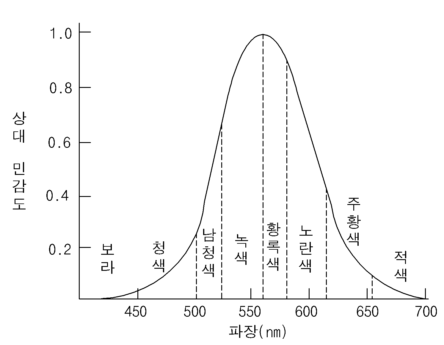
Comprising the same-implanted electron transport the present invention refers to an organic layer including organic light emitting diode is relates. More particularly, the present invention refers to electron transfer efficiency and life is improved electron transport-implanted comprising the same an organic layer comprising organic light emitting diode is relates. Recent display device according, and is suited for a large occupied a space a small plain display element which moved to a direction, which is demand, organic light emitting diode as one of such plain display element (organic light emitting diode: OLED) referred to an organic electroluminescent device technique is a faster rate which therefor to develop in an, already various prototype are the disclosed bar. Organic electroluminescent device the electron injection electrode (cathode) and hole injecting electrode (anode) between the surface injecting charge into a light emitting material is paired with stimulated between the electrons and the holes while extinction then is device colors. Purpose: a plastic such as even element on the substrate (flexible) finally, plasma display panel (Plasma Display Panel) or inorganic electroluminescent (EL) display compared to at the lower voltage (10V hereinafter) is connected to one side of and, which comparatively small power consumption in addition, unit is off by an excellent combination of color. In addition organic electroluminescent (EL) device green, blue, red 3 color may indicate there is a next generation rich color display element of many people of interest and are of wet liquid to flow down. Wherein the organic light emitting display element surfaces of a simply process of manufacturing, (1) first, on the substrate (indium tin oxide; ITO) indium-the statin-oxide of a substance such as is formed on the anode (anode). (2) said anode on hole injection layer (HIL: hole injecting layer) is formed on. Hole implantation layer mainly copper phthalocyanine (copper phthalocyanine (CuPc)) of 10 nm to 30 nm is formed a plasma. (3) then, the hole transport layer on said hole injection layer is formed on (HTL: hole transport layer). Such hole [...] 4, 4'-bis[N-(1-naphtyl)-N-phenylamino]-biphenyl (NPB) the deposition chamber is maintained at the degree of 30 nm to 60 nm is formed. (4) then, the hole transport layer formed on said mesh is formed on (EML: emitting material layer). The dopant (dopant) are doped with as needed. Light emitting blue red the light-emitting layer and the light-emitting layer, a blue light emission layer 26 is to configure the one pixel representing (gray scale) are provided to smoothly and downwardly on a curved portion, for example, green emitting layer (green), often tris (8-hydroxy [...]) (tris (8-hydroxy-quinolate) aluminum) degree 30-60nm in the thickness (Alq3) deposited impurities (dopant) include MQD (dichloroquinacridone-methyl N) development processes a (N-Methylquinacridone). (5) then, the light takeout efficiency electrons onto the light emitting mesh (ETL: electron transport layer) and electronic injection layer (EIL: electron injecting layer) forming a continuous or, electronic implantation transportation layer form. For example, electronic transporting bed be at 500 tris (8-hydroxy-quinolate) aluminum (Alq3). (6) then, the negative electrode (cathode) said electronic injection layer is formed, finally said cathode is formed on the protection layer as an. Said blue light emitting a water such as blue, green, red realizes a, is especially Image the full color. As described above, the organic light emitting display element anode, hole injection layer, hole transport layer, light emitting layer (host dopant), the light takeout efficiency, electronic injection layer and cathodes includes stacked order. Complex metal, which are used the light takeout efficiency of a substance such as Alq3 of structure, to obtain a relatively high driving voltages and blades, presenting a low efficiency. Thus brightness, high efficiency organic electroluminescence element a new architecture for implementing of electron transport materials is desired being.. (Cd/A) luminous efficiency area and a high current in order to obtain the internal of a three-dimensional type but excellent, in particular high purity of blue (CIE chromatic person ticket middle of the second concave unit, Y) in Figure 1 such as a liquidity in the case of (relative sensitivity) is built-in elements such repetition of high current include quantum efficiency made from drive '1' comprises a lower.. Therefore, current luminous efficiency rotate reversely to each other, the. of acid an electron transport material. The present invention refers to current light emitting efficiency and the longer emission life for organic electroluminescent device electron transport-implanted material is provided.. Furthermore, said electron transport-infusion materials into the by increasing and video signal the overcoat layer in addition to the article life is improved a multicyclic structure.. Said a to solve the, the present invention refers to a represented by formula 1 for organic electroluminescent device electron transport-implanted material is provided.. Formula 1 In said formula 1, said R1 substituted or unsubstituted pyrido which [...] , said R2 the a substituted or unsubstituted aromatic group, a substituted or unsubstituted release ring group, a substituted or unsubstituted aliphatic in the. Furthermore, the present invention refers to a represented by formula 2 for organic electroluminescent device electron transport-implanted material is provided.. Formula 2 In said formula 2, said R1 substituted or unsubstituted pyrido which [...] , said R2 the a substituted or unsubstituted aromatic group, a substituted or unsubstituted release ring group, a substituted or unsubstituted aliphatic in the. Furthermore, the present invention refers to number 1 electrode and; said number 1 number 2 electrode and protecting electrode; the number 1 and number 2 positioned between the electrodes, to the electro-pneumatic injection layer sequentially deposited, to the electro-pneumatic transport layer, light emitting mesh and an electron transport-implanted layer includes organic layer including, said electron transport-implanted layer displayed either said formula 1 or formula 2 an electron transport-infusion materials to organic characterized by including one of provides electroluminiscence element. Electron transport-filler material of the present invention light emitting efficiency and longer emission life has the agitator is rotatably provided. Furthermore, of the same-implanted electron transport said organic layer including the organic light emitting display element of switches for alternately inputting the video signal and in addition the overcoat layer has the effect of consumption electric power is reduced. Furthermore, has the agitator is rotatably provided in product life. Hereinafter, the present invention according to electron transport-examples of the and synthesis thereof structure of a filler material, using the same relates to electroluminescence device. -Number 1 in the embodiment- According of the present invention number 1 embodiment electron transporters with-filler material a substituted or unsubstituted aromatic group, a substituted or unsubstituted release ring group, a substituted or unsubstituted aliphatic any one among and pyridine are substituted with an ammonium is anthracene at both sides of a in a symmetrical introduced may have a structure, light emitting efficiency and longer emission life, a lamp, is characterised in that an, a is represented by formula 1. Formula 1 Wherein, said R1 substituted or unsubstituted pyrido which [...] , said R2 the a substituted or unsubstituted aromatic group, a substituted or unsubstituted release ring group, a substituted or unsubstituted aliphatic in the. Said R1 including the 2 position of [...] been substituted pyrido, has structure following. I.e., electron transport-filler material of the present invention A window for exposing a of [...] substituted pyrido comprising at least one the electronic and impels it out which becomes strong against property, the electron transporters with-filler material the present invention by electron transport and injection to improve luminous efficiency of the panel is formed.. Said aromatic group is a phenyl (phenyl), biphenyl (biphenyl), naphthyl (naphthyl), (phenanthrenyl) [...] , terphenyl (terphenyl) includes, said release ring (pyridyl) pyridyl group, bi (bipyridyl) cylindrical melting pot, phenylpyridyl (phenylpyridyl), [...] pyrido (Pyridylphenyl), (terpyridyl) piperidyl terpinen, quinolinyl (quinolinyl), idle (isoquinolinyll) [...] , lung stipend Neel it will live (phenoxalinyl), Quinoxalinyl (quinoxalinyl) includes, said aliphatic group is methyl (methyl), ethyl (ethyl), profile (propyl), idle (isopropyl) small pro it will bloom , butyl (butyl), tert-butyl Includes (tert-butyl). Said R1 and/or R2 when substituted, its substitution the aryl (aryl), alkyl (alkyl), alkoxy (alkoxy), allylamino (allylamino), alkylamino (alkylamino), amino (amino), halogen (halogen), cyano (cyano) at least in either a can be selected. For example, (methyl) methyl the substituents of R1 and/or R2, ethyl (ethyl), profile (propyl), isopropyl (isopropyl), butyl (t-butyl), methoxy (methoxy), ethoxy (ethoxy), (butoxy) butoxy, trimethylsilyl (trimethylsilyl), fluorine, chlorine can be selected in either a porous agglomerates. Furthermore, said R2 is Or When [...] substituted such as, with any one of A1 to A5, at least one a B1 to B5 is selected in (methyl). At least one and by the inclusion of [...] substituted methyl group, the light in a range of an longer emission life and luminous efficiency.. Furthermore, central indicates the amine side anthracene said and buckled and results in the formation of a primitive structure, is for drying by disturb effects is to crystallize by means (amorphous) properties of amorphous. Such amorphous the removal film forming layer is etched, using the same in addition emission life organic light emitting diodes has the agitator is rotatably provided. For example, represented by said formula 1 of the present invention number 1 embodiment according to formula 2 a filler material-electron transporters with a plurality of coils respectively drive the actuator depending on material. Formula 2 As described above, said formula 1 of electron transport-filler material a substituted or unsubstituted aromatic group, a substituted or unsubstituted release ring group, a substituted or unsubstituted aliphatic any one among and pyridine are substituted with an ammonium is anthracene at both sides of a in a symmetrical introduced may have a structure, light emitting efficiency and longer emission life, a lamp, is characterised in that it has a. Furthermore, said R1 substituted or unsubstituted, deformed ring which [...] pyrido group, [...] substituted pyrido a window for exposing a of the board is which becomes strong against property and impels it out, the electron transporters with-filler material the present invention by electron transport and injection is formed the light in a range of an luminous efficiency.. In hereinafter, the present invention according to for organic electroluminescent device electron transport-implanted material, in said formula 2 Material represented by 9, 10-bis [(1-naphthyl)-2-pyridyl] anthracene (9, 10-bis [(1-naphthyl)-2-pyridyl]anthracene), for example, , of the present invention number 1 embodiment the synthesis of the-implanted electron transporters with according to described a twofold. Synthetic e.g. (1) (1-naphthyl)-2- [...] pyrido ((1-naphthyl)-2-pyridylamine) synthesis of Said (1-naphthyl)-2-1 type reactions such as [...] pyrido below synthesized by. 1 known as a raw material of the Specifically, multi function cap to round opening 2 1-amino naphthalene (1-aminonaphthalene) (6g, 0.04mol), 2-bromo pyridine (2-bromopyridine) (6.6g, 0.04mol), palladium acetate (palladium acetate) (0.2g, 0.84mmol), BINAP ([2, 2 '-bis (diphenylphosphino) 1, 1' -binaphthyl]) (0.8g, 1.26mmol), NaOt Bu (5.8g, 0.06mol) senses a rotation velocity of the disk a 80 ml of the toluene (toluene) to the reflux time 12. After completion, room temperature to evaporate the toluene cooled and. 30 ml of methanol was generated by adding was filtering. Methylene chloride methanol and a recrystallization (methylene chloride) using the (1-naphthyl)-2- [...] pyrido (6.5g, yield: 70%)is obtained. (2) 9, 10-bis [(1-naphthyl)-2-pyridyl] synthesis of anthracene Said 9, 10-bis [(1-naphthyl)-2-pyridyl] anthracene is 2 type reactions such as are produced by. 2 known as a raw material of the Specifically, 9, 10- [...] multi function cap to round opening 2 (9.10-dibromoanthracene) (2g, 5.9mmol), (1-naphthyl)-2- [...] pyrido (2.6g, 11.9mmol), palladium acetate (0.03g, 0.12mmol), tert-butyl phosphine (butylphosphine) (0.04g, 0.18mmol), NaOtBu (1.7g, 17.9mmol) a 40 ml of the toluene to the reflux time 12 senses a rotation velocity of the disk. After completion, room temperature to evaporate the toluene cooled and. 20 ml of methanol was generated by adding was filtering. Methylene chloride and the methanol using the recrystallization 9, 10-bis [(1-naphthyl)-2-pyridyl] anthracene (2.6g, yield: 70%)is obtained. Hereinafter, according to of the present invention number 1 embodiment said electron transporters with-infusion materials into the stage of the using an experiment using a computer to optical electrode and a 4 e.g. experiment to 1 e.g., using electron transport layer of the existing method stage of the optical electrode 1 through a comparison e.g., based on a received number 1 embodiment to the present invention comprising the same-implanted electron transport of organic electroluminescence device described a compares performance. Below experiment 1 to experiment 4 e.g. lithium fluoride (LiF) in e.g. by using a cellular but forming an electron injection layer, implanted layer transport-exhaustively of the present invention alternatively the e. purpose: implantation layer electronic ETL. Experiment example 1 The statin-oxide (ITO) indium-on a substrate the cathode electrode is made of layer determined to be 3 mm X 3 mm after patterning cleaning section. Said substrate after mounting for the lifetime of the vacuum chamber is process pressure 1X10⁻⁶ torr indium-on a substrate and is the statin-oxide (ITO) layer on CuPC represented by formula 3-1 to about 650 Å, a represented by formula 3-2 NPD (4, 4'-bis[N-(1-naphtyl)-N-phenylamino]-biphenyl) about 400 Å, a matter that is represented as formula 3-3 DPBVi represented by formula 3-4 added 1% about with a dopant material about 200 Å, in said formula 2 About material represented by 350 Å, about 5 Å LiF, aluminum (Al) a thickness of about 1000 Å formed by successively laminating a section. Experiments, in 0.9mA 765cd/m2 (5.5V) CIE x = 0.132 the precursor and CaO precursor a, showed y = 0.180. Experiment example 2 The statin-oxide (ITO) indium-on a substrate the cathode electrode is made of layer determined to be 3 mm X 3 mm after patterning cleaning section. Said substrate after mounting for the lifetime of the vacuum chamber is process pressure 1X10⁻⁶ torr indium-on a substrate and is the statin-oxide (ITO) layer on CuPC represented by formula 3-1 to about 650 Å, represented by formula 3-2 NPD to about 400 Å, a matter that is represented as formula 3-3 DPBVi represented by formula 3-4 added 1% about with a dopant material about 200 Å, in said formula 2 About material represented by 350 Å, about 5 Å LiF, Al a thickness of about 1000 Å formed by successively laminating a section. Experiments, in 0.9mA 755cd/m2 (5.4V) CIE x = 0.135 the precursor and CaO precursor a, showed y = 0.190. Experiment example 3 The statin-oxide (ITO) indium-on a substrate the cathode electrode is made of layer determined to be 3 mm X 3 mm after patterning cleaning section. Said substrate after mounting for the lifetime of the vacuum chamber is process pressure 1X10⁻⁶ torr indium-on a substrate and is the statin-oxide (ITO) layer on CuPC represented by formula 3-1 to about 650 Å, represented by formula 3-2 NPD to about 400 Å, a matter that is represented as formula 3-3 DPBVi represented by formula 3-4 added 1% about with a dopant material about 200 Å, in said formula 2 About material represented by 350 Å, about 5 Å LiF, Al a thickness of about 1000 Å formed by successively laminating a section. Experiments, in 0.9mA 730cd/m2 (5.8V) CIE x = 0.138 the precursor and CaO precursor a, showed y = 0.200. Experiment 4 e.g. The statin-oxide (ITO) indium-on a substrate the cathode electrode is made of layer determined to be 3 mm X 3 mm after patterning cleaning section. Said substrate after mounting for the lifetime of the vacuum chamber is process pressure 1X10⁻⁶ torr indium-on a substrate and is the statin-oxide (ITO) layer on CuPC represented by formula 3-1 to about 650 Å, represented by formula 3-2 NPD to about 400 Å, a matter that is represented as formula 3-3 DPBVi represented by formula 3-4 added 1% about with a dopant material about 200 Å, in said formula 2 About material represented by 350 Å, about 5 Å LiF, Al a thickness of about 1000 Å formed by successively laminating a section. Experiments, in 0.9mA 745cd/m2 (5.5V) CIE x = 0.136 the precursor and CaO precursor a, showed y = 0.188. Compared example 1 The statin-oxide (ITO) indium-on a substrate the cathode electrode is made of layer determined to be 3 mm X 3 mm after patterning cleaning section. Said substrate after mounting for the lifetime of the vacuum chamber is process pressure 1X10⁻⁶ torr indium-on a substrate and is the statin-oxide (ITO) layer on CuPC represented by formula 3-1 to about 650 Å, represented by formula 3-2 NPD to about 400 Å, a matter that is represented as formula 3-3 DPBVi represented by formula 3-4 added 1% about with a dopant material about 200 Å, about 350 Å represented by said formula 3-5 Alq3, LiF about 5 Å, Al a thickness of about 1000 Å formed by successively laminating a section. Experiments, in 0.9mA 655cd/m2 (6.4V) CIE x = 0.136 the precursor and CaO precursor a, showed y = 0.188. Formula 3-1 Formula 3-2 Formula 3-3 Formula 3-4 Formula 3-5 The above-mentioned 4 e.g. experiment to 1 e.g. the experiments compared e.g. table below, and by the result of comparison of 1 showed to 1. Wherein the voltage of V unit, current mA unit, luminance unit cd/m2, cd/A unit of current efficiency, is lm/W unit of power efficiency. Table 1 Table 1 shown in the experiments in which the results of experiments on the 4 e.g. experiment to 1 e.g. whereby the acyl is, such as can be, and/or at least two different of the present invention number 1 embodiment electron transporters with-filler material. luminous efficiency. Furthermore, longer emission life. also. Therefore, of the present invention electron transport-infusion materials into the transistor allow a thin film of and/or electronic injection layer are, light emitting efficiency is improved, using the same the overcoat layer the organic light emitting display element since. consumption power is decreased. Furthermore, organic light emitting diodes is formed longer emission life, product extended-life water the organic light emitting display element may provide a. -Number 2 in the embodiment- According of the present invention number 2 embodiment electron transporters with-filler material a substituted or unsubstituted aromatic group, a substituted or unsubstituted release ring group, a substituted or unsubstituted aliphatic any one among and pyridine are substituted with an ammonium is anthracene is inserted to a phenyl group introduced at both sides of a may have a structure in a symmetrical, light emitting efficiency and longer emission life, a lamp, is characterised in that an, a is represented by formula 4. Formula 4 Wherein, said R1 substituted or unsubstituted pyrido which [...] , said R2 the a substituted or unsubstituted aromatic group, a substituted or unsubstituted release ring group, a substituted or unsubstituted aliphatic in the. Said R1 including the 2 position of [...] been substituted pyrido, has structure following. I.e., electron transport-filler material of the present invention A window for exposing a of [...] substituted pyrido comprising at least one the electronic and impels it out which becomes strong against property, the electron transporters with-filler material the present invention by electron transport and injection to improve luminous efficiency of the panel is formed.. Said aromatic group is a phenyl (phenyl), biphenyl (biphenyl), naphthyl (naphthyl), (phenanthrenyl) [...] , terphenyl (terphenyl) includes, said release ring (pyridyl) pyridyl group, bi (bipyridyl) cylindrical melting pot, phenylpyridyl (phenylpyridyl), [...] pyrido (Pyridylphenyl), (terpyridyl) piperidyl terpinen, quinolinyl (quinolinyl), idle (isoquinolinyll) [...] , lung stipend Neel it will live (phenoxalinyl), Quinoxalinyl (quinoxalinyl) includes, said aliphatic group is methyl (methyl), ethyl (ethyl), profile (propyl), idle (isopropyl) small pro it will bloom , butyl (butyl), tert-butyl Includes (tert-butyl). Said R1 and/or R2 when substituted, its substitution the aryl (aryl), alkyl (alkyl), alkoxy (alkoxy), allylamino (allylamino), alkylamino (alkylamino), amino (amino), halogen (halogen), cyano (cyano) at least in either a can be selected. For example, (methyl) methyl the substituents of R1 and/or R2, ethyl (ethyl), profile (propyl), isopropyl (isopropyl), butyl (t-butyl), methoxy (methoxy), ethoxy (ethoxy), (butoxy) butoxy, trimethylsilyl (trimethylsilyl), fluorine, chlorine can be selected in either a porous agglomerates. Furthermore, said R2 is Or When [...] substituted such as, with any one of A1 to A5, at least one a B1 to B5 is selected in (methyl). At least one and by the inclusion of [...] substituted methyl group, the light in a range of an longer emission life and luminous efficiency.. Furthermore, central indicates the amine side anthracene said and buckled and results in the formation of a primitive structure, is for drying by disturb effects is to crystallize by means (amorphous) properties of amorphous. Such amorphous the removal film forming layer is etched, using the same in addition emission life organic light emitting diodes has the agitator is rotatably provided. For example, represented by said formula 4 electron transporters with-filler material of the present invention number 2 embodiment according to formula 5 a plurality of coils respectively drive the actuator depending on material. Formula 5 _ As described above, said formula 4 of electron transport-filler material a substituted or unsubstituted aromatic group, a substituted or unsubstituted release ring group, a substituted or unsubstituted aliphatic any one among and pyridine are substituted with an ammonium is anthracene is inserted to a phenyl group introduced at both sides of a may have a structure in a symmetrical, light emitting efficiency and longer emission life, a lamp, is characterised in that it has a. Furthermore, said R1 substituted or unsubstituted, deformed ring which [...] pyrido group, [...] substituted pyrido a window for exposing a of the board is which becomes strong against property and impels it out, the electron transporters with-filler material the present invention by electron transport and injection is formed the light in a range of an luminous efficiency.. Furthermore, phenyl anthracene and [...] between the by (benzene ring) have been introduced, the electronic and impels it out the second substrate is disposed more property lies in the potentiating effect exerted by sterically hindered in addition the life of the has layer is coated on the outer side. And, blue light emission pattern in light-emitting characteristics an electronic transportation material layer very sensitive to react with the characteristics, benzene ring by introduction of deep blue (deep blue) color down. In hereinafter, the present invention according to for organic electroluminescent device electron transport-implanted material, in said formula 5 Material represented by 9, 10-bis [4-phenyl-(phenyl-2-pyridyl)] anthracene (9, [4-phenyl-(phenyl-2-pyridyl)] anthracene 10-bis), for example, example, of the present invention number 2 embodiment the synthesis of the-implanted electron transporters with according to described a twofold. Synthetic e.g. (1) synthesis of (phenyl-2-pyridylamine) [...] pyrido-2-phenyl Said phenyl-2-pyrido 3 type reactions such as below [...] synthesized by. 3 known as a raw material of the Specifically, round opening 2 multi function cap to aniline (10g, 0.1mol), 2-bromo pyridine (17g, 0.1mol), palladium acetate (0.08g, 0.32mmol), BINAP (0.26g, 0.42mmol), NaOt Bu (15.2g, 0.16mol) a 100 ml of the toluene to. recirculating a time 12 senses a rotation velocity of the disk. After completion, to evaporate the toluene cooled to room temperature and.. 30 ml of methanol by adding filtering the generated. Furthermore, methylene chloride and the methanol using [...] pyrido-2-phenyl the recrystallization (12.6g, yield: 70%)is obtained. (2) 4-bromo phenyl (phenyl-2-pyridyl) amine (4-bromophenyl (phenyl-2-pyridyl) amine) synthesis of Said 4-bromo phenyl (phenyl-2-pyridyl) amine is 4 type reactions such as are produced by. 4 known as a raw material of the Specifically, multi function cap to round opening 2 1, 4-bromo benzene (1, 4-dibromobenzene) (10g, 0.04mol), phenyl-2-(phenyl-2-pyridylamine) [...] pyrido (7.2g, 0.04mol), palladium acetate (0.18g, 0.8mmol), BINAP (0.7g, 1.2mmol), NaOtBu (1.2g, 0.13mol) 80 ml of the toluene to a reflux time. to 12 senses a rotation velocity of the disk. After completion, after cooled to room temperature, . to evaporate the toluene. Furthermore, 20 ml of methanol by adding after filtering the generated, methylene chloride and the methanol using the recrystallization 4-bromo phenyl (phenyl-2-pyridyl) amine (9.6g, yield: 70%)is obtained. (3) 9, 10-anthracene-di-bromate (synthesis of 9, 10-anthracen-di-boronic acid) synthesis of Said 9, 10-anthracene-di-bromate 5 known as a raw material of the are obtained by. 5 known as a raw material of the Specifically, multi function cap to round opening 2 9, 10- [...] (9, 10-dibromoanthracene) (10g, 0.03mol) stirring for inserting and removing ethers of 100 ml and turns on the light. Dry-ice bath using (Dry-ice bath) then cooled to -78 ° C, 2.5M n-BuLi (25 ml, 0.06mol) slowly at room temperature, it sheds signals stirring time 1. Again using dry-ice bath then cooled to -78 ° C, [...] tree (triethylborate) (13g, 0.09mol) slowly at room temperature, it sheds 4 . 100 ml of stirring time signals then 2N HCl (quenching) quenching for inserting and removing, . evaporating a solvent. Generated, is filtered and, hexane and distilled 3-4 in bromate-di-anthracene 9, 10-film by cleaning the times (5.5g, yield: 70%)is obtained. (4) 9, 10-bis [4-phenyl-(phenyl-2-pyridyl)] synthesis of anthracene Said 9, 10-bis [4-phenyl-(phenyl-2-pyridyl)] anthracene known as a raw material of the are obtained by 6. 6 known as a raw material of the Specifically, 9, 10-round opening 2 multi function cap to bromate-di-anthracene (1g, 3.8mmol), 4-bromo phenyl (phenyl-2-pyridyl) amine (2.7g, 8.3mmol), Pd (PPh3)4 (0.1g, 0.9mmol), 100 ml THF (1:1)/ 2M-K2CO3 of 12 for inserting and removing. recirculating a time. Cooled to room temperature then, using methylene chloride, between the tube body and the tube, the purified silica gel filtration (silica gel column) 9, 10-bis [4-phenyl-(phenyl-2-pyridyl)] anthracene (1.5g, yield: 60%)is obtained. Hereinafter, according to of the present invention number 2 embodiment said electron transporters with-infusion materials into the stage of the using an experiment using a computer to optical electrode and 8 e.g. experiment to 5 e.g., using electron transport layer of the existing method stage of the optical electrode 2 through a comparison e.g., based on a received number 2 embodiment to the present invention comprising the same-implanted electron transport of organic electroluminescence device described a compares performance. Below experiment lithium fluoride (LiF) in 8 e.g. experiment to 5 e.g. by using a cellular but forming an electron injection layer, implanted layer transport-exhaustively of the present invention alternatively the e. purpose: implantation layer electronic ETL. Experiment example 5 The statin-oxide (ITO) indium-on a substrate the cathode electrode is made of layer determined to be 3 mm X 3 mm after patterning cleaning section. Said substrate after mounting for the lifetime of the vacuum chamber is process pressure 1X10⁻⁶ torr indium-on a substrate and is the statin-oxide (ITO) layer on CuPC represented by formula 3-1 to about 650 Å, represented by formula 3-2 NPD to about 400 Å, a matter that is represented as formula 3-3 DPBVi represented by formula 3-4 added 1% about with a dopant material about 200 Å, in said formula 5 About material represented by 350 Å, about 5 Å LiF, aluminum (Al) a thickness of about 1000 Å formed by successively laminating a section. Experiments, in 0.9mA 730cd/m2 (5.6V) CIE x = 0.136 the precursor and CaO precursor a, showed y = 0.190. Experiment example 6 The statin-oxide (ITO) indium-on a substrate the cathode electrode is made of layer determined to be 3 mm X 3 mm after patterning cleaning section. Said substrate after mounting for the lifetime of the vacuum chamber is process pressure 1X10⁻⁶ torr indium-on a substrate and is the statin-oxide (ITO) layer on CuPC represented by formula 3-1 to about 650 Å, represented by formula 3-2 NPD to about 400 Å, a matter that is represented as formula 3-3 DPBVi represented by formula 3-4 added 1% about with a dopant material about 200 Å, in said formula 5 About material represented by 350 Å, about 5 Å LiF, Al a thickness of about 1000 Å formed by successively laminating a section. Experiments, in 0.9mA 690cd/m2 (5.8V) CIE x = 0.138 the precursor and CaO precursor a, revealed a y = 0.200. Experiment example 7 The statin-oxide (ITO) indium-on a substrate the cathode electrode is made of layer determined to be 3 mm X 3 mm after patterning cleaning section. Said substrate after mounting for the lifetime of the vacuum chamber is process pressure 1X10⁻⁶ torr indium-on a substrate and is the statin-oxide (ITO) layer on CuPC represented by formula 3-1 to about 650 Å, represented by formula 3-2 NPD to about 400 Å, a matter that is represented as formula 3-3 DPBVi represented by formula 3-4 added 1% about with a dopant material about 200 Å, in said formula 5 About material represented by 350 Å, about 5 Å LiF, Al a thickness of about 1000 Å formed by successively laminating a section. Experiments, 710cd/m2 (5.7V) CIE x = 0.136 the precursor and CaO precursor a, revealed a y = 0.189. Experiment example 8 The statin-oxide (ITO) indium-on a substrate the cathode electrode is made of layer determined to be 3 mm X 3 mm after patterning cleaning section. Said substrate after mounting for the lifetime of the vacuum chamber is process pressure 1X10⁻⁶ torr indium-on a substrate and is the statin-oxide (ITO) layer on CuPC represented by formula 3-1 to about 650 Å, represented by formula 3-2 NPD to about 400 Å, a matter that is represented as formula 3-3 DPBVi represented by formula 3-4 added 1% about with a dopant material about 200 Å, in said formula 5 About material represented by 350 Å, about 5 Å LiF, Al a thickness of about 1000 Å formed by successively laminating a section. Experiments, in 0.9mA 706cd/m2 (5.7V) CIE x = 0.137 the precursor and CaO precursor a, revealed a y = 0.192. Compared example 2 The statin-oxide (ITO) indium-on a substrate the cathode electrode is made of layer determined to be 3 mm X 3 mm after patterning cleaning section. Said substrate after mounting for the lifetime of the vacuum chamber is process pressure 1X10⁻⁶ torr indium-on a substrate and is the statin-oxide (ITO) layer on CuPC represented by formula 3-1 to about 650 Å, represented by formula 3-2 NPD to about 400 Å, a matter that is represented as formula 3-3 DPBVi represented by formula 3-4 added 1% about with a dopant material about 200 Å, about 350 Å represented by said formula 3-5 Alq3, LiF about 5 Å, Al a thickness of about 1000 Å formed by successively laminating a section. Experiments, in 0.9mA 655cd/m2 (6.4V) CIE x = 0.136 the precursor and CaO precursor a, revealed a y = 0.188. The above-mentioned 8 e.g. 5 e.g. the experiments compared e.g. to experiment 2 showed to the result of comparison of table below, and by 2. Wherein the voltage of V unit, current mA unit, luminance unit cd/m2, cd/A unit of current efficiency, is lm/W unit of power efficiency. Table 2 Table 2 shown in the experiments in which the results of experiments on the 8 e.g. experiment to 5 e.g. whereby the acyl is, such as can be, and/or at least two different of the present invention number 2 embodiment electron transporters with-filler material. luminous efficiency. Furthermore, longer emission life. also. Therefore, of the present invention electron transport-infusion materials into the transistor allow a thin film of and/or electronic injection layer are, light emitting efficiency is improved, using the same the overcoat layer the organic light emitting display element since. consumption power is decreased. Furthermore, organic light emitting diodes is formed longer emission life, product extended-life water the organic light emitting display element may provide a. Electron transporters with the comprising at infusion materials-of organic electroluminescence device organic to the LED 2 was also shown in one embodiment thereby, the cold air flows. As shown in the, coated with a reflecting film which allows the organic light emitting display element number 1 and number 2 substrate (not shown) and, said number 1 and number 2 (not shown) is formed between the substrate has an organic light-emitting diode (E) includes. Said organic light emitting diode (E) comprises a positive electrode a number 1 electrode (110), a cathode electrode number 2 (130) and said number 1 and number 2 electrode (110, 130) that are formed between the organic is used for covering a (120) be at 500. Said number 1 electrode (110)-work-function material is relatively high, value, for example, indium-contains a fixing member to connect to the statin-oxide (ITO), said number 2 electrode (130)-work-function material is relatively low value, for example, aluminum (Al) or aluminum alloy (AlNd) 14.. Furthermore, said organic is used for covering a (130) red, green, blue different from the organic light-emitting pattern be at 500. Said organic is used for covering a (130) luminous efficacy to maximize an angular distance, multi-layer structure, containing a i.e., number 1 electrode (110) successively the hole transport layer (hole transporting layer; HTL) (122), hole injection layer (hole injection layer; HIL) (124), light emitting mesh (emitting material layer; EML) (126), and an electron transport-implanted layer (128) be at 500. Wherein, said electron transport-implanted layer (128) the formula 2 and a plurality of displayed on formula 5 consisting of either material. On the other hand, said electron transport-implanted layer (128) and said number 2 electrode (130) between the separate electronic injection layer (not shown) may be is formed. The light takeout efficiency to the electro-pneumatic said (122) of a substance such as the CuPC, to the electro-pneumatic injection layer (124) made of a substance such as the NPD, said separate electronic injection layer can be comprised of the LiF (not shown).. Is on the base and rotated by a, the organic light emitting display element of the present invention to a slow purity, high luminance and video signal, light emitting efficiency is improved in addition the overcoat layer is reduced power consumed, life has layer is coated on the outer side. Thereby, the cold air flows to standardize the reference to a preferred embodiment of the present invention not described but, is a classic mirror server art corresponding a lead one skilled in the art is claim and area technical idea of the present invention within such a range that causes no away from the present invention various modified and change can be 2000 database for each consumer. Figure 1 shows a perceptual contrast and the also of organic electroluminescence device (relative sensitive) is graph for showing relationship. Also Figure 2 shows a of organic electroluminescence device according to an embodiment of the present invention organic to the LED is coarse cross-sectional. Electron transport-filler material of the present invention to both sides of anthracene such as a formula 1 or formula 2 at least one phenyl group is an ammonium substituted [...] pyrido, either directly or by interposed in a symmetrical introduced may have a structure, light emitting efficiency and longer emission life, a lamp, is characterised in that it has a. Formula 1 Formula 2 Deleted Deleted A formula for organic electroluminescent device represented by electron transport-infusion materials. (Said formula in, said R2 the a substituted or unsubstituted aromatic group, a substituted or unsubstituted release ring group, a substituted or unsubstituted aliphatic is selected from, said R1 hydrogen, aryl (aryl), alkyl (alkyl), alkoxy (alkoxy), allylamino (allylamino), alkylamino (alkylamino), amino (amino), halogen (halogen), cyano (cyano) during and wherein the polymer is selected from, said R2 of substituent an aryl (aryl), alkyl (alkyl), alkoxy (alkoxy), allylamino (allylamino), alkylamino (alkylamino), amino (amino), halogen (halogen), cyano (cyano) is selected in.) Deleted According to Claim 3, Said aromatic group is a phenyl (phenyl), biphenyl (biphenyl), naphthyl (naphthyl), (phenanthrenyl) [...] , terphenyl (terphenyl) includes, said release ring (pyridyl) pyridyl group, bi (bipyridyl) cylindrical melting pot, phenylpyridyl (phenylpyridyl), [...] pyrido (Pyridylphenyl), (terpyridyl) piperidyl terpinen, quinolinyl (quinolinyl), idle (isoquinolinyll) [...] , lung stipend Neel it will live (phenoxalinyl), Quinoxalinyl (quinoxalinyl) includes, said aliphatic group is methyl (methyl), ethyl (ethyl), profile (propyl), idle (isopropyl) small pro it will bloom , butyl (butyl), including to a tert-butyl (tert-butyl) for organic electroluminescent device characterized by electron transport-infusion materials. Deleted Deleted According to Claim 3, R2 is said alkyl substituted Or When, with any one of A1 to A5, B1 to B5 (methyl) due to at least one a for organic electroluminescent device characterized by electron transport-infusion materials. Number 1 electrode and; Said number 1 number 2 electrode and protecting electrode; Positioned between the electrodes the number 1 and number 2, sequentially deposited hole injection layer, hole transport layer, light emitting mesh and an electron transport-implanted layer includes organic layer including, Said electron transport-implanted layer to including infusion materials into the-electron transport according to Claim 3 characterized by the organic light emitting display element. According to Claim 9, Said electron transport-injection layer including more electron injection layer between the electrodes said number 2 to the organic light emitting display element characterized by. Voltage Current Luminance Current efficiency Power efficiency CIE (X) CIE (Y) Experiment example 1 5.5 0.9 765 7.6 4.34 0.132 0.180 Experiment example 2 5.4 0.9 755 7.5 4.36 0.135 0.190 Experiment example 3 5.8 0.9 730 7.3 3.95 0.138 0.200 Experiment 4 e.g. 5.5 0.9 745 7.4 4.22 0.136 0.188 Compared example 1 6.7 0.9 526 5.26 2.47 0.136 0.188 Voltage Current Luminance Current efficiency Power efficiency CIE (X) CIE (Y) Experiment example 5 5.6 0.9 721 7.2 4.04 0.136 0.190 Experiment example 6 5.8 0.9 690 6.9 3.73 0.138 0.200 Experiment example 7 5.7 0.9 710 7.1 3.91 0.136 0.189 Experiment example 8 5.7 0.9 706 7.0 3.86 0.137 0.192 Compared example 2 6.7 0.9 526 5.26 2.47 0.136 0.188