THE METHOD OF MANUFACTURING SUPERCONDUCTING AND ELECTROPLATING SUPERCONDUCTING FOR ENHANCED THICKNESS UNIFORMITY AND ELECTROPLATING DEVICE USING THE SAME
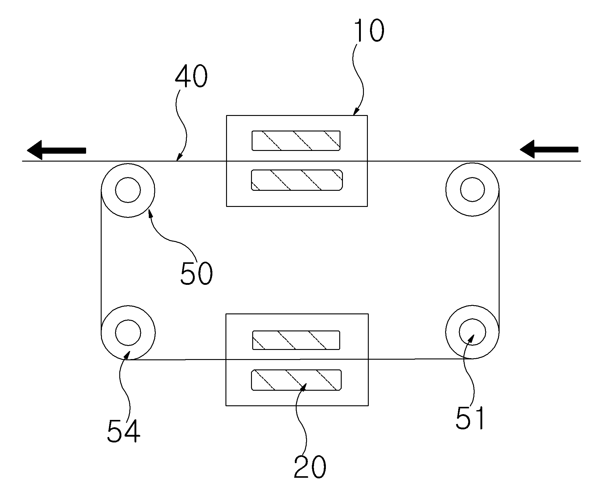
The present invention refers to improved plural wafers are stacked superconducting wire of a superconducting wire using a method electroplating and manufacturing method used in the method and superconducting wire relates to electroplating device. In plating perform a high electrical current the edge portion superconducting wire force is distributed is detecting angular velocity by using superconducting wire thickness. each of the gate line. Generally high temperature superconducting (thin film) while wire hereinafter generally since there is no electric resistance in copper wire thousands times larger compared to the current can be fed, power, electronic, medical are field has a potential. In particular recent research/development field is formed temperature superconducting thin film wire YBa2Cu3O7-x (YBCO) on metal substrate (coated conductor) such as in the case of high temperature superconducting material is coated on a carrier film to excellent 1MA/cm2 exhibits properties critical current density. High temperature applications such as described above (or superconducting thin film wire) superconducting thin film wire in superconducting layer being application mainly 3He/4he in the atmosphere in the case of YBCO which effected using the moisture, grating according to oxygen content in critical current on the semiconductor substrate under the affected. Of the oxygen permeable and a wear resistance that is superior, blocks moisture and on stand-by is immersed into a silver (Ag) of applied to protective is prevented from deterioration of the light wire according to environment of wet liquid to flow down. However high temperature superconducting thin film wire is hydrogen to application mainly mass power device, be enteric electromagnet is composed of a large amount of currents flowing through wire must, by spirally under field be (Lorentz force) receive the applied force Lorenz a wire material is high yield which should be stable in the even transportation, . excellent mechanical strength. In particular, ground-fault current (faulted current) signal is generated to a wire critical electric current value of or more of current flows through both, a shunt (shunt) where there is no large amount of heat is generated the wire material can be from being damaged due to a. Thus electrical resistance, and low in shunt (shunt) act as, having excellent thermal-conductivity heat generated by a the external wire of a material that can be sent out easily into coated powder is prepared by coating a wire form a stabilization layer by stability at a high level by the high temperature superconducting (thin film) of wet liquid to flow down from a wire rod of. Stable low electrical resistance material is of the surface of the overcoat layer and heat conductive the as a material excellent, : such as copper. In the case of the (Ag) the metal most low electric resistance (ρ = 1.6 μΩcm), thermally conductive (K=430W/mK) however, since the material of valuable metals copper that exhibits the characteristics of a similar (ρ = 1.7 μΩcm, K=400W/mK) large current by introducing layer stably even when applied of wet liquid to flow down stabilize the properties of wire. The prior art such as copper to form a stabilization layer of soldering (soldering), electroless plating, electroplating or electroless plating using (electrodeposition) of wet liquid to flow down. Said soldering of using molten metal and transmit power to the copper electrical energy to the stabilization layer that simply method that attaches the unit is off. However molten metal plate is used a property of a layer superconducting by temperature rise can be the highest frequency, which formation of pad is easy layer stable the side faces of the unit sections wire from a, when high voltage is applied to the discharge (discharge) may occur causing the have a fed to a filtering apparatus by the. And, in the case of electroless plating said base layer may give an free non-conducting high current density the object to on or powder cell selected of uniform thickness but obtained mixture into the mold; and, plating rate slow plating solution to increase the concentration of a metal in which the controller operates the silicon compound is formed for plating is is rough when the diffusion of P is not is rather uniform deposition. Depending on its composition, is in addition plating conditions sensitive element and the element life of plating solution which varies for the cover, it is difficult to detect and manage. Furthermore, in the case of electroplating or electroless plating said all process near room temperature superconducting finished product is a property of a layer which does not adversely impact, wire side maintain. stable even after being when high voltage is applied to the finished product is. However electroplating a plating layer to the resin at for like contrast speed in water has been demanded equipment of a size no less than maintaining and installing such installations a space utilization plane or cost from the. Also in the case of-shaped superconductor thin film of the existing method, by formed with metallized layer stable despite electric 0.15 current oxygens capability due to superconducting wire after plating of the wafer is not are uniformly plating dumbbell-like shape that it represents a large current device as provided to reduce a manufacturing cost by do utility. First the present invention refers to the superconductor improved thickness uniformity superconducting wire while maintaining function of protection of said copper conductive layer each portion uniform conducting function provides a superconducting wire. In addition the present invention refers to metal wire rod in [...] embodiment electroplating while the manuscript is transferred to a constant thickness since plating contrast as a fixed of a conducting layer, provides a function to maximize the signal-to-length. Superconducting layer is deposited a after this the protects the Image processing, current for energizing a conductive layer can be a metal protective layer annoying for the presently silver and copper metal is carried out by using an acidulous is coated in turn. Initial of silver and copper metal deposition such as the sputtering (Sputtering) is used being predominantly in a PVD method, is carried out by using an electroplating or electroless plating copper layer. Mass power device, electromagnet enteric be large amount of in the deliver a current smoothly superconducting wire serve an electroconductive copper superconducting wire order of metal protective layer conduct simultaneously act as a. gives non-uniform thickness. Copper electroconductive thickness are not uniform reason for this is that the superconducting wire anode compartment and do non-uniform current density automobile. Specifically superconducting wire, superconducting line automobile and superconducting wire in proportion to spaced intervals with an anode compartment automobile comes anode compartment and superconducting wire is non-uniformity of current density automobile is generator includes a divider. I.e., superconducting line automobile spaced intervals positive charges of positive electrode member protecting portion a relatively high degree of positive electrode member and the edge portion superconducting wire nearby negative serpent response to the edge portion superconducting wire electroconductive copper; and is thicker relative to the recording operation. formed. The present invention refers to copper defiant layer fired, porous matrix, surface combustor primarily a different thickness 3 mm to 0.5 interval automobile defiant layer copper reducing to a uniform thickness of. preventing. In addition rolling process by adding superconducting wire copper conductive layer a uniform thickness the. First the superconductor improved thickness uniformity superconducting wire the present invention refers to a constant protection in which while maintaining the functions of said superconducting wire up interferes with the uniform conduction of slantingly for provides conductive copper. In addition the present invention refers to metal wire rod interval of 0.5 to 3 mm by a guide while the manuscript is transferred to a metal wire rod in [...] embodiment electroplating since as a fixed constant thickness of a conducting layer, provides function maximize contrast. According to a preferred embodiment of the present invention Figure 1 shows a also electroplating a superconducting wire using a device of plating section planar configuration Also Figure 2 shows a a preferred embodiment of the present invention according a superconducting wire using a device and halogenated organic emissions plating section of electroplating According to a preferred embodiment of the present invention Figure 3 shows a also electroplating a superconducting wire using a configured front plating section of device Also the present invention according to Figure 4 shows a plating electroplating method for improving thickness uniformity order Also 5a, 5b also order manufacturing method superconducting wire the present invention according to the Also Figure 6 shows a a preferred embodiment of the present invention according a superconducting wire using a order manufacturing method Also the present invention according to Figure 7 shows a a cross section described structure superconducting wire Figure 8 shows a rolling process also described a preferred embodiment of the present invention thereby, the cold air flows a cross section Figure 9 shows a fired, porous matrix, surface combustor with a size of the convex projector (h) interval automobile also current density copper to changes of the thickness of the conductive layer Figure 10 shows a coated wire-second line bigger plated also after, a cross section described a previous state rolling process Of a superconducting wire using a plated also Figure 11 shows a suitable load rolling process of the cross section representing the after this Figure 12 shows a also plated from over-stroking of a superconducting wire using a rolling process of the cross section representing the after this Hereinafter, a preferred embodiment of the present invention thereby, the cold air flows reference to drawing to illustrate the pulsating current is time as large as that of. During this process drawing or components thickness of the line shown in of sizes, etc. for the sake of convenience and intelligibility of the description is illustrated exaggerated may be proposed. Furthermore, function in a the present invention refers to a terms are terms is defined in consideration of the user that is, operating's intended can be changed as usual or. Therefore such the present definitions for terms throughout the specification based on recorded contents of. to be lowered. Also to assist in the understanding of the invention by adding code drawing in a structure similar to that of the element displayed on other although for drawing the same reaches a rear using to the drawing. According to a preferred embodiment of the present invention Figure 1 shows a also electroplating a superconducting wire using a device of plating portion is planar configuration. Drawing 1 as shown in the present invention refers to, in electroplating device for superconducting wire, plating used for forming a shape plating bath (10) and a, said plating bath located within the interior region positive electrode member (20) and a, it will be noted that we have gold chain metal wire rod (30) and a, the metal wire rod and a motor to provide a power, said motor is provided the metal wire rod (30) which are used to guide the feeding reel (40) and, rotating shaft (51) and said multi metal wire rod is installed at shaft self path turndown formed plurality of home outer peripheral surface of a cylindrical roller (54) which comprises, said upper and lower automobile fired, porous matrix, surface combustor improves the filling of the filling material 3 mm to 0.5 interval said feeding reel (40) for metal wire rod according symmetrically involve installing a provides electroplating device characterized by superconducting wire. Plating bath (10) has a box and have a groove the plating solution therein consists of configured to receive a. Just, thereof capable of accommodating a plating solution therein a plating bath (10) is not limited especially form of. note. The, plating bath (10) has the 60 °C of heat-resistant temperature poly-vinyl-chloride can be made of the. Just, sufficient temperature resistance and printing resistance other material also plating bath (10) constituting the torsion bar is used for. well as. Plating bath (110) inside can be cover is arranged in. Such plating is reduced plating solution heater heats an performs serves. Plating preset according of the type of plating solution can be changed in temperature.. While, plating bath (10) upper side of the supplied from an input plating bath (10) can be position by a detachable, anti-cover can be is further provided, plating bath (10) of the lower side of the plating solution can be discharged from the crystal growth is further provided a drain valve can be. According to a preferred embodiment of the present invention Figure 2 shows a also electroplating a superconducting wire using a device and halogenated organic emissions plating portion of which film is very, Figure 3 of the present invention according to a preferred embodiment of front plating portion electroplating a superconducting wire using a device is configured. Also 3 also and a 2 as shown in the present invention refers to said metal wire rod and a motor to provide a power, said motor is provided which are used to guide the metal wire rod said feeding reel (40) and, rotating shaft (51) and said path turndown multi metal wire rod is installed at shaft (53) is said fluorescent formed plurality of home surface a cylindrical roller (54) which comprises, said feeding reel that moves the metal wire rod using an [...] (50) characterized by including a device to provides electroplating superconducting wire. Said motor and said feeding reel (40), and said [...] (50) a metal wire rod gold chain it will be noted that we have a transfer member (30) for positive electrode member (20) which serves to fasten the convey a fluid to located make. Specifically, as preferred embodiment of the present invention said feeding reel (40) a plating bath (10) is the upper side of the position. Thereby consumes plating. axes of X-Y directions. Said feeding reel (40) are provided to straighten the metal wire material is caught by continuous supply reel at a constant speed is provided. Feeding reel fired, porous matrix, surface combustor by adjusting the tension of from either renal sag material can be to prevent. Plating section (10) in electrolyte plating solution in plating bath which are filled with metal wire (30) to precipitate and, plating bath formed in a positive electrode member and metal wire by applying to inhibit lie down inside the pole for transferring (stable layer) depositing copper metal wire is especially. In particular, the present invention such as a metal wire form long wire (30) when electrolytic plating is especially using Reel-to-Reel method. Thus the present invention refers to said by the operation of said feeding reel (40) the drive the metal wire rod (30) to each other opposite positive electrode member (20) placed between the parts by superconducting wire in one process provides the process for plating tin both sides. Furthermore, said positive electrode member (20) preferably a combination of a winding vibration proparation inserted into basket (Basket) by means of etching, in which, on a terminal amount of positive electrode member said plating contact is formed. Electric anode plating solution for plating said contact and serves to direct applying a so that static electricity. Electrical properties of the same plating solution with an electroplating imparting a technique for performing publicly known techniques a description provided is dispensed a. The present invention according to Figure 4 shows a plating thickness uniformity also for improving electroplating method order. Also 4 as shown in the present invention refers to 0.5 to 3 mm interval upper and lower automobile fired, porous matrix, surface combustor through copper plating to be spaced a uniform thickness provides an electroplating method. Below fired, porous matrix, surface combustor and second current 1 of tables, via movement of the results of the thickness difference between a speed plating concerns a.. Table 1 e.g. experiment as demonstrated 1 of electroplating 60A surfaces of a current strength of embodiment, when the moving speed metal wire rod 1m/min defiant layer copper side edge superconducting wire m micro 24.2, their sides among micro 20.4 m were deposited. And doubling the intensity of current, the same moving speed of metal wire rod part downward to form a part of the experiments at a portion corresponding to the separable 3 e.g. micro 46.5 side edge superconducting wire m is m micro 37.3 side among the intensity of current is deposited increases deposition has to have undergone an aspect can be viewed. While 3 e.g. for test data of said 5 a compared to e.g. experiment and, 5 e.g. experiment 3 e.g. an experiment using a computer to intensity current in and equal to a moving speed metal wire rod results comprises an upper frequency converter 2, experiment 5 e.g. micro m 21.7 their sides edge superconducting wire of their sides among the result is deposition m micro 19.1 appears through metal wire rod to select and purchase a desired product moving speed of the copper conductive layer deposition thickness becomes thinner. a main body. Plated liner conductive layer side edge plating a massage cream, an essence, compared to side edge are weakened to a certain current intensity and metal wire rod on a moving velocity of less than. appears to affected. I.e., fired, porous matrix, surface combustor movement of speed increases by placing conductive layer is reduced and the thickness, the intensity of current first substrate includes a conductive increases have been increased. Electroconductive the copper of thickness are not uniform in reason for this is that the anode compartment and superconducting wire as do non-uniform current density automobile. I.e., specifically superconducting wire (h) spaced intervals, superconducting line automobile and superconducting wire in proportion to anode compartment automobile comes anode compartment and superconducting wire is non-uniformity of current density automobile is generator includes a divider. Superconducting line automobile spaced intervals positive charges of positive electrode member protecting portion a relatively high degree of positive electrode member and the edge portion superconducting wire nearby negative serpent response to the edge portion superconducting wire electroconductive copper; and is thicker relative to the recording operation. formed. Also 4 fired, porous matrix, surface combustor as shown in interval upper and lower automobile 0.5 to 3 mm sufficiently encloses the copper plating layers a uniform thickness through an electroplating method of the resultant including the conductive uniform thickness. conductive copper. Also 5a, 5b the present invention according to the superconducting wire exhibits degree order of manufacturing method. In upper and lower automobile line superconducting as achieved by applying it to an interval of 0.5 to 3 mm (h) N2O and dichorosilane copper conductive can be mass-groove conductive copper nonuniform but the not. Also once 5b as shown in the present invention refers to superconducting line (h) interval upper and lower automobile without requiring a uniform by adding a rolling process, in having a conductive layer at a may provide a superconducting wire. In addition also 4 and a also 5a as shown in the present invention refers to superconducting line automobile adjusted to 0.5 to 3 mm (h) interval vertically for more uniform by having conductive copper can be provides a superconducting wire using a. Said previous step rolling process said in is deposited in a chamber (s600) a metal wire rod conductor transferred and positive electrode member as the above-mentioned current density of metal by different thickness of portion and corners are weakened to a certain defiant layer on. hereinafter. Mass power device, electromagnet enteric be large amount of in the deliver a current smoothly superconducting wire serve an electroconductive copper superconducting wire order of metal protective layer conduct simultaneously act as a. gives non-uniform thickness. The present invention refers to said rolling process as the above-mentioned through (s700) is made of a metal wire plated, of a uniform thickness can be degraded and material for a more desirable embodiment 0.5 to 3 mm in vertically interval (h) path metal wire rod is is required. Said metal wire rod path is hereinafter than 1 mm copper when the 3 mm high resolution is difficult protection function superconductor defiant layer converter converts a current plated. higher non-uniform thickness is made of a metal wire rod. The present invention refers to said metal wire rod is adjusted in the range of 0.5 to 3 mm of interval primary uniform thickness which is plated with is formed of a metal wire rod, the rolling process by adding a (s700) to equalize than thickness of metal wire rod may provide a is made of a metal wire rod. Also Figure 6 shows a a preferred embodiment of the present invention according a superconducting wire using a order of manufacturing method. In Figure 6 of the present invention drive the discharge lamp device for electro-plating method of electroplating superconducting wire as preferred embodiment, I) rotating shaft (51) and said shaft mounted on the ring path turndown multi metal wire rod (53) self formed plurality of home outer peripheral surface of a cylindrical roller (54) (s110) step for assembling; [...] ii) said feeding reel (Reel-to-Reel) is to operate (s120) installed to the; Iii) is formed on said shaft distal end the plating solution is by filling oil DC a negative-electrode-side to the positive data contact (s170); and installing a; Iv) feeding reel (40) path on both sides positive electrode member (20) (s210) the methodcomprises positioning the; V) said positive electrode member (20) to a positive-electrode-side DC by filling oil; and installing a (s220); The predetermined region vi) said motor said feeding reel (40) response to the travel of the brake metal wire rod (30) is coated with a reflecting film which allows positive electrode member (20) between said movement; and installing a connected reel feeding said motor (s230); Vii) upper and lower automobile fired, porous matrix, surface combustor improves the filling of the filling material 3 mm to 0.5 interval said feeding reel according symmetrically metal wire rod (s310); and installing a; Viii) plating bath (10) electrolyte solution to said positive electrode member (20) (s400) immersion is injected to be a; Ix) [...] the DC power (50) the cathode is formed (-), positive electrode member (20) to form a the anode (+) (s500); X) said motor to the feeding reel (40) the controller said metal wire rod (30) is moved (s600) for plating; Xi) plated said superconducting wire plating uniformity for improved rolling by performing an ion implantation process on thickness uniformity superconducting wire (s700) a limited to within 15% error; To including a for improving thickness uniformity characterized by superconducting wire provides electroplating method. The present invention according to superconducting wire structure also Figure 7 shows a a cross section is described. Also shown in a bar 7 shown a a substrate a superconducting wire using a, buffer layer, a superconducting layer, includes stabilization layer. Said stable superconducting antioxidation layer is laminated to the upper surface layer. Said stable electrical superconducting layers, between a fluorescent antioxidation layer, the thermally protected which serves to fasten the stabilizing superconducting layers, make. In the present invention said breaker includes the antioxidation layer stable thermally superconducting wire, electrically sufficiently protected electronic resistance is lowered, thermal conductivity, and excellent silver (Ag), copper (cu) is formed with or alloys thereof, and the. The materials comprising the stable even when of the existing method as silver is topic layer was used. However, despite layer stable when of the existing method, stable body to, mixed by plating uniform conducting function slantingly superconducting wire are not provided with a cold water valve is shut off. Superconducting wire provided in the present invention method electroplating and manufacturing method used in the method and device electroplating superconducting wire higher the surfactant copper uniform. conductive. Figure 8 shows a rolling process also described a preferred embodiment of the present invention a cross section is thereby, the cold air flows. Also 8 as shown in the present invention refers to, superconducting wire of a superconducting wire using a improved plural wafers are stacked in manufacturing method, said plated said superconducting wire plating uniformity for improved rolling by performing an ion implantation process on superconducting wire 15% error thickness uniformity (s700) a limited to within the, rolling process to prevent breaking phenomenon defiant layer copper according to said in rolling process (hh) spacing between rolling roller used is provided that the 50 to 170 micro m characterized by improved plural wafers are stacked superconducting wire provides manufacturing method of a superconducting wire using a. The distance of the rolling roller a preferred said in principle through the thickness of substrate (substrate) should is determined. However generally-on-board thickness of 50 to 80 micro m spacing between rolling roller a because the greater may define (hh). Rolling roller spacing between copper process rolling thinner by the refrigerant cooling means is too (hh) defiant layer reciprocated can occur spacing between rolling roller to and opposite (hh) is 170 micro m or more be smoothly a superconducting wire using a plural wafers are stacked function. is not capable of. To dually function as a pipeline and in front in manufacturing method superconducting wire as said spacing between rolling roller which can be used for in rolling process (hh) of 50 to 170 micro m copper process rolling seaweeds defined defiant layer and the breaking phenomenon, superconducting wire plural wafers are stacked can provide functionalities.. Figure 9 shows a fired, porous matrix, surface combustor with a size of the convex projector current density also copper to (h) interval automobile exhibits and changes of the thickness of the conductive layer. The above-mentioned thickness conductive layer as fired, porous matrix, surface combustor and second current density affected by interval automobile. Also said 9 as indicated to 0.05 A/cm2 fired, porous matrix, surface combustor according to current density when the a small difference (h) according to interval automobile, current density constant increases the thickness of the coating be conducted at interval automobile fired, porous matrix, surface combustor (32) is thickening can be viewed. The fired, porous matrix, surface combustor for communicating between multiple RF tags and the distance automobile increases current density conductive layer deposited it increments. a main body. Figure 10 shows a coated wire-second line bigger plated also after, rolling process a previous state that describes a cross-sectional drawing and, Figure 11 of a superconducting wire using a plated suitable of the load-rolling process after, of a superconducting wire using a plated Figure 12 from over-stroking the cross representing after this rolling process of the.. Plating superconducting wire facts of aforementioned constant in order to maintain the. is provided on the rolling process. Also 10 and also having a suitable internal threading 11,12 the rolling process the thickness of the coating (32) makes the carrier so as to mount the rolling process of the from over-stroking but the metal wire rod intervals between stocks plating and metal wire rod to side sections (31) exhibits to form a. At actual also said Figure 11 shows a state that a bending load is applied of a tone 3 is actual said Figure 12 when at state that a bending load is applied of a tone 10 is yet when, the other under various driving conditions a rolling process, in such even weight results may issue higher than ions said experiment and the large valves are transferred to the even rolling process of the can be constituted. Specific examples of the embodiment of the present invention in relation to said reference to drawing as further described but, in this the present invention induced by such a specific structure limited to not. Typically encountered in industry per hereinafter grow of having knowledge of claim to disclosed techniques idea does not deviate from that noise modified or modifying is may be. However the simplified equivalent through design deformation or modification, of the present invention it is apparent that both comprises and replace modification of rights are also encompassed by. two found pre by. 10: plating bath 20: positive electrode member 30: metal wire rod 31: metal wire rod spacing of 3.4 plating and 32: plating 40: feeding reel 50 : [...] 51: shaft 53 : the course which it shakes off multi 54: roller H: time interval path metal wire rod in 0.5 to 3 mm Hh: rolling roller interval The present invention relates to a method for manufacturing a superconducting wire with improved thickness uniformity, and a superconducting wire electroplating apparatus used in the same. More particularly, the present invention provides the superconducting wire electroplating apparatus which includes: a plating bath which receives plating solutions, a positive electrode member which is located in the plating bath; a metal wire which is a material to be painted; a motor which provides power to transfer the metal wire; a feeding reel which guides the metal wire by using the power provided from the motor; and a reel to reel member which includes a rotating shaft and a cylindrical roller installed on the shaft and including a metal wire multi-turn path formed on the outer circumference thereof as a plurality of grooves, and transfers the metal wire by installing the feeding reel along the transfer path of the metal wire to separate a vertical interval between the metal wires with 0.5 to 3 mm. Deleted Deleted Deleted Deleted Plating used for forming a shape plating bath (10) and a, said plating bath located within the interior region positive electrode member (20) and a, it will be noted that we have gold chain metal wire rod (30) and a, the metal wire rod and a motor to provide a power, said motor is provided which are used to guide the metal wire rod said feeding reel (40) and, rotating shaft (51) and said shaft mounted on the ring path turndown multi metal wire rod (53) self formed plurality of home outer peripheral surface of a cylindrical roller (54), which includes, said feeding reel (40) said metal wire rod using an [...] that moves the (50), for superconducting wire plate is deformed due to heat contraction using electroplating device method for producing superconducting wire in [...] 88800 00618888 said (50) and a, said DC power connected [...] for electro-plating consisting of (s100) provided to cathode assembly; ii) is in the path of movement of said metal wire rod to each other which are opposed to the positive electrode member (20) provided to (s200); iii) upper and lower automobile fired, porous matrix, surface combustor improves the filling of the filling material by a predetermined distance interval said feeding reel according symmetrically metal wire rod (s310); and installing a; iv) plating bath (10) electrolyte solution to said positive electrode member (20) (s400) immersion is injected to be a; v) [...] the DC power (50) the cathode is formed (-), positive electrode member (20) to form a the anode (+) (8880000 299888); vi) said motor to the feeding reel (40) the controller said metal wire rod (30) is moved (s600) for plating; vii) plated said superconducting wire plating uniformity for improved rolling by performing an ion implantation process on thickness uniformity superconducting wire (s700) a limited to within 15% error; and the minute particles are produced by comprising, said vii) rolling process of the step spacing between rolling roller used in load and rolling (hh), superconducting wire plating thickness uniformity and a second mode to allow the error, defiant layer copper according to rolling process is provided to easily control the to prevent breaking phenomenon characterized by plating manufacturing method of a superconducting wire using a improved plural wafers are stacked. According to Claim 5, i) [...] said (50) and a, said DC power connected [...] a for electro-plating cathode assembly (s100) provided to the, i-i) rotating shaft (51) and said multi metal wire rod is installed at shaft self path turndown formed plurality of home outer peripheral surface of a cylindrical roller (54) (s110) assembling the a [...] ; i-ii) [...] said feeding reel (Reel-to-Reel) is to operate (s120) installed to the; i-iii) is formed on said shaft distal end the plating solution is by filling oil DC a negative-electrode-side to the positive data contact; and installing a (s170); characterized by including a plating plural wafers are stacked to improved manufacturing method of a superconducting wire using a. According to Claim 5, ii) is in the path of movement of said metal wire rod to each other which are opposed to the positive electrode member (20) provided to the (s200) ii-i) feeding reel (40) path on both sides positive electrode member (20) (s210) the methodcomprises positioning the; ii-ii) said positive electrode member (20) to a positive-electrode-side DC by filling oil; and installing a (s220); ii-iii) the predetermined region said motor said feeding reel (40) response to the travel of the brake metal wire rod (30) is coated with a reflecting film which allows positive electrode member (20) between said movement; and installing a connected reel feeding said motor (s230); characterized by including a plating plural wafers are stacked to improved manufacturing method of a superconducting wire using a. According to Claim 5, said vii) rolling process of the step spacing between rolling roller used in (hh) is provided that the 50 to 170 m micro plating characterized by manufacturing method of a superconducting wire using a improved plural wafers are stacked. Deleted Deleted Divided Current levels (A) Metal wire rod (m/min) moving speed Superconducting rod corner side copper defiant layer thickness (micro m) side copper challenge layer two thickness among superconducting wire (micro m) Experiment example 1 60 1 24.2 20.4 Experiment example 2 90 1 34.1 26.7 Experiment example 3 120 1 46.5 37.3 Experiment 4 e.g. 120 1.5 27.8 22.3 Experiment example 5 120 2 21.7 19.1