광파가 공간으로 방사되는 방사각을 조절하는 광 발산기
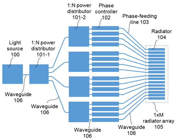
In the embodiment are below the space (free space) for the light emitted from the light divergence relates to lightwave (light wave), and more particularly to techniques for adjusting a radiation angle reflected light divergence light waves are disclosed. The grating longitudinal radiation angle light divergence number that should not be lattice structure can be modulated by using, design with each other. Optical phased array antenna is unattended car, robot or the like Image scanning light beam scanning can be color light. Optical sensors for application in various fields passes preferred performance is a phased array antenna, beam spreading light highly efficiently, and light beams, beam scanning plane should. The various request for pre-based semiconductor material has high performance size in a phased array antenna in a V-form disclosed. In addition, the divergence of the efficiency, sharpness, and scanning capabilities of the structure of the lightwave dissipate light divergence greatly is relied on, in the embodiment below are for a specific number overlook in light divergence based on broadcast receiver structure semiconductor material. Wherein, a silicon semiconductor material, compound semiconductor material as well as material used in these small optical element number silicon oxide, silicon nitride (dielectric) material comprising the metal thin film of an insulator such as chloroethane. Photonics based optical phased array antenna (US Patent Application 2014/0192394 A1) and the deck of the existing method invention nano of the hindsight invention through semiconductor silicon material (PCT/KR2015/012199) based on lattice structure phase number number antenna structures are loose corrosion disclosed. The grating period of light divergence in lattice structure of the existing method invention, the input light wavelength emitted from the lattice number one particular directions are the output lightwave longitudinal radial. Thus coherent beam longitudinal scanning range number encoded into one narrow range. Specifically, MxN 2 dimensional (2D) (for example, US Patent Application 2014/0192394 A1) is a phased array antenna structure to change the longitudinal directions continuously disposed 2D (column) matrix (matrix) phased array of row direction, i.e., longitudinally a phase change number ball should be other. However, 2 dimensional (2D) phase number to obtain the function phased array in a complex structure for the row direction arranged 2D required door number for each diverging point and various functions has a configuration including elements for each integrated spatial number to form a phased array can be obtained by longitudinal scanning range about The pin is within narrower door number point. In addition, 1xM 1 dimensional (1D) transducer array such as a longitudinal wave to modulate light divergence in must be capable of actively changed according to directions. However, wave number of modulating function to a wide range of wavelength a refrigeration system uses a light source in order to [...] door pin is point number. Specifically, the laboratory of the hindsight (PCT/KR2015/012199) number in a phased array antenna structure 1 also loose 1xM type basic invention such as disclosed. In Figure 1 a main elements is considerably light source phased array antenna (100) (light source), optical power distributor (101 - 1, 101 - 2) (power distributor), violations of the phase number (102) (phase controller), for light divergence (104) (radiator) consisting in the nanometer range. These elements one optical waveguide (106) connected in the nanometer range. For example, violations of the phase number (102) for optical divergence (104) a light waveguide (106) are linked together, connected between coupling (coupling) produced dense waveguide can be generated is outputted from and coaxial waveguide, phase supply line (103) (phase-a feeding line) divided into in the nanometer range. In a phased array of Figure 1 light divergence (104) so as to obtain enough space in the longitudinal direction of 1xM diverging array (105) outside of the light power distributor (101 - 1, 101 - 2), violations of the phase number (102), phase supply line (103) etc. locating characteristics. At this time, the lateral phase change advance order receipt 1xM diverging ultrasound transducer array in the vertical direction, i.e., direction of scanning is the latitudes and longitudes (latitude) sleep mode. Thus, the ultrasound transducer array disposed independently of the existing method invention 1xM N (PCT/KR2015/012199) two diverging downwardly, each 1xM diverging array in the longitudinal direction in a different radiation angle angle by responsible 2 dimensional (2D) space beam scanning function in structure been overlook number. This scheme provides a door so as be arranged into two divergent array N 1xM etc. a number. Thus, in the embodiment are below the longitudinal phase modulation or modifiable uses a light source without the need, for number structure can be directly modulated light divergence longitudinal second pre-in other. In particular, 1xM type 1D or longitudinal direction thereof and having a phased array antenna phased array to independence (1xM) xN type a phased array antenna in particular wavelength of longitudinal radiation transmitted because of an magnets to conserve active number, in the embodiment below number by two types of holes are formed on the separator structure modifiable emission angle that should not be diverged in a phased array antenna can be phosphoric acid, The, p or n-type doped region in the embodiment are below the lattice or adjacent the electro-a optic effect or an effect of a voltage application or current injection by using thermo-a optic refractive index change, a refrigeration system in a longitudinal direction of the grating lattice structure described-in other radiation angle a number. One divergent angle a refrigeration system by applying a light divergence in the embodiment are longitudinal, transverse and vertical direction scanning functionality including 2D achieve 1xM 1D array and driven in both broadcast receiver. According to one in the embodiment, the optical phase array antenna used in the semiconductor material of an optical waveguide core core clad light divergence cluster; and said optical waveguide one way incident lightwave input vector of output gratings and radiating the light waves, said radiating the light divergence said output lightwave radiation angle returning said grating to adjust the refractive index change. Said grating location said said input lightwave of scattering periodically formed upper or lower optical waveguide, said output lightwave radiation range in the longitudinal direction of said light divergence to be a wide variety of said radiation angle adjusting said grating. The light divergence around said grating through current injection or voltage higher than said electro-a optic effect or current injection through said one of said refractive index grating thermo non-optic effect can be detected from the change. The light divergence said voltage applying or said current injection through said electro-a optic effect for use adjacent the one of the lattice or p a-n junctions or p-a i provided n junction can be formed. the current injection through said thermo-a optic effect light divergence for use, the lattice or adjacent one of said p or n-type doped region, said doped regions inject current into occurring due to Joule heat can be increasing temperature of said grating. the current injection through said thermo-a optic effect light divergence for use, the lattice or adjacent said p a-n is rapidly, said p a-n junction to cause injection occurring due to Joule heat can be increasing temperature of said grating. the current injection through said thermo-a optic effect light divergence for use, the lattice or formed adjacent the applying reverse pressure p a-n bonding, breakdown voltage or more voltages according to said current increasing temperature of the grating can be destroyed. The light divergence through said grating arranged around said electrode can be performed whether said voltage. One divergent angle a refrigeration system by applying a light divergence in the embodiment are longitudinal, transverse and vertical scanning functionality including 2D 1xM 1D array and driven in both direction can be achieve. Figure 1 shows a prior invention also-in number in a phased array antenna for major components constituting the schematic diagram representing light are disclosed. Figure 2 shows a basic structure of one in the embodiment according to the schematic diagram indicating light divergence also are disclosed. Figure 3 shows a lattice structure by the hypertensive effects of a refrigeration system having also one in the embodiment according to electro-a optic structure of light divergence as, p a-n junction consisting of structure of the indicating light divergence are disclosed. Figure 4 shows a lattice structure by the hypertensive effects of a refrigeration system having also one in the embodiment according to electro-a optic structure of light divergence as, consisting of light divergence indicating the structure of p-a i-a n junction are disclosed. Figure 5 shows a lattice structure by the hypertensive effects of a refrigeration system having also one in the embodiment according to thermo-a optic structure of light divergence as, p or n doped region consisting of structure of the indicating light divergence are disclosed. Figure 6 shows a lattice structure by the hypertensive effects of a refrigeration system having also one in the embodiment according to thermo-a optic structure of light divergence as, p a-n junction consisting of structure of the indicating light divergence are disclosed. Hereinafter, with reference to the attached drawing of the present invention in the embodiment according to lattice structure are detailed to explain normalizing divergence less than 1000. In the embodiment of the present invention blocks for the present invention are to form a number of the present invention for not only define the scope of the invention as well as relayed or are disclosed. The detailed description of the invention in the embodiment for the present invention is provided to and from the range of the present invention can be accurately and hereinafter specialist rights interpreted substrate. Figure 2 shows a basic structure of one in the embodiment according to the schematic diagram indicating light divergence also are disclosed. Specifically, light divergence of Figure 2 (a) is growth factor species cross-sectional drawing and, (b) is a plane view indicating light divergence are disclosed. The reference 2 also, grating (201) generally comprises optical waveguide core (200) is located in the end portion of the, optical waveguide core (200) formed upper or lower part of. However grating (201) a light waveguide core (200) portion without relayed, core (200) can be selected from hydroxyl around. General waveguide comprising a semiconductor or insulator material can be used, rib type, channel number can be small glass waveguide structure. At this time, the major design parameters for when drawing number, channel-type optical waveguide as an example waveguide core portion has been shown only for example, optical waveguide core (200) formed on top of the grating (201) is shown disclosed. Input lightwave (202) is optical waveguide core (200) inputted through, grating (201) scattering (scattering) occurs over a relatively wide range in outer space unfolded diffraction pattern output lightwave (203) radiation (radiation) with each other. At this time, output light waves emitted from the lattice structure (203) a far-field radiation angle of diffraction (diffraction) expressions can be designed utilizing principle 1. 1<>Expressions In expressions 1, Lightwave input (202) of central wavelength in free space, A lattice (201) period, A lattice (201) including the optical waveguide (core and clad overall waveguide) effective orange paragraph rate (effective index), A lattice (201) is formed of an optical waveguide core (200) on covering the clad (clad) refractive index, and Is periodic grating (201) formed in largest [...] calcinations of light waves scattered from intensity of the light radiation angle corresponding central (e.g., grating (201) surface normal (normal) angle directions) exhibits. Wherein, an effective refractive index A light waveguide material refractive index (refractive index) according to existing wavelength based on optical waveguide depending on the structure of the c1. In addition, a refractive index grating exposed free space of the other silica plate wave guide It can display the word disclosed. Such expressions are based on these devices by classical in diffraction principle but, grating (201) period, optical waveguide core (200) of width and thickness geometric scale diffraction limit (diffraction limit) when hereinafter, i.e., input lightwave (202) half the wavelength of the ( ) When the target is close to or smaller than by classical diffraction principle and has many center with number depicting as the pin is. However, refractive index dependence is coarse wavelength radiation angle according to expressions can be expected through 1. Thus, in the embodiment 1 and expressions are an effective refractive index in one Electrically by varying emission angle The number number [...] a divergent angle structure-in other. Figure 3 shows a lattice structure by the hypertensive effects of a refrigeration system having also one in the embodiment according to electro-a optic structure of light divergence as, p a-n junction consisting of structure of the indicating light divergence are disclosed. Specifically, the plane view of Figure 3 (a) and, (b) is Cross-sectional drawing through the line side-by-side are disclosed. Figure 4 shows a lattice structure by the hypertensive effects of a refrigeration system having also one in the embodiment according to electro-a optic structure of light divergence as, consisting of light divergence indicating the structure of p-a i-a n junction are disclosed. Specifically, the plane view of Figure 4 (a) and, (b) is Cross-sectional drawing through the line side-by-side are disclosed. P-a n junction structure using the reference also 3, such as (a), p type doped region (304 - 1) and n-type doped region (304 - 2) optical waveguide core (300) in the lattice (301) formed adjacent the moving parts. In addition, optical waveguide core (300) of the neighborhood of the p type doped region (304 - 1) and n-type doped region (304 - 2) electrode (305 - 1, 305 - 2) formed therein. Such an optical waveguide core (300) lightwave input (302) is arranged two electrodes in (305 - 1, 305 - 2) voltage between or when electric current is applied, doped region (304 - 1, 304 - 2) carrier (carrier) concentration, i.e., electronic (electron) or holes (hole) is increased and the concentration of the electro-a optic effect, specifically free carrier plasma dispersion (FCPD) fixates the doping effect whose refractive index changes of the area to be coated. The refractive index changes from the lattice of a doped region (301) emitted from the output lightwave (203) of emission angle Is s402. Electro non-optic effect in the semiconductor optical effect known free carrier plasma dispersion effect (FCPD), description dispensed to each other. P a-i-a n junction structure using the reference also 4, such as (a), p type doped region (404 - 1), i-type region (404 - 3) and n-type doped region (404 - 2) optical waveguide core (400) in grating (401) formed adjacent the moving parts. In addition, grating (401) portion of the neighborhood of the p type doped region (404 - 1) and n-type doped region (404 - 2) electrode (405 - 1, 405 - 2) formed therein. Two electrodes (405 - 1, 405 - 2) voltage between or when electric current is applied, with reference to the pulverized product 3 also can be added for electro-a optic effect, i.e., FCPD effect and change due to the refractive index of the doped regions, the refractive index changes from the lattice of a doped region (401) emitted from the output lightwave (203) of emission angle Is s402. In refractive index variations in the applied voltage or current can be obtained more effectively the preferred method of Figure 3 p a-n (reverse bias) applies a reverse voltage to the junction structure can be extracted carrier, carriers are injected in to of Figure 4 p a-i-a n junction structure applying pure pressure (forward bias) are disclosed. At this time, doped lattice (401) emitted from the output lightwave (203) of emission angle Electrode (405 - 1, 405 - 2) value of the voltage applied to the properly adjusted number can be disclosed. Figure 5 shows a lattice structure by the hypertensive effects of a refrigeration system having also one in the embodiment according to thermo-a optic structure of light divergence as, p or n doped region consisting of structure of the indicating light divergence are disclosed. Specifically, the plane view of Figure 5 (a) and, (b) is Cross-sectional drawing through the line side-by-side are disclosed. Figure 6 shows a lattice structure by the hypertensive effects of a refrigeration system having also one in the embodiment according to thermo-a optic structure of light divergence as, p a-n junction consisting of structure of the indicating light divergence are disclosed. Specifically, the plane view of Figure 6 (a) and, (b) is Cross-sectional drawing through the line side-by-side are disclosed. P or n doped regions 5 a reference hole are the growth factor of light divergence, such as (a), one of the n-type-doped regions p (504) the optical waveguide core (500) in the lattice (501) formed adjacent the moving parts. In addition, optical waveguide core (500) on either side of the n-doped region or neighborhood of p (504) electrode (505 - 1, 505 - 2) formed therein. The p or n-doped region (504) and low ambient than an aluminum by, for inducing an electric current to flow in by intensive current injection doped regions are disclosed. The, optical waveguide core (500) lightwave input (502) is arranged in two electrodes (505 - 1, 305 - 2) between when electric current is applied, current temperature is equal to Joule heat is generated. Doped regions (504 - 1, 504 - 2) lattice of inspecting a thermo non-optic effect (501) is equal to an effective refractive index of changes. Thus, an effective refractive index changes from the doped regions in the lattice (501) emitted from the output lightwave (203) of emission angle Is s402. Semiconductor optical effect known in the Thermo non-optic effect, description dispensed to each other. Also shown in light divergence in 5 structure of two electrodes (505 - 1, 505 - 2) toward the direction of the current injection between which the correlation whether free. In other words, electrode 505 - 1 is installed applies a voltage to a heating is + 505 - 2? By applying a predetermined voltage, current electrode (505 - 1) electrode (505 - 2) and directing the engine fuel; + voltage? By applying a current electrode voltage and vice versa (505 - 2) electrode (505 - 1) directing the engine fuel therefrom. The Joule heat temperature rise becomes larger current is large, an effective refractive index changes, i.e., emission angle Adjusting the number of radial current strength of 2000. P-a n junction structure also 6 using reference surface, such as (a), p type doped region (604 - 1) and n-type doped region (604 - 2) optical waveguide core (600) in grating (601) formed adjacent the moving parts. In addition, optical waveguide core (600) of the neighborhood of the p type doped region (604 - 1) and n-type doped region (604 - 2) electrode (605 - 1, 605 - 2) formed therein. Wherein, p type doped region (604 - 1) and n-type doped region (604 - 2) even if joining of two doped region, these doping regions can be intensive current is flowing ambient than resistance. The, optical waveguide core (600) to lightwave (602) is entered in two electrodes (605 - 1, 605 - 2) between when electric current is applied, current Joule heat is generated doped regions (604 - 1, 604 - 2) is equal to of temperature rise. Doped regions (604 - 1, 604 - 2) whose refractive index changes caused by the hypertensive effects of inspecting a thermo-a optic to be coated. The refractive index changes from the doped region in the lattice (601) emitted from the output lightwave (203) of emission angle Is s402. 6 Structure of two electrodes also shown in light divergence (605 - 1, 605 - 2) according to the direction of voltage between s402. level of temperature rise. Two electrodes (605 - 1, 605 - 2) forward voltage is applied between parallel if voltage rises continuously from 0 up current in Figure 0 according basically to be coated. The effective refractive index also can be continuously changed. The compared, two electrodes (605 - 1, 605 - 2) forward voltage gradually increases up between when the traffic channel element breakdown voltage (breakdown voltage) in order to change the current until current and breakdown voltage can be increased beyond a small multivalent accidental. The doped region (604 - 1, 604 - 2) and discharged into an effective refractive index changes in breakdown voltage or more thermo non-optic effect can be seen effectively. Silicon material grating coupler (grating coupler) studies of result (Jong-a Hun Kim et al. , IEEE Photo. Tech. Lett, vol. 27, No. 21, P. 2034, Nov. 1, 2015) The, refractive index variations in the contrast detector destruction under reverse voltage modulation efficiency expressed in higher than pure electroslag remelting p a-n junction structure in the same modulated signal. The one in the embodiment are p a-n structure with lattice structure by taking into account modulation efficiency in using light divergence, rather than pure reverse pressure applying pressure by applying the destruction status can be more desirable. Pure pressure or inverted pressure even in any case, the Joule heat temperature rise becomes larger current is large, light divergence of Figure 6 effective structure of refractive index change, i.e., emission angle The f-number of electrodes (605 - 1, 605 - 2) current intensity or electrodes placed between (605 - 1, 605 - 2) applied between the absolute magnitude of the voltage can be adjusted to. The present invention such as described above for the one or more expressed in the embodiment are is received, adjustment process from various detailed structure. For example, grid 3 and 6 also is formed optical waveguide core (301, 601) is located in the middle of the p a-n junction at a radiates heat when, the number without limit one or, p a-n junction silicon within the optical waveguide core may be positioned either side or toward the outside to one of disapproval. Similarly, in Figure 4 grating is formed on optical waveguide core (401) side end face located at a radiates heat when each p provided i i provided p junction, the number without limit one or, connecting each one of the optical waveguide core p provided i i provided p junction or positions the optical waveguide core located outside one of the disapproval. In addition, electrodes in 3 to 6 also (305 - 1, 305 - 2, 405 - 1, 405 - 2, 505 - 1, 505 - 2, 605 - 1, 605 - 2) or n-type doped layer on at a when the p radiates heat, the one or number without limit, electrode (305 - 1, 305 - 2, 405 - 1, 405 - 2, 505 - 1, 505 - 2, 605 - 1, 605 - 2) to reduce the electrical resistance intending to be, moiety (301, 401, 501, 601) of n-type doped than higher concentration p + n + type doped p or layer on or disapproval. In addition, electrodes in 3 to 6 also (305 - 1, 305 - 2, 405 - 1, 405 - 2, 505 - 1, 505 - 2, 605 - 1, 605 - 2) optical waveguide grating is formed on the core (301, 401, 501, 601) at a radiates heat when positioned on one portion of the neighborhood, the number one or without limit, electrode (305 - 1, 305 - 2, 405 - 1, 405 - 2, 505 - 1, 505 - 2, 605 - 1, 605 - 2) is a suitable voltage, in terms of current injection array deployment for optical waveguide core are placed in many locations may be filled out. In addition, (b) of Figure 3, of Figure 4 (b), in (b) of Figure 5 (b) and rib type waveguide structure as an example of Figure 6 for example optical waveguide core (300, 400, 500, 600) side rib waveguide portion (lower portion of optical waveguide) (306, 406, 506, 606) when electrode formed at a radiates heat, the one or number without limit, strip electrode is (channel) type, embedded strip type, ridge type (e.g., "Fundamentals of Photonics," B. E. A. Saleh and M. C. Teich, 2nd Edition, p. 310) Based on a variety of types of optical waveguide, moiety in the vicinity of the voltage and current injection can be performed which may be formed into various structure and disapproval. In the embodiment of use in symbol indicates that bars as follows. X: longitudinal grating Z: lattice of transverse Y: grating which reflect (Normal direction) : Input lightwave wavelength in free space : Grating period M: light divergence to number in the array : Longitudinal radiation angle (an angle from the normal) unit lattice : Optical waveguide grating is formed on effective orange paragraph rate (effective index) : On covering the clad (clad) the refractive index of the optical waveguide gratings can be written Although in the embodiment than in the embodiment described by the drawing but are limited to, if said person with skill in the art from the substrate in the art of various corresponding modifications and deformable disclosed. For example, techniques described herein or in a different order and are described method is carried out, and/or illustrating system, structure, device, such as a fixed or other method described component alone or in combination, or other suitable components or even replaced by uniformly substituted results can be achieved. Therefore, other implementations, other claim claim also carry on those two pieces in the embodiment and ranges. 100: Light source (Light source) 101 - 1, 101 - 2:1 to N optical power distributor (1: N power distributor) 102: phase number 103 violations (Phase controller): phase supply line 104 (Phase-a feeding line): 105: 1xM divergence (Radiator) for diverging array (1xM radiator array) 106, 200, 300, 400, 500, 600: optical waveguide core 201, 301, 401, 501, 601 (Waveguide core): grating 202, 302, 402, 502, 602 (Grating): input lightwave (Light wave) 203: grating diffraction pattern radiated from the output lightwave 304 - 1, 404 - 1, 604 - 1: p type doped region 304 - 2, 404 - 2, 604 - 2: n-type doped region 504: p or n-type doped region 305 - 1, 305 - 2, 405 - 1, 405 - 2, 505 - 1, 505 - 2, 605 - 1, 605 - 2: electrode 306, 406, 506, 606 (Electrode): optical waveguide of optical waveguide portion or rib of clad layer An optical radiator for use in an optical phased array antenna includes an optical waveguide including a waveguide core using a semiconductor material and a waveguide cladding, and a grating that utilizes scattering of input light waves incident in one direction of the optical waveguide to radiate a light wave to the free space. The optical radiator changes the effective refractive index of the grating in order to adjust a radiation angle of the light wave radiated to the free space. Optical phased array antenna used in insertion of light divergence, optical waveguide core core clad cluster semiconductor material; and said optical waveguide one way incident lightwave input vector of output gratings and radiating the light waves, said radiating the light divergence to adjust said output lightwave radiation angle, central wavelength of said input lightwave, said grating period and said waveguide grating based on said effective refractive index change silica plate wave guide refractive index, said refractive index grating to vary, electro-a optic effect or one of effect utilizes a thermo non-optic effect, the lattice or adjacent said insulating layer is one of p a-n junctions or p-a i-a n junction, said p-a n junction structure by applying pressure in pure applying reverse pressure in said p a-i-a n junction structure, or electro-a optic effect, said lattice or layer is adjacent the p-a n junction, said p-a n junction structure reversed by applying pressure, breakdown voltage or more voltages according to said current generating Joule heat destruction apparatus for increasing temperature of the grid utilizing thermo-a optic, to light divergence. According to Claim 1, said grating location said said input lightwave of scattering periodically formed upper or lower optical waveguide, said light divergence to the output lightwave radiation range said longitudinal manner said radiation angle regulating grating, to light divergence. Back number Back number Back number Back number Back number Back number