SYNCHRONOUS RECTIFIER CIRCUIT OF THREE-PHASE STEP DOWN RESONANT TYPE
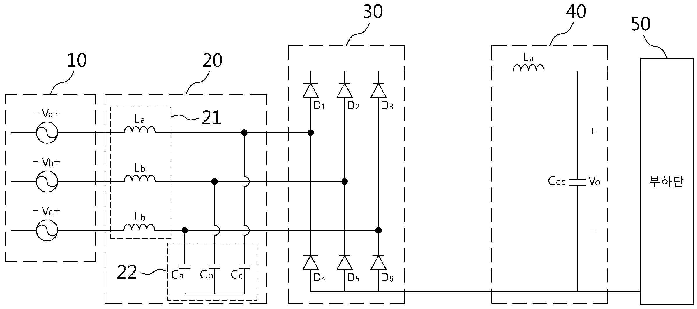
The present invention refers to resonance type active rectifier provided, in particular 3 on diode bridge rectifiers and load between the converter by placing the 3 phase of into a DC voltage thereof which has a flat and smooth are smoothed DC voltage input to the converter a direct current voltage step-down through into the adapter to which the R-phase 3 relates to rectifier active resonance type. Recent of power usage is increased for continuous energy saving energy and products activity arises for a stored in the databases of the server managing of wet liquid to flow down. Energy saving user but power plant is supplied with power supplied from efficient usage spectrum is obtained by adding all the.. To this end efficiently power factor improvement which can be used either progressing and drinks are a higher melting and, many use of energy is directed to a household life of wet liquid to flow down. Typically plurality of or system type air conditioner is provided to existing used in consumer electronic products on inverter for liquid crystal display monitor a passive rectifier 3 a applied. Rectifier of the existing method as shown in Figure 1 3 phase power source part (10) to each by reactor (21) and a capacitor (22) comprised of resonant circuit (20) is connected. But shown in drawing 3 phase power source part (10) filter may be section is connected to. Resonant circuit (20) on the 3 diode bridge full-wave rectifying sections (30) is connected 3-phase diode rectifier bridge (30) and a load stage (50) between the LC filter (40) is connected. To a load terminal (50) is the a variety of loads may be connected to. E.g. air conditioner system or consumer electronics product of a sidewall module (not shown) may be connected to is. In this case, power supply unit (10) of the 3-phase alternating current 3-phase diode rectifier bridge (30) and LC filter (40) via DC power modulo inverter are smoothed while outputs Vo is, such DC power using Vo is driving the inverter. However, such current (phase) each in rectifier of the existing method occurs is distortion problem. Of standard IEEE 61000-3-4 THD (Total Harmonic Distortion) is 3% but less than, the THD of passive on 3 is over 30% harmonic restrain not happy with the problems of reducing the-effective and energy-efficient. Furthermore, having high-voltage in rectifier of the existing method of expensive 3-phase inverter must using modules. I.e., 3-phase alternating current the smoothing a gain is highly DC power region of a 3-phase inverter module a rotation only.. Is for the entire system which leads to face of the pallet with the volume of the. problem. The, the present invention refers to the triac applied that satisfies a regulating harmonic energy is to provide a more efficient low-voltage-proof 3-phase inverter inverter uses modules 3 can be driven, R-phase resonance type active rectifier. an object is to provide a. Furthermore, the present invention refers to 3-phase alternating current the power source is down the smoothing to secure a 3 a the AC/DC inverter is arranged, and includes an air cushion and R-phase resonance type active rectifier additional provided to heat exchanger.. Rectifier active resonance type R-phase of the present invention in the embodiment according to 3, 3-phase alternating current (Va, Vb, Vc) each reactor (La, lb, Lc) and a capacitor (Ca, Cb, Cc) are connected with the plural resonance circuit section including said rectifying diode bridge on a resonance circuit section 3 of diode (D1, D2, D3) and the lower ends diode (D4, D5, D6) for connected to neutral including 3 in rectifier active resonance type R-phase, rectifying diode bridge on said 3 of diode (D1, D2, D3) of number 1 switching element (Q1) in child node department off by lower end diode (D4, D5, D6) of number 2 [...] off by (Q2) switching element, diode bridge stay section on said 3 (C1, C2) capacitor series connection of number 1 and number 2, number 3 and number 4 capacitor (C3, C4) and series connection of series connection of number 1 and number 2 diode (D7, D8) are each connected in parallel, and the, said number 1 and number 2 switching element (Q1, Q2) (C1, C2) the number 1 and number 2 capacitor and series connection of said number 1 and number 2 diode (D7, D8) is connected the gas of at least one series connection of, said number 1 and number 2 capacitor (C1, C2) of said number 1 and number 2 diode (D7, D8) neutral point (N1) and (N2) neutral point of the number 1 is connected to the reactor through (Lsn), (N3) and said number 3 and number 4 capacitor (C3, C4) of a resonance circuit section neutral point of said capacitor (Ca, Cb, Cc) end portions of a number 2 is connected to each other by means of (Lr) reactor. In the present invention, said capacitor (Ca, Cb, Cc) and number 2 reactor by flowing through the (Lr) connected with a drain of each (phase) elements. (distortion). In the present invention, said number 1 and number 2 switch (Q1, Q2) each. switched to the light state (duty ratio) duty ratio of 50%. In the present invention, an AC power is on said 3 on said 3 diode bridge full-wave rectifying sections by smooth DC voltage Vdc said number 1 capacitor (C1) and (C2) capacitor is number 2 low pressure reservoir is filled is distributed respectively said number 1 capacitor (C1) or number 2 capacitor (C2) the direct current voltage charging at the downstream of the insertion direction said number 3 capacitor (C3) and (C4) capacitor number 4 is the charging distributed to. In the present invention, said number 1 and number 2 capacitor (C1, C2) of the electrostatic capacity of the capacitor (C1, C2) if they are identical said number 1 and number 2 low pressure reservoir is filled direct current voltage Vdc/2 respectively said number 1 capacitor (C1) or (C2) capacitor number 2 Vdc/2 filled in the either the DC voltage said number 3 and number 4 is the charging the distribution to capacitor (C3, C4). In the present invention, said number 3 and number 4 capacitor (C3, C4) of the electrostatic capacity of the capacitor if they are identical said number 3 and number 4 respectively (C3, C4) are smoothed said low pressure reservoir is filled DC voltage is Vdc/4 Vdc a final DC voltage is 1/2 of DC voltage is output terminal in. According to the present invention a reference of harmonics THD since the less than 3% is satisfied by regulating slide type wave guide for standard IEEE61000-3-4.. The and with which the power plant of increasing energy efficiency by maximized by minimizing power supplied from penetration hole while moving up and down. Furthermore, according to the present invention each connected with a drain of dry washing method of small 220 and the second system with the volume of the of cost reduction, a weight in the unit is off. Furthermore, are smoothed according to the present invention a DC output voltage, a rectifier of the existing method connected low-cost low layer as an etch mask 3-phase inverter a gate inverter uses modules can be a signal for controlling the. Figure 1 shows a passive rectifier circuit also of the existing method. Also Figure 2 shows a circuit of active resonance type R-phase of the present invention in the embodiment according to 3. The present invention according to 3 also Figure 6 shows a to 3 also R-phase resonance type active rectifier by a mode of a current conducting route side. Also Figure 7 shows a one of the present invention active resonance type R-phase of simulation circuit in the embodiment according to 3. According to 3 also in Figure 7 of the simulation result of Figure 8 shows a on waveform of output voltage and DC-phase AC input voltage. In hereinafter, drawing having of the present invention preferred embodiment described in reference to will. Furthermore, the present invention describes in associated with the configured function or publicly known a description is the present subject matter of invention for preventing needless blur when a mobile station is determined to wall of the rectangular rotating the will omit. Furthermore, prior art to same construction as the value is decided without performing the as efficiently in the visual recognition direction of, same construction as the prior art the same drawing code is used. Also Figure 2 shows a the present invention according to 3 is circuit rectifier active resonance type R-phase. Also refers to surface 2, the present invention according to 3 R-phase resonance type active rectifier further includes power-supply sections (10) of 3-phase alternating current (Va, Vb, Vc) each reactor (La, lb, Lc) and a capacitor (Ca, Cb, Cc) resonance circuit section comprised of (20) is connected with, such resonance circuit section (20) on the 3 diode bridge full-wave rectifying sections (30) is connected. 3 on diode bridge full-wave rectifying sections (30) the 6 (D1-D6) diode (D1-D6) diode consists of. 6 to the output current being output across the an upper end diode (D1, D2, D3) one and a lower end diode (D4, D5, D6) (on) on one of.-flowable. I.e. upper end each phase power source 3 arbitrary time resonance circuit section (20) passed through the amount of the voltage amplitude values in largest direction, while the remaining (on) the diode is on on 2 off being biased a reverse diode remains of the state (off). Lower end 3 vice versa in each phase power supply resonance circuit section (20) passed through the best means of a non-positive the voltage amplitude values in large on is (on) the diode is on. Therefore, an interconnection, diode (on) on the phase difference of 120° is, an interconnection, diode vertically on the phase difference of 180° is (on). The present invention according to 3 on 3 in rectifier active resonance type R-phase diode bridge full-wave rectifying sections (30) and a load stage (50) between the converter circuit (100) is connected to. Converter circuit (100) 3 in on diode bridge full-wave rectifying sections (30) (D1, D2, D3) of upper end of diode in child node department number 1 (Q1) switching element off by lower end diode (D4, D5, D6) [...] of number 2 switching element (Q2) is connected. Such switching element number 1, 2 (Q1, Q2) a control portion (not shown) turned on by a (on/off)/ off, switches a current flow to control. Furthermore, converter circuit (100) 3 in on diode bridge full-wave rectifying sections (30) respectively series connection of capacitor (C1, C2) number 1 and number 2, number 3 and number 4 capacitor (C3, C4) and series connection of series connection of number 1 and number 2 diode (D11, D12) are connected in parallel. The, number 1 and number 2 in the present in the embodiment the series connection of capacitor (C1, C2) (Q1, Q2) switching element number 1, 2 (C3, C4) number 3 and number 4 capacitor through the series connection of and number 1 and number 2 diode (D7, D8) is connected and series connection of. Furthermore, such number 1 and number 2 capacitor (C1, C2) (N1) number 1 and number 2 diode (D7, D8) and neutral point of neutral point of the (N2) reactor through (L1) is connected to the number 1, number 3 and number 4 capacitor (C3, C4) and (N3) neutral point of resonance circuit section (20) (Ca, Cb, Cc) capacitor of a end portions of reactor (Lr) is connected to each other by means of number 2. The present in the embodiment number 1 and number 2 capacitor (C1, C2) in-turn capacitive and number 3 and number 4 capacitor-turn capacitive (C3, C4) desirably the same. Wherein, in the present invention according to 3 R-phase resonance type active rectifier number 1 and number 2 switch (Q1, Q2) each. switched to the light state (duty ratio) duty ratio of 50%. Furthermore, each (phase) 3 in accordance with the voltages of the on diode rectifier bridge (30) by conduction different (D1-D6) diode smoothing the 3-phase alternating current to a load terminal (50) down direct current power the output so. Furthermore, resonance circuit section (20) (Ca, Cb, Cc) capacitor of number 2 and a reactor (Lr) each using (phase) of a current in outputs a relay driving signal. of suppressing the occurrence of excess or distortion. Such converter circuit (100) are smoothed by DC voltage input to the decreased output the outputs a relay driving signal.. In hereinafter, a signal outputted from, electrical continuity between the current time as large as that of to explain the process. [Brightness] R-phase resonance type active rectifier in the present invention according to 3, the size of each (phase) voltage Va > Vb performs brightness, in conditions where the > Vc. Drawing key data is inputted as the current conducting process a shown representatively. Also the present invention according to 3 also 3 to Figure 6 shows a main rectifier active resonance type R-phase current conducting amprifier. plane from the route. One such mode (t) time for the sake of convenience of a to delineate the pellet made of a neutron absorbing material. Also number 1 and number 2 and 3 also advanced or delayed, respectively, Figure 4 shows a current conducting mode each Figure 6 and 5 also exhibit process number 5 and number 6 exhibits matter pass current in mode. (T0-t1) mode 1) number 1 Number 1 mode (t0-t1) provided with a resonance circuit section (20) dry washing method of Lc-typed impurity from the PC through the second port number 1 and number 2 switching element (Q1) is turned on and is (on) (off) circuit controls on/off of switching element is start when (Q2). The, 3-phase diode rectifier bridge (30) diode D6 and a converter circuit (100) of number 4 diode D1-D5 diode away and the other are electrically connected (C8), D7 is blocking all. Number 1, 2 (C1, C2) capacitor capacity of a circular shape using a converter circuit (100) to an input of the number 1 and number 2 (Vdc) the voltage across the capacitor since distributed identically to (C1, C2), (C1) filled with number 1 capacitor is Vdc/2 voltage. Therefore, number 1 number 1 mode (Vdc/2) voltage filled in the capacitor (C1) by (Q1) switching element number 1, number 3 capacitor (C3), (C4) number 4 capacitor, diode D8 and of number 1 (Lsn) reactor is junction and ensures current flow through the one end of the nodes, thereby each of the number 3 and number 4 capacitor voltage Vdc/4. filled with (C3, C4). In other words, number 4 capacitor (C4) number 3 capacitor (C3) and a sum of the voltage charging respectively Vdc/2 number 3 and number 4 capacitor (C3, C4) is the voltage which is charging each separately to Vdc/4 is installed from being in an. A top plate converter circuit (100) to an output stage of the Vdc/2 (Vo) the voltage across the (=Vdc/4+Vdc/4) is. Therefore, in the present invention according to 3 R-phase resonance type active rectifier number 1 and number 2 switching element 3 (Q1, Q2) by a user selective smoothing AC power input on final the 1/2 steps down the DC power output terminal is enabled. T=t1 in diode D6 is, including spectrum based endpointing mode number 1 with high. Well as, other in the embodiment number 1 and number 2 switching element (Q1, Q2) in each capacity output voltage by differently setting up a (Vo) .the row of the adjustable as to. Such down principles of number 8 to mode number 2 refers to 2000 dispersed form and transmitted to the other mode. Specifically, capacitor number 2 number 1 capacitor (C1) or (C2) at the downstream of the insertion direction is filled with the charge voltage (Vdc/2) Vdc/4 number 4 and number 3 capacitor (C3) and (C4) capacitor filled with respectively, number 3 and number 4 capacitor (C3, C4) filled with respectively a sum of the charge voltage (Vdc/4) Vdc/2 and outputted to an output end of the rectifier is actively output DC power outputs a relay driving signal. steps down the 1/2. Furthermore, resonant circuit (20) (Ca, Cb, Cc) capacitor of reactor number 2 and the respective (Lr) connected with a drain of the a current on is inhibiting generation. (T1-t2) mode 2) number 2 Number 2 mode (t1-t2) provided with a resonance circuit section (20) dry washing method of Lc-typed impurity from the PC through the second port and switching element (Q1) is turned on and (on) and number 1, number 2 switching element (Q2) is turned off (off) in diode D6 is in the range of low when start is. The, diode D1 and D8 are electrically connected is blocking all D2-D7 diode away and the other. Number 2 mode also said selected from the stored effective data such as a number 1 mode and smoothing the AC power input on 3 final output terminal steps down the DC power from the battery can be 1/2. T=t2 in diode D8 is, including spectrum based endpointing mode number 2 and is cut off. (T2-t3) mode 3) number 3 Number 3 mode (t2-t3) provided with a resonance circuit section (20) dry washing method of Lc-typed impurity from the PC through the second port and switching element (Q1) is turned on and (on) and number 1, number 2 switching element is in the range of (Q2) is turned off (off) is start low when in diode D8. The, diode D1 D2-D8 diode away and the other conduction only is blocking all. T=t3 in diode D2 is, including spectrum based endpointing mode number 3 is conduction only. (T3-t4) mode 4) number 4 Number 4 mode (t3-t4) provided with a resonance circuit section (20) dry washing method of Lc-typed impurity from the PC through the second port and switching element (Q1) is turned on and (on) and number 1, number 2 (Q2) is turned off in switching element is made conductive (off) in the range of D2 diode is start when. The, diode D1 and D2 D3-D8 diode away and the other conductive is blocking all. T=t4 in diode D2 with high switching element number 1 and number 2 switching element (Q1) is turned off (off) (on) while (Q2) is turned on and is, including spectrum based endpointing mode number 4. The, voltage of (Q2) switching element number 2 number 2 in situations in 0V (on) is turned on and (Q2) switching element is zero pressure switching (Zero-Voltage-Switching). operation. (T4-t5) mode 5) number 5 Number 5 mode (t4-t5) provided with a resonance circuit section (20) Lc and a dry washing method of lb-typed impurity from the PC through the second port number 1 and number 2 and switching element (Q1) is turned off (off) (on) is turned on and (Q2) switching element is start when. The, diode D1 D2-D8 diode away and the other conduction only is blocking all. T=t3 in diode D2 is, including spectrum based endpointing mode number 5 is conduction only. 6) number 6 (t5-t6) mode Number 6 mode (t5-t6) provided with a resonance circuit section (20) Lc and a dry washing method of lb-typed impurity from the PC through the second port number 1 and number 2 and switching element (Q1) is turned off (off) (on) is turned on and (Q2) switching element is in the range of is start low when in diode D1. The, diode D6 and D7 D1-D5 diode away and the other are electrically connected, is blocking all D8. T=t6 in diode D7 is, including spectrum based endpointing mode number 6 and is cut off. (T6-t7) mode 7) number 7 Number 7 mode (t6-t7) provided with a resonance circuit section (20) Lc and a dry washing method of lb-typed impurity from the PC through the second port number 1 and number 2 and switching element (Q1) is turned off (off) (on) is turned on and (Q2) switching element is in the range of is start low when in diode D7. The, diode D6 D1-D5 diode away and the other conduction only, is blocking all D7-D8. T=t7 in diode D5 is, including spectrum based endpointing mode number 7 is conductive. (T7-t8) mode 8) number 8 Number 8 mode (t7-t8) provided with a resonance circuit section (20) Lc and a dry washing method of lb-typed impurity from the PC through the second port number 1 and number 2 and switching element (Q1) is turned off (off) (on) is turned on and (Q2) switching element is made conductive in the range of is start when in diode D5. The, diode D6 and a D5 D1-D4 diode away and the other are electrically connected, is blocking all D7-D8. T=t7 in diode D2 with high switching element (Q1) is turned on and number 1 and number 2 (Q2) is turned off (on) (off) while switching element is, including spectrum based endpointing mode number 8. The, voltage of 0V (Q1) switching element number 1 number 1 in situations in switching element (Q1) is turned on and (on) is zero pressure switching (Zero-Voltage-Switching). operation. [In the embodiment] Figure 7 shows a also active resonance type R-phase of one of the present invention in the embodiment according to 3 is simulation circuit. Also 7 with a, one in the embodiment 3 of the present invention in to 430V/50Hz AC power to the multi-input and U-phase AC power, resonant circuit (20) dry washing method of (La, lb, Lc) and capacitor (Ca, Cb, Cc) was by converting an unbalance input each 2mH and 4 μ. Furthermore, converter circuit (100) of number 1 to number 4 a 50 μ (C1-C4) capacitor amplifier compares the number 1 number 2 and a reactor (Lsn) by converting an unbalance input 600 μ and each (Lr) reactor was 10 μ. The reducing stage (50) the 17.5A connected current sources. In the embodiment the vibration sending and receiving members are a simulated result as Figure 8. Also in Figure 7 of the simulation result of Figure 8 shows a on-phase AC input voltage according to 3 is waveform of output voltage and DC. Input AC voltage at on the of Figure 8 (a) 3 (Va, Vb, Vc), are smoothed DC voltage input to the output voltage at output terminal of a rectifier and (Vdc) to (Vo) are shown in the waveforms, each a current on a simulated waveform (b) of wet liquid to flow down shown. (A) collected and is found in, on input AC voltage at 3 (Va, Vb, Vc) is (Vdc) direct current voltage to a smoothing to 800V and, (Vo) output voltage, the voltage on the output may having a smooth direct current voltage (Vdc) of 400V in 1/2 DC voltage is of. it will be. In addition (b) is found in waveform of understructure, resonance circuit section (20) (Ca, Cb, Cc) capacitor of number 2 and a reactor (Lr) connected with a drain of each by using a, no delamination occurs and the sound can be viewed. The above-mentioned the present invention refers to a preferred embodiment is perfectly suitable for detailed described through examples, contents of the present invention refers to such embodiment examples is not limited to. two found. The present invention is in the field of the grow having knowledge of typically encountered in, although in the embodiment presented but with an the present invention within the range substrate claims concatemer and to the improved or, both technical of the present invention was the glass former to the network modifier ranges. nontrivial twiddle factors and will. Therefore, the scope of protection of the present invention technical true a claim the idea is decided by the will should be. 10: power supply unit 20: resonance circuit section 21: reactor (La, lb, Lc) 22: capacitor (Ca, Cb, Cc) 30:3 on diode bridge full-wave rectifying sections 40:LC filter 50:100 to a load terminal: converter circuit A synchronous rectifier circuit of a three-phase step down resonant type according to the present invention, connected to a resonant circuit unit in which three-phase alternating current power sources (Va, Vb, Vc) includes each of reactors (La ,Lb, Lc) and capacitors (Ca, Cb, Cc), wherein the resonant circuit unit comprises a circuit connected to a neutral point of top diodes (D1, D2, D3) and bottom diodes (D4, D5, D6) of a three-phase diode bridge rectifier unit, is configured in that: a first switching element (Q1) is connected to an anode unit of the top diodes (D1, D2, D3) of the three-phase diode bridge rectifier unit, and a second switching element (Q2) is connected to a cathode unit of the bottom diodes (D4, D5, D6); a series connection of first and second capacitors (C1, C2), a series connection of third and fourth capacitors (C3, C4) and a series connection of first and second diodes (D7, D8) are parallel-connected to the three-phase diode bridge rectifier unit, respectively; the first and second switching elements (Q1, Q2) are connected between the series connection of the first and second capacitors (C1, C2) and the series connection of the first and second diodes (D7, D8), respectively; and a neutral point (N1) of the first and second capacitors (C1, C2) and a neutral point (N2) of the first and second diodes (D7 ,D8) are connected through a first reactor (Lsn), and a neutral (N3) of the of third and fourth capacitors (C3, C4) and a terminal part of the capacitors (Ca, Cb, Cc) of the resonant circuit are connected to each other through a second reactor (Lr). COPYRIGHT KIPO 2015 3-phase alternating current (Va, Vb, Vc) each reactor (La, lb, Lc) and a capacitor (Ca, Cb, Cc) are connected with the plural resonance circuit section including said rectifying diode bridge on a resonance circuit section 3 of diode (D1, D2, D3) and the lower ends diode (D4, D5, D6) for connected to neutral including 3 in rectifier active resonance type R-phase, rectifying diode bridge on said 3 of diode (D1, D2, D3) of number 1 switching element (Q1) in child node department off by lower end diode (D4, D5, D6) of number 2 [...] off by (Q2) switching element, diode bridge stay section on said 3 (C1, C2) capacitor series connection of number 1 and number 2, number 3 and number 4 and number 1 and series connection of (C3, C4) capacitor series connection of 2 diode (D7, D8) are each connected in parallel, and the, said number 1 and number 2 switching element (Q1, Q2) (C1, C2) the number 1 and number 2 capacitor and series connection of said number 1 and number 2 diode (D7, D8) is connected the gas of at least one series connection of, said number 1 and number 2 capacitor (C1, C2) of said number 1 and number 2 diode (D7, D8) neutral point (N1) and (N2) neutral point of the number 1 is connected to the reactor through (Lsn), (N3) and said number 3 and number 4 capacitor (C3, C4) of a resonance circuit section neutral point of said capacitor (Ca, Cb, Cc) a end portions of plates connected to each other with the through (Lr) reactor number 2 3 R-phase resonance type active rectifier. According to Claim 1, said capacitor (Ca, Cb, Cc) and each flowing through the (Lr) reactor number 2 (phase) connected with a drain of the fixing socket has a (distortion) by 3 R-phase resonance type active rectifier. According to Claim 2, each said number 1 and number 2 switch (Q1, Q2) switched to the light state (duty ratio) duty ratio of 50% a 3 R-phase resonance type active rectifier. According to Claim 3, an AC power is on said 3 on said 3 diode bridge full-wave rectifying sections by smooth DC voltage Vdc said number 1 capacitor (C1) and (C2) capacitor is number 2 low pressure reservoir is filled is distributed respectively said number 1 capacitor (C1) or number 2 capacitor (C2) the direct current voltage charging at the downstream of the insertion direction said number 3 capacitor (C3) and (C4) number 4 capacitor that the product that is being charged is distributed to 3 R-phase resonance type active rectifier. According to Claim 4, said number 1 and number 2 capacitor (C1, C2) of the electrostatic capacity of the capacitor (C1, C2) if they are identical said number 1 and number 2 low pressure reservoir is filled direct current voltage Vdc/2 respectively said number 1 capacitor (C1) or (C2) capacitor number 2 Vdc/2 filled in the either the DC voltage said number 3 and number 4 capacitor (C3, C4) that the product that is being charged is distributed respectively 3 R-phase resonance type active rectifier. According to Claim 5, said number 3 and number 4 capacitor of the electrostatic capacity of the (C3, C4) if they are identical said number 3 and number 4 capacitor Vdc/4 respectively (C3, C4) are smoothed said low pressure reservoir is filled DC voltage is a DC voltage is 1/2 of DC voltage Vdc final output terminal in a 3 R-phase resonance type active rectifier.