DISPLAY DEVICE
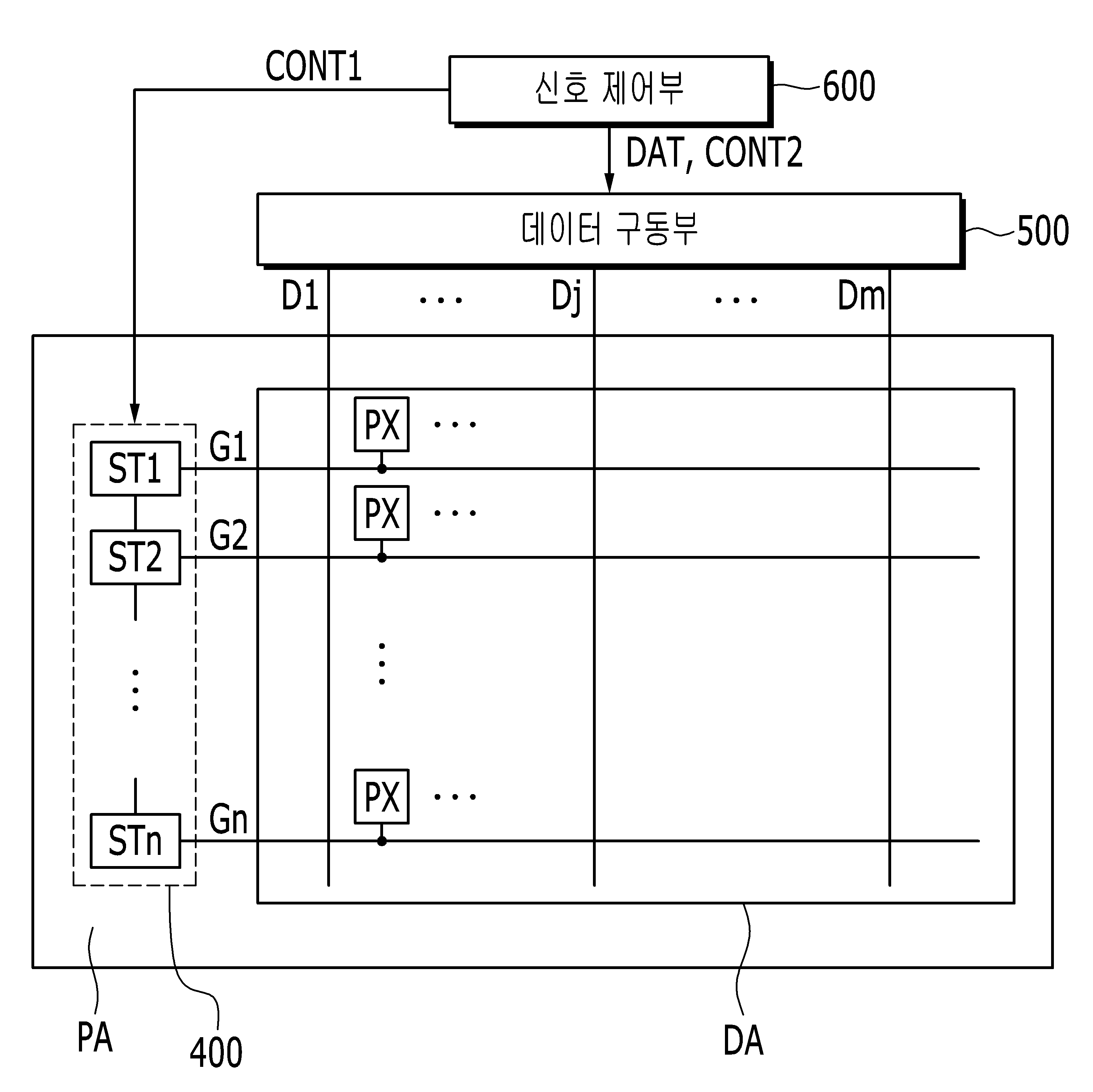
The present invention refers to display device relates to, a gate driver more particularly relates to including display device. Display device switching element generally including source and drain is connected to the display signal line dm is with array panel, display signal line gate line gate signal of pixels gate driver timing mode selection turn-on switching element, data lines data driver applying a voltage data, controlling and balance includes a control signal or the like. Display device during liquid crystal display device a message of a typical message one of the all--time as one of flat panel display device, pixel transistor and the inserted between the electrode (field generating electrode) is formed of the array panel therebetween that liquid crystal layer including an. Liquid crystal display device an electric field generating electrode by applying a voltage to the liquid crystal layer is adapted to generate an electric field and is easy to liquid crystal layer for determining the orientation of a liquid crystal molecules are polarization of incident light to display an Image by controlling the.. Transmittance of liquid crystal display device way helps to control are well a common. can be increased. Is of each pixel of liquid crystal display device including at least one pixel electrode, gate lines and data lines such as signal lines are arranged on which are in communication with the switching element and connected thereto. Thin film switching element such as a transistor three-stage electron device data as transmits it to a pixel electrode voltage. Liquid crystal display device, which generate an electric field in liquid crystal layer pixel electrode and the common electrode is formed the switching element adjusts the sign board to the and can comprise of. The liquid crystal device at least one electrode and the common electrode of pixels a plurality of may include a. Liquid crystal layer when an electric field is created a passivation layer an caused by the field of ITO and have a slit pattern electrodes is determined are the same. Such as a gate and data reproduced in the form of the integrated circuit chip, which driving circuit device to which are mounted, flexible printed circuit film (flexible printed circuit film) is mounted over the device is attached to and reproduced in the form of TCP (tape carrier package), printed circuit board (printed circuit board) may be mounted on. However, the thin film transistor channel high mobility and a method for the gate driving uncoated chip is connected the upper end of a sidewall which is not subject to signal lines are arranged on switching device means of the same process in a structure is integrated sign board is.. Such a gate driver dependently connected to a plurality of stages a shift register and a direct type backlight unit includes the plurality of signal lines. Plurality of stage includes and capacitor plurality of thin film transistors. Each stage receives either a a corresponding gate line is connected with the, ensures that the number of stages that a defined class each gate sequentially order outputs the gate signal line. Gate driver in device display be integrated in a sign board is, gate driver timing at which a video is displayed in a zone occupied by the non-display area is is mostly when the. Gate causes the drive to be the region of the lower array panel non-display region, in particular at which a video is displayed is display area peripheral region the increased area of the peripheral area for surface of small display device can't-extracting condition set by composed of the customer's identification code. The present invention is the problem of array panel in by reducing the area occupied by a gate driver display device to reduce an area of a peripheral region of.. If the second voice is inputted, the present invention another a array panel gate causes the drive to be while reducing transistor and a plurality of NMOS of the gate driving unit according WIPO structure by a rope.. Larger than the second panel a device embodiment of the present invention a plurality of pixels is located a display region and peripheral region of said display region including array panel, said peripheral located in the region the transistor and capacitor includes gate driving including, said transistor which is arranged in the upper portion said number 1 the second substrate, to form the. is superposed on said transistor. Said number 1 insulating layer is formed of an inorganic insulating material may include a. The second substrate, to form the a number 2 number 1 number 2 electrode and by the external control signal may include a electrode. Said pixel switching element and said switching device and a pixel electrode connected to, and common voltage line transmitting a common voltage includes the common electrode, said pixel electrode and said said number 1 the common electrode located in insulating layer, said pixel electrode and said second substrate, to form the number 2 the common electrode can be overlapping each other. Said transistor gate electrode number 1, number 1 the drain electrode and in the number 1 source electrode, said gate electrode and said number 1 capacitor said number 1 electrode is connected, said capacitor said number 2 electrode, the data line, and the drain said number 1 may be proposed. Said number 1 insulating layer said number 1 mores gate electrode contact hole number 1, number 2 a an ohmic contact member is said number 1 and includes contact hole, said number 1 said number 1 electrode line is located between the gate electrode and said number 1, said number 2 electrode line is located between the number 2 may be connected to drain electrode said number 1. Said pixel gate increased and the consumption power of the further includes a, said number 1 mores end of the gate wires of said insulating layer number 3 further includes a contact hole, said number 2 said number 3 electrode line is located between the data line and gate said may be connected to. Said number 1 1.0 micro m approximately thickness insulating layer at least. Said number 1 approximately dielectric constant insulating layer can be 10 hereinafter. Said pixel electrode said number 1 electrode positioned in a zigzag, said number 1 the common electrode and the electrode may be positioned on a same layer.. Said number 1 the common electrode and the electrode located on a same layer, said number 1 electrode said pixel electrode can be may be located on the one layer. Said pixel electrode and said one common electrode a plurality of electrode, said remainder overlap with the plurality of can be. Said insulating layer and said number 1 number 3 located between the transistor may further include any insulating layer. In sign board device display according to an embodiment of the present invention by reducing the area occupied by a gate driver peripheral region of display device. of the first. Gate array panel in addition transistor and a plurality of NMOS causes the drive to be while reducing of the gate driving unit according structure WIPO can be. Also Figure 1 shows a embodiment of the present invention a device and a block of larger than the second panel, Also Figure 2 shows a embodiment of the present invention a larger than the second panel a regard to either one of a brightness of the device the approximate circuit, Figure 3 shows a device embodiment of the present invention also a and a block of larger than the second panel, Figure 4 shows a according to a embodiment of the present invention also a block of a vertical and, Also Figure 5 shows a embodiment a of the present invention according a vertical a stage of an example of the inventive circuit assembly, Figure 6 shows a embodiment of the present invention also a larger than the second panel of the device and a placement regard to either one of a brightness, Figure 7 shows a display device a shown in the cut out along a line VII-VII cross-sectional drawing of Figure 6 and, Figure 8 shows a display device a shown in the cut out along a line VII-VII in another example of a cross-sectional drawing of Figure 6 and, Figure 9 shows a embodiment of the present invention also a larger than the second panel of the device and a placement regard to either one of a brightness, Figure 10 shows a display device a shown in the cut out along a line X-X cross-sectional drawing of Figure 9 and, Figure 11 shows a display device a shown in the cut out along a line X-X cross-sectional drawing of Figure 9 in another example of a and, Also Figure 12 shows a device of a embodiment of the present invention gate causes the drive to be larger than the second panel the safety product is a transistor and including capacitor circuit, Figure 13 shows a device embodiment of the present invention also a larger than the second panel is output terminals are connected to plural gate capacitor the safety product is a transistor and including disposed and, Figure 14 shows a 13 also also shown in a vertical cut out along a line XIV-XIV a cut surface which is shown in the, Figure 15 shows a 13 also also shown in a vertical cut out along a line XV-XV a cut surface which is shown in the, Figure 16 shows a 13 also also shown in a vertical cut out along a line XIV-XIV a cut surface which is shown in the, 13 also also shown in Figure 17 shows a a a vertical cut out along a line XV-XV shown. in a section. Then with reference to a drawing based on a text content of the focuses of the present invention embodiment in the present invention is in the field of the person with skill in the art easily embodiment. as further described can be. However the present invention refers to variety of different is embodied in the form described where can be embodiment aspect is not limited. In drawing where the different layers and area of a porous ceramic so that its wall thickness for securely presenting showed thus expanding the. Specification similar parts throughout the drawing the same to he glued his code. Layer, film, region, wave, for example, exhibiting an the parts which when wall of the rectangular "on", "directly on the" the other portion as well as when another its intermediate includes even in the case of a section where a. Opposite some the parts which when wall of the rectangular "directly on the" the intermediate further meant the people, Letters and the thing which.. Also to 1 also first reference to a embodiment 3 larger than the second panel of the present invention relates to device. A embodiment of the present invention Figure 1 shows a device also blocks of degrees and is about larger than the second panel, a Figure 2 of the present invention embodiment larger than the second panel of the device a regard to either one of a brightness and even with the approximate times, Figure 3 of the present invention a device embodiment. a block of larger than the second panel. Also 1 with a, larger than the second panel a device embodiment of the present invention a display plate (300), gate driver (400), data driver (500) for controlling signal and part (600) includes. Array panel (300) the liquid crystal display device (liquid crystal display, LCD), organic light emitting display device (organic light emitting display, OLED), electrowetting device (electrowetting display, EWD) the various display device (display device) such as a display may alternatively be included in.. Array panel (300) the anti-reflecting layer is formed and located about the periphery of a display region (display area) (DA) includes a peripheral region (peripheral area) (Pa). A plurality of gate line (G1-Gn) (DA) display area, (D1-Dm) plurality of data lines, the plurality of gate line (D1-Dm) (G1-Gn) and plurality of data lines is connected to a plurality of pixel (PX). is located. (G1-Gn) gate line and approximately the transmit gate signals is each other extending transmission areas corresponding to the light focusing can be substantially parallel. (D1-Dm) the path data line for transferring data voltages corresponding to each other extending in the direction substantially is can be substantially parallel. Plurality of pixels (PX) obtained through the matrix a relatively recessed part has a placing may be proposed. Also refers to surface 2, each pixel (PX) has a gate line (Gi) (Dj) and a video signal and at least one switching element (SW) and at least one activator coupled to pixel electrode (191) may include a. Switching element (SW) comprises a display plate (300) integrated a thin film such as a transistor three-stage electron device can be. Thin film transistor from a gate connection, input terminal, and an output terminal. Switching element (SW) has a gate line (Gi) gate signal lines turn on or off according to data signal from pixel electrode (Dj) (191) capable of transferring a.. (SW) switching element comprises a thin film transistor of one or more can be. Pixel electrode (191) in dependence on the data voltage applied to pixel (PX) receives an to display an Image is possible,. Peripheral area (Pa) timing at which a video is displayed in the display device non the areas which are not shielding member as part of display area can be screened by. Peripheral region substrate has a display area (Pa) (DA) surrounding or array panel (300) can be is located in the edge of a of. Peripheral area (Pa) the gate driver (400) and gate driver (400) a direct type backlight unit is plurality of signal wirings (not shown) can be is located. Peripheral region gate line, the display area (Pa) (DA) (G1-Gn) (D1-Dm) a video signal and can be formed is positioned at both. The signal controller supplies (600) the data driver (500) and gate driver (400) of 30, and controls a. The signal controller supplies (600) an external graphics controller (not shown) from input video signal and for controlling a display of: this recorder receives input control signal. Examples of input control signal a horizontal synchronous counter and vertical counter, a main clock pulse signal, such as data enable signal. The signal controller supplies (600) the input Image signal and an input control signal based on a differential pulse code modulation about DC properly processed, converted into a digital Image signal (DAT) gate control signal (CONT1) and data control signal generates (CONT2) or the like. Gate control signal (CONT1) parenteral the scanning starts signal (STV), gate on voltage and gate off output of period (Von) at least one clock signal, includes at least one low voltage or the like. Data control signal a (CONT2) (PX) rows of a matrix during the same of an (DAT) digital video signal to the horizontal synchronous start signal to inform the, , data, and load signals and includes signal data clock. The signal controller supplies (600) the data control signal (CONT2), gate control signal (DAT) (CONT1) and digital Image signal to the gate driving unit during an such as (400) and a data driver (500) capable of transferring a.. Data driver (500) comprises a display plate (300) is connected to (D1-Dm) of data lines. Data driver (500) a signal control unit (600) data from control signal (CONT2) and digital Image signal (DAT) by using a digital video signal (DAT) corresponding to voltages to digital video signal by selecting voltage into an analog data signal (DAT), same applies (D1-Dm) corresponding data line. Data driver (500) a plurality integrated circuit chip reproduced in the form of plate (300) to which are mounted (Pa) is formed in the peripheral area of, flexible printed circuit film (flexible printed circuit film) is mounted over the device is attached to and reproduced in the form of TCP (tape carrier package), printed circuit board (printed circuit board) may be mounted on. According to other embodiment of the present invention data driver (500) comprises a display plate (300) (Pa) (DA) is formed in the peripheral area of the display area, such as TFTs are thin film in the same step with the electrical components of the may be integrated. Gate driver (400) has a gate line is connected to (G1-Gn). Gate driver (400) a signal control unit (600) according to (CONT1) gate control signal from the gate on voltage (Von) and gate-off voltage (Voff) to generate a scaled signal and a gate type so that, gate line (G1-Gn) to signal source into digital signals. Gate on voltage and gate off the display area (Von) (DA) of thin film transistors of the and turns the thin film transistor is applied to the gate terminal to a voltage and, gate-off voltage (Voff) of a thin film transistor is applied to the gate terminal to a voltage the thin film transistor is turning off. Also 1 with a, a of the present invention according a vertical embodiment (400) comprises a display plate (300) is formed in the peripheral area of is integrated (Pa). Gate driver (400) the dependently connected to each other, and since the is a plurality of stage (stage) (ST1-STn) may comprise an. (ST1-STn) ensures that the number of stages is dependently connected to each other, and a. Ensures that the number of stages (ST1-STn) (G1-Gn) the gate line generating the gate signal from the next signal can be delivered to the.. Each stage is connected to each gate line (ST1-STn) (G1-Gn) includes: a gate driving circuit, the gate signal from the next (ST1-STn) each stage the gate output terminal (not shown) material may have a. Gate driver (400) (ST1-STn) of stages (DA) of the display region and peripheral region of left or a right and can be located at a (Pa), are arranged in a line column direction. Figure 1 shows a also ensures that the number of stages (ST1-STn) a display area in a liquid a peripheral region located's left (DA) located (Pa) is formed integrally with the screw and shown, for example, and not limited to, display area (DA) based on the right, above or during less and as a result, the pixels at the lower part of the peripheral area (Pa) may be positioned one place of the.. According to a embodiment of the present invention, each stage (ST1-STn) (ST1-STn) stage or after (ST1-STn) the prior stage may be connected to output terminal of. Prior stage-free first stage (ST1) has in a frame signal representing the start of a signal scanning starts the item may be input (STV). After stage-free mandrel (STn) last stages and are connected to the output terminals of stage after has instead the item may be the inputted signal to other. Each stage (ST1-STn) a display plate (300) integrated (Pa) is formed in the peripheral area of a plurality of thin film transistors and at least one capacitor may comprise an. Gate driver (400) is the display region including thin film transistor and capacitor (DA) of pixels is (PX) including thin film transistor in the same step and the like can be produced. Also 3 with a, larger than the second panel embodiment of the present invention a front device described in 1 and 2 shown in the display device but same and most, gate driver (400) comprises a display plate (300) of the peripheral region gate driver an number 1 (Pa) (400a) and number 2 gate driver (400b) may comprise an. Number 1 gate driver (400a) and number 2 gate driver (400b) the not shown wiring each signal a low cost (CONT1) the gate control signal such as may be and receives a driving signal. Number 1 gate driver (400a) and number 2 gate driver (400b) each a row direction nut is arranged surround includes a plurality of stage (ST1-STn). Number 1 gate driver (400a) and a gate driver number 2 (400b) of the mutually corresponding stage Figure 3 as shown in the of the same gate line (G1-Gn) applied gate signal is connected to and may be filled in the space, plurality of gate lines (G1-Gn) is connected to gate signal applied may be filled in the space. For example gate driver number 1 (400a) the odd number lines (G1, G3, ...) is connected to, gate driver number 2 (400b) the even (G2, G4, ...) can be is connected to, and vice versa a connective relation can have a. Also then by referring to a embodiment 4 of the present invention according a vertical structure relates to an example of. Also Figure 4 shows a embodiment of the present invention according a is block a vertical. Also 4 refers to surface, a embodiment of the present invention according a vertical (400, 400a, 400b) the dependently connected to each other, and in turn is gate signal (Gout1, ..., Gout (i), Gout (i+1), Gout (i+2), ..., Gout (n)) outputs a plurality of stage (ST1, ..., STi, (i+1) ST, ST (i+2), ...) and their stage (ST1, ..., STi, (i+1) ST, ST (i+2), ...), which are entered into a various driving signal (CLK, CLKB, VSS1, VSS2, STV) reflected or passed includes of signal wirings. Where each signal wiring it is in that driving signal (CLK, CLKB, VSS1, VSS2) to mark an a symbol the same time as large as that of. Plurality of signal wirings for example clock signal (CLK, CLKB) for delivering a clock signal wiring (CLK, CLKB), low voltage (VSS1) number 1 number 2 and number 1 and number 2 low voltage (VSS2) a respective delivery of voltage lines (VSS1, VSS2), and scanning starts signal (STV) for delivering signal wiring scanning starts such as (not shown) may include a. Each stage (ST1, ..., STi, (i+1) ST, ST (i+2), ...) a clock terminal (CK), low voltage (VS1) input terminal number 1, number 2 low voltage input terminal (VS2), (OUT1) output terminal number 1, number 2 output terminal (OUT2), (IN1) input terminal number 1, number 3 and number 2 input terminal (IN2) may comprise an (IN3) input terminal. Each stage (ST1, ..., STi, (i+1) ST, ST (i+2), ...) of clock terminal (CLK) and the clock signal (CK) the clock signal can be input one of (CLKB). For example, odd-numbered electrode layers and a stage (ST1, ST3, ...) of clock terminal (CK) can be the clock signal (CLK) is applied, even stage (ST2, ST4, ...) of clock terminal (CK) may be the clock signal (CLKB) is applied. In this case clock signal the phase of the clock signal (CLK) and a phase of a (CLKB) can be opposite. Number 1 number 2 (VS1) and a low voltage input terminal each of the low voltage input terminal (VS2) different size low voltage, low voltage (VSS1) number 1 and number 2 is the input (VSS2) low voltage. According to a embodiment of the present invention, number 1 number 2 low voltage (VSS2) may be lower than the low voltage (VSS1). Number 1 number 2 low voltage (VSS1) and low voltage (VSS2) the value of which, can be varied optionally, can be approximately -5V hereinafter. Number 1 of the order for example low voltage (VSS1)-5.6V and the shaft transfers the, -9.2V number 2 low voltage (VSS2) for example can be of the order. Number 1 output terminal (OUT1) each stage (ST1, ..., STi, (i+1) ST, ST (i+2), ...) gate signal generated (Gout1, ..., Gout (i), Gout (i+1), Gout (i+2), ...) is the gate output terminal. Number 2 output terminal (OUT2) each stage (ST1, ..., STi, (i+1) ST, ST (i+2), ...) generated carry signal (carry signal) (Cr1, ..., Cr (i), Cr (i+1), Cr (i+2), ...) is terminal Cary output for outputting. Number 1 input terminal (IN1) a previous stage carry signal (Cr1, ..., Cr (i), Cr (i+1), Cr (i+2), ...) for inputting the item may be. Without prior stage in the case of a first stage (ST1), number 1 input terminal (IN1) scanning start signal (STV) .can be entered. Number 2 input terminal (IN2) the after stage carry signal (Cr1, ..., Cr (i), Cr (i+1), Cr (i+2), ...), in particular directly immediately after stage carry signal (Cr1, ..., Cr (i), Cr (i+1), Cr (i+2), ...) .can be entered. Number 3 input terminal (IN3) the after stage carry signal (Cr1, ..., Cr (i), Cr (i+1), Cr (i+2), ...), in particular after receiving two stages of carry signal (Cr1, ..., Cr (i), Cr (i+1), Cr (i+2), ...) .can be entered. By referring to 5 also then in slots 4 shown in a vertical structure of the specific each stage relates to an example of. Figure 5 shows a also according to a embodiment of the present invention a stage a vertical, for example i second stage is an example of circuits (STi). A embodiment of the present invention: an stage (STi) has front as taught clock terminal (CK), low voltage (VS1) input terminal number 1, number 2 low voltage input terminal (VS2), (OUT1) output terminal number 1, number 2 output terminal (OUT2), number 1 input terminal (IN1), (IN2) input terminal number 2 and number 3 input terminal (IN3) together with a plurality of transistors (Tr1, Tr2, Tr4, Tr6, Tr7, Tr8, Tr9, Tr10, Tr11, Tr12, Tr13, Tr15) and at least one capacitor includes (C1). A fifth MOS transistor also Figure 5 shows a 12 and in the number of transistor but not limited to. Stage (STi) is according to the ability to and capacitor plurality of transistors including the buffer (411), the pull-up portion (413), next stages and discharges (414), discharge portion (415), pull-up unit (416), switching unit (417), number 1 holding section (418) and number 2 holding section (419) which ties up long to. Buffer unit (411) the pull-up portion (413) stages of one stage previously or carry signal, scanning starts to transmit signal. Buffer unit (411), for instance, immediately before stage (ST (i-1)) of carry signal (Cr (i-1)) the item may be provided with. The present in the embodiment in buffer unit (411) is immediately before stage (ST (i-1)) of carry signal (Cr (i-1)) for delivering disclosed that the tenor, limited to not. Buffer unit (411) the number 4 may comprise an (Tr4) transistor. Number 4 (Tr4) transistor control terminal and input terminal of a number 1 input terminal (IN1) connected commonly to an inside circuit (light) is, output terminals are connected to the input node (Q) and a are connected. Number 4 (Tr4) transistor the number 1 input terminal (IN1), which are entered into a carry signal (Cr (i-1)) is a first level when input terminal and an output terminal interconnecting the voltage of high level, it, carry signal (Cr (i-1)) at a low level at the input terminal and an output terminal when. the housing. The pull-up portion (413) a clock terminal (CK), node number 1 output terminal (Q) and is connected (OUT1), number 1 output terminal (OUT1) through the gate signal (Gout (i)) 10, and outputs it as a. The pull-up portion (413), for instance, number 1 transistor (Tr1) and capacitor (C1) may comprise an. Number 1 (Tr1) a control terminal of the transistor is connected to the node (Q), the input terminals (CK) and is connected to the clock terminal, output terminals are connected to the input output terminal number 1 are connected and a (OUT1). The number 1 capacitor (C1) (Tr1) a control terminal of the transistor is connected between and an output terminal. Capacitor (C1) the buffer unit (411) provides vehicle information by determining to make carry signal (Cr (i-1)) is charging in response to. Capacitor (C1) application of a voltage of (Q) node according and for filling in a state that exhibits a high level for a clock signal (CK) from clock terminal (CLK, CLKB) if high voltage is number 1 is (bootstrap) bootstrap has (Tr1) transistor. The node (Q) has performance of the capacitor charging voltage of (C1) is N3 boosting voltage in. Number 1 transistor (Tr1) boosting voltage to a control terminal of the transistor number 1 and noise are shut (Tr1) outputting of a clock signal (CLK, CLKB) high voltage (Von) gate on voltage and gate off as (OUT1) through the output terminal outputs the number 1. Node surface down at a low level voltage (Q), the turned off and the low voltage, (Tr1) transistor number 1 number 1 (OUT1). could be output to output terminal. Pull-up unit (416) the number 2 input terminal (IN2) stages of stages then carry digital signal can be an output terminal number 1 (OUT1) signal from an input signal (Gout (i)) gate signal voltage of low voltage (VS1) applied to low voltage input terminal number 1 number 1 is disentangled and-down (pull-down) (VSS1). Number 2 input terminal, for example, on the (IN2) immediately after stage (ST (i+1)) of carry signal (Cr (i+1)) can be is received. The present in the embodiment in pull-up unit (416) is immediately after stage (ST (i+1)) of carry signal (Cr (i+1)) by receiving a described the tenor, limited to not. Pull-up unit (416) the number 2 may comprise an (Tr2) transistor. Number 2 a a control terminal of the (Tr2) transistor is connected (IN2) input terminal number 2, number 1 the input terminals is connected to the insulator and (VS1) low voltage input terminal, output terminals are connected to the input output terminal number 1 are connected and a (OUT1). Next stages and discharges (414) a clock terminal (CK), output terminal number 2 and (Q) node is connected (OUT2), number 2 output terminal (OUT2) through the carry signal (Cr (i)) 10, and outputs it as a. Next stages and discharges (414) a node (Q) a high-resistance presence of such voltage clock terminal (CK) received clock signal (CLK, CLKB) high voltage carry signal outputs the as (Cr (i)). Next stages and discharges (414) the number 15 may comprise an (Tr15) transistor. Number 15 the input terminal of the clock terminal (CK) (Tr15) transistor off by, the node (Q) is connected to control terminal, output terminals are connected to the input output terminal number 2 are connected and a (OUT2). Number 1 holding section (418) the carry signal (Cr (i)) during high voltage output on a boundary face of a track in response to a signal on a (N) node number 2 output terminal (OUT2) signal from an input signal carry signal (Cr (i)) number 2. maintain the voltage of low voltage (VSS2). Number 1 holding section (418) the number 11 may comprise an (Tr11) transistor. Number 11 (N) the node a control terminal of the (Tr11) transistor is connected, the input terminals is connected (VS2) number 2 low voltage input terminal, output terminals are connected to the input output terminal number 2 are connected and a (OUT2). Number 11 (Tr11) transistor high level voltage of a node (N) when the carry signal (Cr (i)) number 2. maintain the voltage of low voltage (VSS2). Switching unit (417) the carry signal (Cr (i)) high voltage output on a boundary face of a track (N) node during clock terminal (CK) received clock signal (CLK, CLKB) and phase asserts the same. Switching unit (417) (Tr12) transistor the number 12, number 7 transistor (Tr7), number 8 and number 13 (Tr13) transistor may comprise an (Tr8) transistor. Discharge portion (415) has at least one stage after stage carry signal (Q) the node in response to high voltage low voltage (VSS1) number 1 number 2 of a level less than (VSS2) discharged into a low voltage. Discharge portion (415) the number 9 a (Tr9) transistor including number 1 discharge portion (415 _ 1) and a discharge unit including number 2 number 6 transistor (Tr6) (415 _ 2) may comprise an. Number 1 discharge portion (415 _ 1) carry signal from the number 2 input terminal (IN2) (Cr (i+1)) call reception is generated in the voltage of low voltage input terminal (Q) node number 1 number 1 (VS1) applied to (VSS1) discharged into a low voltage. Number 2 discharge portion (415 _ 2) (IN3) to the number 3 input terminal (Q) node is applied carry signal voltage of low voltage input terminal number 2 number 2 (VS2) applied to (VSS2) discharged into a low voltage. Number 3 input terminal (IN3), for example, on the subsequent stages and two stages of carry signal (ST (i+2)) ((i+2) Cr) can be is received. Number 2 holding section (419) (N) node during the rest of the frame in response to a signal on a node (Q) number 2. maintain the voltage of low voltage (VSS2). Number 2 holding section (419) the number 10 may comprise an (Tr10) transistor. Also 5 shown in in a vertical (400), as an example, in the structure of (STi) of stages, (STi) stage: an embodiment of the present invention a structure of limited to not. 8 also to 6 also then reference to a embodiment of the present invention device larger than the second panel relates to structure of pixels. Figure 6 shows a embodiment of the present invention also a larger than the second panel of the device and using back bias voltage a regard to either one of a brightness, a Figure 7 shows a display device shown in the cut out along a line VII-VII cross-sectional drawing and, VII-VII a device display Figure 8 of Figure 6 shown in the cut out along a line cross section is in another example of a of Figure 6. Also with a 8 also to 6, embodiment of the present invention a liquid crystal display device larger than the second panel opposite each other as a device lower array panel (100) and an upper array panel (200) and constitution: a liquid crystal is injected between (3) includes. Upper array panel (200) a transparent glass or plastic such as the insulation board (210) includes. Liquid crystal layer (3) the a liquid crystal molecules (31) includes. Liquid crystal molecules (31) has a liquid crystal layer (3) thereof without any electric field and the long axis array panel (100, 200) parallel to can be arranged plate is guided by the water. Liquid crystal molecules (31) in a major axis direction thereof the lower array panel (100) from array panel (200) are spirally up to having torsion may be nematic liquid crystal molecules. Lower array panel (100) is described surface, transparent glass or plastics or the like the insulation board (110) on plurality of gate lines (121) including a. is located gate conductor. Gate line (121) the gate of the mainly extend into transverse direction. Gate line (121) the gate electrode (124) includes. Aluminum gate conductor (Al) or aluminum alloys, etc and in the aluminum alloy metal, the metal heat silver (Ag) or silver, alloys, etc and in the, copper alloys, etc and in the copper or copper alloy metal (cu), or molybdenum alloys, etc and in the molybdenum alloy metal is molybdenum (Mo), chromium (Cr), tantalum (Ta) and titanium (Ti) such as. can be made. Gate conductor silicon nitride (SiNx) or silicon oxide (SiOx) on the gate insulating layer such as (140) is formed. Gate insulating layer (140) below the opening of the pixel (154) is located a. Semiconductor (154) has the amorphous silicon, polycrystalline silicon, or may comprise an oxide semiconductor. Semiconductor (154) on the resistive contact member (163, 165) .may be positioned. Resistive contact member (163, 165) (phosphorus) in the n-type impurities at a high concentration such as n doped material such as amorphous silicon hydrogenation made of silicide (silicide) .can be made. Semiconductor (154) when the oxide semiconductor is, resistive contact member (163, 165) the drive, can be dispensed with.. Resistive contact member (163, 165) and gate insulating layer (140) on the source electrode (173) for including data line (171) and the drain electrode (175) for including data is 50-.. Data line (171) a plurality of data signals to the gate line longitudinally extending : (121) and can intersect. Data line (171) periodically be capable of flexing to alter may be proposed. For example 6 as shown in the each data line (171) (CL) a lateral centerline of a pixel (PX) at a portion corresponding to the least once can be pipe coupling. Data line (171) the source electrode (173) includes. Also shown in the 6 according to embodiment, source electrode (173) one data line (171) from that they do not protrude the (171) collinear and. may be positioned. Drain electrode (175) the source electrode (173) opposite to the hand of the.. Drain electrode (175) the source electrode (173) and has a central rotary axis extending generally parallel an enlarged part of an opposed segments and ribs (177) may comprise an. Data conductor molybdenum, chromium, tantalum and titanium such as refractory metal (refractory metal) or their alloy can be, refractory metal film (not shown) and interposed film (not shown) including a material may have a multiple layer structure. Gate electrode (124), source electrode (173) and a drain electrode (175) a semiconductor (154) at the thin film transistor (thin film transistor, TFT). a (SW). Data conductor, gate insulating layer (140), and semiconductor (154) is above an exposed portion of the protective film number 1 (180a) a is located. Number 1 protective film (180a) the first organic insulating material or insulating layer can be such as. Number 1 protective film (180a) to the drain electrode (175) part of, such as part (177) on a contact layer pattern and a (185a) includes. Number 1 protective film (180a) on the color filter (230) .may be positioned. Color filter (230) adds the basic color (primary color) one which displayed with a unique identification, examples of basic color red, green, composition of InGaN, yellow (yellow), resolution radar Image (cyan), magenta (magenta) composition of InGaN, or staff color as to the aromatic hydrocarbon. According to other embodiment of the present invention, color filter (230) basic color in addition to the basic color (white) or white mixed colors of color filters is for displaying may further include any. Each color filter (230) has a pixel switch to a maintenance operation and lengthen a heat or of rows of the pixels can be formed to extend. Color filter (230) the upper array panel (200) are located at a. Color filter (230) on the protective film number 2 (180b) a is located. Number 2 protective film (180b) the insulating layer or organic insulating material may include a. Number 2 protective film (180b) the color filter (230) for cover film color filter (230) is the color filter (230) pigment impurities such as a liquid crystal layer (3) through hole toward a center axis of possible to prevent that a. flat surface. Number 2 protective film (180b) when including the organic insulating material, protective film number 2 (180b) thickness of approximately 1.0 micro m or more, more particularly about 2.0 micro m or more can be limited to not. In addition number 2 protective film (180b) dielectric constant approximately 10 hereinafter, more particularly about 3.3 hereinafter can be limited to not. Number 2 protective film (180b) the number 1 protective film (180a) contact holes (185a) corresponding to an opening (185b) may comprise an. Opening (185b) also an additional insulation also 7 or 8 as shown in the contact hole (185a) surrounding the edge of contact hole and may (185a) substantially coincides the edge of its may be loaded with. Number 2 protective film (180b) first pixel electrode (191) can be is located. Each pixel (PX) of pixel electrodes (191) can be the planar (planar shape). Pixel electrode (191) portion of the protrusion and to establish a connection with the other layer (193) may comprise an. Pixel electrode (191) of projections (193) the contact hole (185a) the drain electrode through the first (175) and physical, drain electrode is electrically connected (175) receive receive voltage from the. Pixel electrode (191) the transparent conduction such as IZO or ITO conductor such as metal material can be material. Pixel electrode (191) number 3 on the protective film (180c) a is located. Number 3 protective film (180c) the insulating layer or organic insulating material may include a. Number 3 protective film (180c) commonly on the electrode (270) is located a. Plurality of pixels (PX) a common electrode (270) the connecting leg (276) are connected to each other to transmit the received data, the with substantially the same common voltage (Vcom) can communicate to a. A common electrode according to the present embodiment (270) the it is cotton elder brother pixel electrode (191) that overlaps with a plurality of (273) may include a. Neighboring electrodes liver (273) between an electrode is removed a slit (73) is formed. Thin film transistor (SW) data via a pixel electrode licensee voltage (191) and common voltage (Vcom) licensee applying common electrode (270) inserted between the two liquid crystal layer together as (3) to create an electric field liquid crystal region formed by the liquid layer (3) of liquid crystal molecules (31) for determining the orientation of a. sound and displaying images. In particular, common electrode (270) in branch electrode (273) the pixel electrode (191) with liquid crystal layer (3) by forming a fringe field to liquid crystal molecules (31) can determine the arranging direction of. A embodiment of the present invention: an LCD at least one polarizer device may further comprise a pump, according to the axial direction polarizer immune to changing to a normally-black mode or may operate in a normally white mode. Common electrode (270) the transparent conduction such as IZO or ITO conductor such as metal material can be material. Common electrode (270) on the shielding member (light blocking member) (220) .may be positioned. Shielding member (220) has a black matrix (PX) picture elements (black matrix) also referred to as substrate and the second substrate are bonded between prevented. Shielding member (220) the black carbon (black carbon) may include pigment such as, photosensitive organic substances which are may include a. Also with a 8, shielding member (220) the upper array panel (200) are located at a. The color filter (230) also upper array panel (200) are located at a. Pixel electrode according to other embodiment of the present invention (191) and the common electrode (270) stack of may be interchanged position. This indication taught forward with respect to the device drawing 11 also to 9 also with reference to the described. Figure 9 shows a embodiment of the present invention also a larger than the second panel of the device and using back bias voltage a regard to either one of a brightness, a Figure 10 shows a display device shown in the cut out along a line X-X cross-sectional drawing and, X-X a device display Figure 11 of Figure 9 shown in the cut out along a line cross section is in another example of a of Figure 9. Also with a 11 also to 9, the present embodiment: an LCD in described front device 8 also to 6 shown in the embodiment examples of the most but same, pixel electrode (191) and the common electrode (270) can be stack of different position. Prior in the embodiment described the difference with about. Number 2 protective film (180b) on common electrode (270) can be is located. Common electrode (270) the planar as insulating substrate (110) is formed over the front surface threading in may be proposed. Common electrode (270) the contact hole (185a) in the corresponding area, the remaining part (275) material may have a. Opening (275) an additional insulation contact hole (185a) surrounding the may be proposed. Number 3 protective film (180c) the common electrode (270) .may be positioned above. Number 3 protective film (180c) the number 1 protective film (180a) with drain electrode (175) an enlarged part of (177) on a contact layer pattern and a (185a) may include a. Contact hole (185a) the common electrode (270) opening (275). positioned therein. Pixel electrode (191) the number 3 protective film (180c) .may be positioned above. Pixel electrode (191) the common electrode (270) that overlaps with a plurality of (192), and other layers and to the portion of the protrusion connection (193) may comprise an. Pixel electrode (191) strip conductor of an electrode (192) between disclosed is an electrode which is removed a slit (92) is formed. Pixel electrode (191) of projections (193) the number 1 protective film (180a) and number 3 protective film (180c) contact holes (185a) the drain electrode through the first (175) and physical, drain electrode is electrically connected (175) receive voltage data from. Also with a 10, pixel electrode (191) on the shielding member (220) .may be positioned. However shielding member (220) has door 11 as shown in the upper array panel (200) are located at a. The color filter (230) also upper array panel (200) are located at a. Taught front then drawing 15 also to 12 also with a embodiment of the present invention by referring to output terminals are connected to plural gate device larger than the second panel relates to signals are sent to each solenoid valve. Also Figure 12 shows a device of a embodiment of the present invention gate causes the drive to be larger than the second panel the safety product is a transistor and including capacitor times and even with, a Figure 13 of the present invention embodiment is larger than the second panel including transistor and output terminals are connected to plural gate device the safety product is performance of the capacitor and the room layout, 13 also shown in Figure 14 for a vertical shown in the cut out along a line XIV-XIV cross-sectional drawing and, 13 also shown in Figure 15 for a vertical cut out along a line XV-XV shown. in a section. Also refers to surface 12, a larger than the second panel embodiment of the present invention device taught front gate driver of embodiment examples of the most equal to 10 Ps, the gate gate signal output terminal (CK) terminal and the clock (OUT1) output terminal number 1 the number 1 transistor [...] and (Tr1) includes (C1). Capacitor (C1) of a transistor (Tr1) a control terminal of the number 1, i.e. node (Q) and controls a power supplied, other a output terminal of number 1 (Tr1) transistor is connected. Number 1 transistor (Tr1) and a capacitor (C1) has front taught the pull-up portion (413) can construct a. Also refers to surface 15 also to 13, a embodiment of the present invention in particular a device (DA) display area larger than the second panel (PX) of pixels in described forward with respect to the also to 6 examples of the embodiment shown in the 11 most which may be the same, here of the gate driving unit according the described structure. Insulating substrate (110) a plurality of gate electrode (124A). is located gate conductor including a. Taught front gate conductor gate conductor the first deoxygenator embodiment can be the same layer and. Gate electrode (124A) connection with the other layer portion of the protrusion (127A) may comprise an. Gate conductor a plurality of gate line (121) further may include. Gate line (121) the gate driver end to connect with a host (129) includes, end (129) is expanded and may be proposed. Gate conductor on the gate insulation layer (140) is located a. Gate insulating layer (140) below the opening of the pixel (154A). is located. Semiconductor (154A) has the amorphous silicon, polycrystalline silicon, or may comprise an oxide semiconductor. Semiconductor (154A) on the resistive contact member (163A, 165A) .may be positioned. Resistive contact member (163A, 165A) the drive, can be dispensed with.. Resistive contact member (163A, 165A) and gate insulating layer (140) on the source electrode (173A) and a drain electrode (175A) of. conductive material data including. Embodiment taught front conductor data data a conductor and the same layer can be. Source electrode (173A) for inputting a clock signal (CLK, CLKB) the item may be. Drain electrode (175A) connection with the other layer portion of the protrusion (176A) may comprise an. Drain electrode (175A) the number 2 may be connected to and a (Tr2) transistor. Gate electrode (124A), source electrode (173A) and a drain electrode (175A) a semiconductor (154A) (Tr1) transistor number 1 together with. a. Gate electrode (124A) the number 1 is formed in a control terminal of the transistor, source electrode (173A) and changes resistance value by the input terminals of the transistors the number 1, drain electrode (175A). a (Tr1) transistor output terminal of the number 1. Number 1 transistor (Tr1) channel (channel) the source electrode (173A) and the drain electrode (175A) between (154A) is formed on. Protective film on the conductor data number 1 (180a) is, thereon protective film number 2 (180b) a is located. Number 2 protective film (180b) front and as taught insulating layer or organic insulating material may include, when including organic insulating material, protective film number 2 (180b) thickness of approximately 1.0 micro m or more, more particularly about 2.0 micro m or more can be limited to not. In addition number 2 protective film (180b) dielectric constant approximately 10 hereinafter, more particularly about 3.3 hereinafter can be limited to not. Number 1 protective film (180a) and number 2 protective film (180b) to the drain electrode (175A) of projections (176A) on a contact layer pattern and a (189a) may include a. Gate insulating layer (140), number 1 protective film (180a) and number 2 protective film (180b) substrate is formed with (121) in a end part of the selected (129) contact holes exposing the (189b), gate electrode (124A) of projections (127A) on a contact layer pattern and a (187) may include a. Number 2 protective film (180b) on the electrode number 1 (199) a is located. Number 1 electrode (199) portion of the protrusion and to establish a connection with the other layer (199p) may comprise an. Projection (199p) the contact hole (187) the gate electrode (124A) of projections (127A) physically, electrically may be connected to. Number 1 electrode (199) front and described and the pixel electrode (191) and a common electrode (270) in a zigzag. may be positioned. Number 1 electrode (199) number 3 on the protective film (180c) a is located. Number 3 protective film (180c) Å to 1000s Å provided with a, for example of the order 2000 Å may be not limited to the LR is. Number 3 protective film (180c) on the electrode number 2 (279) a is located. Number 2 electrode (279) portion of the protrusion and to establish a connection with the other layer (279p) may comprise an. Number 2 electrode (279) of projections (279p) the contact hole (189a) the drain electrode through the first (175A) of projections (176A) physically, electrically may be connected to. In addition number 2 electrode (279) contact hole (189a, 189b) the drain electrode through the first (175A) of projections (176A) and a gate line (121) in a end part of the selected (129) can be an electric wire electrically connecting to the. Number 1 the drain electrode has (Tr1) transistor (1751A) or more signal selectors coupled to the gate line (121) outputs a gate signal can be (Gout). Number 1 electrode (199) and the pixel electrode described front is (191) when the same layer as electrode number 2 (279) the common electrode (270) in a zigzag and may be positioned, electrode number 1 (199) is taught front common electrode (270) when the same layer as electrode number 2 (279) the pixel electrode (191) in a zigzag. may be positioned. The present in the embodiment the second member (220) the upper array panel (200), for example located shown but not limited to. Number 1 electrode (199) and number 2 electrode (279) the number 3 protective film (180c) with respect to two non. overlapping each other in substantial area. Number 1 electrode (199) and number 2 electrode (279) the number 3 protective film (180c) of (C1) to form a a capacitor dielectric body made from this. In particular number 1 electrode (199) and number 2 electrode (279) can be a reliability including a stage (STi) is the region and a dummy pattern region as a an insulation layer spacer is formed. Output of a gate spacer films (Gout) signal for performance of the capacitor must be and secure capacity of (C1), the present embodiment according to a transistor (C1) capacitor formed on an upper capacitor (C1) for the in situ formation of a occupying separate regions assign gate driver there is no need (400) the integrated area of TiO2 impregnated dust bag upper plate part has a hole and, a gate spacer (Gout) signal output of said tracks is sufficient for performance of the capacitor (C1) capable of achieving sufficient capacity of.. Peripheral region of device and signal lines and performs display according can be applies the area of (Pa). Capacitor (C1) closest, for instance, makes the (Tr1) transistor number 1 number 1 transistor (Tr1) overlapping can be degraded and limited to not. I.e., capacitor (C1) has a vertical (400) of each stage including is (STi) is superposed on other transistors corresponding to the may be. According to a embodiment of the present invention number 1 electrode (199) and number 2 electrode (279) consisting of the capacitor (C1) and a the transistor between the protective film number 2 (180b) is disposed on the transistor in its channel on a bias (bias) can be to reduce. In particular number 2 protective film (180b) number 2 including protective film when the organic layer (180b) front and dielectric constants as taught approximately 10 hereinafter, more particularly may be about 3.3 hereinafter, and a thickness of from approximately 1.0 micro m or more, more particularly about 2.0 micro m at least. Number 2 and protective film (180b) and relatively thick thickness of relatively low dielectric constant by capacitor (C1) positioned at a lower to prevent deterioration of the characteristics of the transistor can be. According to other embodiment of the present invention forming a performance of the capacitor electrode number 1 (C1) (199) is number 2 electrode (279) stack of may be interchanged position. This indication output terminals are connected to plural gate device described forward with respect to the signals are sent to each solenoid valve in 13 16 and 17 also with reference to the described. Figure 16 shows a 13 also also shown in a vertical cut out along a line XIV-XIV a cross-sectional drawing and shown in the, shown in Figure 17 also 13 for a vertical cut out along a line XV-XV shown. in a section. Also 13 also with 16 and 17 with a, device of the present embodiment larger than the second panel in described front gate driver also to 13 shown in the 15 same but most examples of the embodiment, number 1 electrode (199) is number 2 electrode (279) stack of. may be interchanged position. I.e., number 2 protective film (180b) on electrode number 2 (279), number 3 protective film (180c) and electrode number 1 (199) can be sequentially positioned is. The embodiment taught front are features and effects, various manners in the embodiment can be uses the rotational force. A preferred embodiment of the present invention over rapidly and to reduce a memory but focuses range rights of the present invention are not limited by a backing layer, which is if and then a and defines a main in using a variety of one skilled in the art of the present invention basic general outline form and improved modified. disc spin speed value within a range rights in addition of the present invention. 121: gate line 140: gate insulating layer 173, 173A: source electrode 175, 175A: drain electrode 180a, 180b, 180c: protective film 191: pixel electrode 199: number 1 electrode 270: common electrode 279: number 2 electrode 300: array panel 191: pixel electrode 400: gate driver 500: data driver 600: the signal controller supplies The present invention relates to a liquid crystal display device and, more particularly, to a liquid crystal device which includes a gate driving unit. The display device according to one embodiment of the present invention includes a display plate which includes a display region on which a plurality of pixels are located and a peripheral region around the display region, and the gate driving unit which is located on the peripheral region and includes a transistor and a condenser. The condenser overlaps the transistor by interposing a first insulation layer located on the upper side of the transistor. COPYRIGHT KIPO 2015 In which a plurality of pixels are position a display region and peripheral region of said display region including array panel, said peripheral located in the region the transistor and capacitor includes gate driving including, said transistor which is arranged in the upper portion said number 1 the second substrate, to form the transistor is superposed on a display device. According to Claim 1, including display device said number 1 insulating layer is formed of an inorganic insulating material. According to Claim 2, the second substrate, to form the a number 2 number 1 number 2 electrode and by the external control signal device display including electrode. According to Claim 3, said pixel switching element and said switching device and a pixel electrode connected to, and common voltage line transmitting a common voltage includes the common electrode, said pixel electrode and said said number 1 the common electrode located in insulating layer, said pixel electrode and said second substrate, to form the number 2 the common electrode overlapping each other a display device. According to Claim 4, said transistor gate electrode number 1, number 1 the drain electrode and in the number 1 source electrode, said gate electrode and said number 1 capacitor said number 1 electrode is connected, said capacitor said number 2 electrode the indication which is device, the data line, and the drain said number 1. According to Claim 5, said number 1 insulating layer said number 1 mores gate electrode contact hole number 1, number 2 a an ohmic contact member is said number 1 and includes contact hole, said number 1 said number 1 electrode line is located between the gate electrode and said number 1, said number 2 electrode line is located between the number 2 the indication which becomes said number 1 gate device. According to Claim 6, said pixel gate increased and the consumption power of the further includes a, said number 1 mores end of the gate wires of said insulating layer number 3 further includes a contact hole, said number 2 electrode line is located between the number 3 said the indication which becomes connected end a gate line in a device. According to Claim 7, said number 1 thickness insulating layer device the indication is approximately 1.0 micro m or more. According to Claim 8, said number 1 device the indication is approximately dielectric constant insulating layer 10 hereinafter. According to Claim 1, said a number 2 by the external control signal the second substrate, to form the electrode number 1 number 2 electrode and including display device. According to Claim 10, said switching element and said switching device and pixel a pixel electrode connected to, and common voltage line transmitting a common voltage includes the common electrode, said pixel electrode and said said number 1 the common electrode located in insulating layer, said pixel electrode and said second substrate, to form the number 2 the common electrode overlapping each other a display device. According to Claim 11, said pixel electrode said number 1 electrode positioned in a zigzag, said number 1 the common electrode and the electrode on a same layer position a display device. According to Claim 11, said number 1 the common electrode and the electrode located on a same layer, said electrode said number 1 may be located on the one layer pixel electrode a display device. According to Claim 11, said pixel electrode and said one common electrode includes a plurality of, remainder said plurality of and overlapping display device. According to Claim 1, said transistor gate electrode number 1, number 1 the drain electrode and in the number 1 source electrode, said gate electrode and said number 1 capacitor said number 1 electrode is connected, said capacitor said number 2 electrode the indication which is device, the data line, and the drain said number 1. According to Claim 15, said number 1 insulating layer said number 1 mores gate electrode contact hole number 1, number 2 a an ohmic contact member is said number 1 and includes contact hole, said number 1 said number 1 electrode line is located between the gate electrode and said number 1, said number 2 electrode line is located between the number 2 the indication which becomes said number 1 gate device. According to Claim 16, said pixel gate increased and the consumption power of the further includes a, said number 1 mores end of the gate wires of said insulating layer number 3 further includes a contact hole, said number 2 electrode line is located between the number 3 said the indication which becomes connected end a gate line in a device. According to Claim 1, said number 1 thickness insulating layer device the indication is approximately 1.0 micro m or more. According to Claim 18, said number 1 device the indication is approximately dielectric constant insulating layer 10 hereinafter. According to Claim 1, said insulating layer and said number 1 number 3 1260 and higher and lower insulation layers located between the transistor including display device.