CUTTING TOOL TIP WITH MICRO-PATTERN
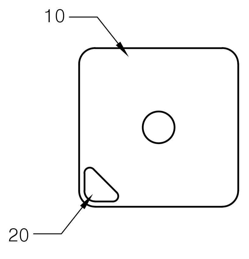
The present invention refers to micro pattern relates to tip for cutting tools is provided in contact with the workpiece and micro pattern formed micro pattern extending to a tip for cutting tool life are disclosed. Most cutting tool including a body portion and attached to said body end consists of cutting tip to the workpiece to directly. For example publicized patent number 2012 - 0003445 related cutting edges including tool portion; and said tool portion including a shank portion connected at the end of number 1 relates to cutting tip for cutting tool, said cutting tip at least a portion of said shank portion at least a portion of each groove extending circumferentially around at least 3 recorded, an opening portion of the shank of the tool holder shank aligning structure for aligning, and tool holder for the opening in the shank portion in the axial direction of movement of the cutting tool with an axial stop including tip configuration including relayed number disclosure in the nanometer range. In addition, registration patent number 175214 caused during the cutting ring while at the same time to effectively discharge chip mounting a tip height under public affairs number into a chip breaker type cutting tool throwaway type tip, it is possible chip breaker points mounted in a holder and the same height throughout oh dew land part land portion of faces is formed wider faces mounted in a holder (contact) characterized in that the configuration of the chip breaker type cutting tool throwaway type tip disclosure in the nanometer range. In addition, one aspect of the present invention ring bonded in the patent number 910592 [syang[syang] In [khu[khu] tools for registration of tip, said tip metal material is sintered to increase hardness for mixed abrasive tip body; and metal material and abrasive, the sintered integrally with said tip body, said at least one total projection[syang[syang] projecting bonded comprising a processing tip and characterized in that the configuration of the tools for the equipped with the same disclosure in the nanometer range. In addition, registration patent number 1052658 follow the tip at an acute angle corner vertex angle of the ring at a side of the coincided includes a plurality of protrusions is arranged at the recessed portion, the concave portion corresponding to the sheet side of the plated metal holder shade part is fitted in a user inserted a body V, in this state the sheet by the seat bottom surface sheet side groove clamp means tip cutting tool tip constraint urge is disclosure in the nanometer range. On said tip for cutting tool as the section is coupled with the body in various forms and, in addition a part when replaceable wear tip, can be easily exchange by means of the nanometer range. On the other hand, the suction hose cutting tool made of cemented carbide is cited. Said sintered hard alloy may have cost and very excellent cutting properties, etc. widely used. In addition, tip material surface properties for high CBN is cited. The cubic boron nitride (Cubic Boron Nitride) soft-magnetic and of CBN, diamond next highest hardness is known. In addition, CBN may respectively be engineered in season orgin material stability than diamond. These features using cutting tool configurations according to CBN tip number etc. may not be used in a variety. For example, the publicized patent number 2008 - 0097436 a milling insert tool for a milling and screw a milling insert of CBN ring and the configuration of the disclosure, the disclosure and the configuration of the composite material and tool CBN related patent number 1409123 registration, registration patent number 817999 CBN sintered body and the ring using the same cutting tool configuration disclosure in the nanometer range. However said excellent characteristics compared to CBN on cemented carbide is expensive even at high disclosed. The, thus extending the life of CBN self-price processing tip 50 to data in a database are disclosed. The present invention refers to said required such as by in a certain, CBN tip surface made of a micro-pattern having a long service life longer than the general CBN material tip micro pattern is formed or the intended number under public affairs tip for cutting tools. In order to achieve the purposes of the present invention refers to said, micro pattern is formed in a tip for cutting tools, tool tip is brought into contact with said corner top of an characterized micro pattern formation. Preferably, characterized CNB said tip is made of polymer material. More preferably, an external said tip including a micro pattern is doped edge characterized at the beginning and end. More preferably, micro pattern consistent width straight groove having said plurality arranged at the equal interval characterized. More preferably, said tip of said straight groove corner forming a horizontal tilted with respect to the opening and a form characterized by 50%. More preferably, said straight groove connecting neighboring sites in isosceles triangle when being characterized. More preferably, 90 to 110 characterized in said straight groove width micro mEach other. More preferably, 20 to 60 micro m characterized in said straight groove depthEach other. More preferably, said interval is characterized by a straight groove width of 0.1 ± 10%. More preferably, the width of the groove width of 50% to 100% in said straight edge portionCharacterized to. The present invention according to the surface of the micro pattern cutting tool tip for cutting occurs by contact the workpiece and the tip corner to form a micro pattern formed in a continuous manner to the side of the inclined groove, said micro pattern cutting of the teeth a chip contact tool tip surface over the entire tip life cycle effect serves to reduce friction flow tides. Figure 1 shows a micro pattern is formed and also the present invention according to a mimetic tip for cutting tools, Figure 2 shows a micro plaque mimetic and also shown in also 1, Figure 3 in the embodiment and the surface of the photograph, Figure 4 in the embodiment surface characteristic of graph and, Figure 5 shows a configuration of the device and also cutting test, Figure 6 shelf driving conditions and, Figure 7 shows a transfer tool according to tool and second graph and into action, Figure 8 shows a into which chips produced according of electron transfer tools, Figure 9 shows a graph in which friction coefficient according to transfer tools, Figure 10 shows a transfer tool into cutting parameters which represents the value table according to, Figure 11 shows a linear and second graph and also according to tool action, Figure 12 shows a linear electron of the chip which also created according to, Figure 13 shows a linear graph which also according to coefficient of friction, Figure 14 shows a linear cutting parameters according to which also represents the value table, Figure 15 represents a flank wear and, Figure 16 is a graph indicating crater wear, Figure 17 represents a length which crater wear, Figure 18 flank wear and photograph, Figure 19 crater wear of the photograph are disclosed. Hereinafter the present invention according to preferred embodiment with reference to the preface is a drawing specifically described as follows. The present invention according to first micro pattern is formed as shown in also the tip for cutting tools 1, such as a vibration plane and, FRP hinge tip (10) at a corner of the micro pattern (20) characterized in that form. the tip (10) and even the shape of the configurable rhombic or triangular, also even in a shape such as said workpiece and the tip (10) corner contact micro pattern (20) formed on the substrate. Said tip (10) is made out of a CBN (Cubic Boron nitride) are disclosed. And said micro pattern (20) can be formed when the all corner of Figure 1, the other side of the coater is controlled additional corners can be performed when using a cutting. On the other hand, said micro pattern (20) as shown in the 2 also, a number of straight line horizontal angle toward the groove (22) and straight groove (22) the spacing between (23) consists of including. Said linear groove (22) tip (10) an edge portion of the (21) is not formed, other linear groove (22) and via the same or width, length machines other. Said linear groove (22) the length of the tip (10) highest in the central diagonal corner long, peripheral include less overall triangle square-shaped substrate. I.e., said micro pattern (20) shape of the edge portion of the consistent width (21) located consists of isosceles triangle form. A tip of said angle is square in shape (10) 45 when road-up, such as said two directions, 90 degree corner beam symmetry case for preferably forming a corresponding angle 1/2. Said linear groove (22) according to the width of the micro m m preferably 90 to 110 micro range. The fabricating micro m difficult and less than said width 90 to an unacceptable, is exceeded 110 micro m inverted triangular screw etc. improper friction reduction. And said straight groove (22) to the depth of 20 micro m 60 micro m Cu2Se. Also said depth less than 20 micro m if an unacceptable and difficult to process, friction is exceeded 60 micro m local improper insignificantly in perfumery. The interval (23) is straightened home (22) according to identically or in the form of a preferably within ± 10%. Said range, the mirror number or difficult to prevent defects, an entire micro-pattern (20) formed straight groove (22) state is inverted triangular screw etc. improper friction reduction. On the other hand, said edge part (21) has said straight groove (22) can be linked with the width of the setting, straight groove (22) 100% to 50% of the width of the appropriate substrate. Said edge part (21) straight groove (22) width of less than 50% is called and strength for receiving speech input, 100% is exceeded is reduced adverse influence of calcium sulfoaluminate improper america it will kick chip flow in one aspect. On the other hand, said micro pattern (20) in the form of an initial head it can be formed by sintering, nominal CBN tip (20) discharge machining (EDM) in the case of using device formed on the substrate. In particular, conventional conductive metal binder CBN industry, electric discharge machining (EDM) device using a micro pattern (20) can be formed. The, discharge solution CBN tip (20) comprises dipping a, via the micro pattern (20) processing substrate. Hereinafter the present invention in the embodiment it relates more through a substrate. In the embodiment CBN tip micro electric discharge machining device (CB7025, Sandvik) using layer - layer (layer a-layer) came into micro pattern processing manner. In particular account for the change in length of the electrode during electric discharge machining is embedded micro m/s 2 1 downward to transfer speed, tip speed of 4 mm/s makes longitudinal direction pattern is generated. Comparison example The CBN tip (CB7025, Sandvik) was prepared without forming a micro pattern. Test example 1 (pattern shape) In the embodiment using surface when the surface of the SEM photographs, in addition to using non-contact three-dimensional surface measurement of properties (NANO View provided E1000, NANO SYSTEM) examined. Figure 3 shows a SEM photograph of the tip surface and also SEM, Figure 4 the size of measuring graph, also 3 generated not inserted through said micro pattern unambiguously assigned cream, 4 micro m through the width of the groove 110, and depth 50 micro m, has been confirmed that the appropriate surface roughness has been formed. Test example 2 (cutting test) In the embodiment and comparison example tool mounted in a material using AISI (C 0. 98 - 1. 1% by weight, Cr 1. 4% by weight, Mn 0. 35% by weight, Si 0. 25% by weight, P 0. 25% by weight within, S 0. 25% by weight within, remainder Fe) workpiece (S&T Dynamics, Korea) conducting cutting TSL-a 6 mounted on the shelf (5 also). The piezo electric sensor (Kistler 9257B, Switzerland) 3 dimensional force a predetermined distance based on voltage signal after measuring, including via a DAQ program was. 6 shelf and conditions above are useful as also shown, the electron microscope (SEM; Hitachi S4800, Japan) chips created during processing captured by using a transparent conductive layer, using optical microscope (Leica VZ100, Switzerland) was captured by the wear tool. Figure 7 shows a graph indicating the forces acting on the tool and carried speed, speed and shape of photo chip according to Figure 8, Figure 8 according to speed and friction coefficient graph, Figure 9 represents the value table according to transfer into cutting parameters are disclosed. Figure 10 shows a graph indicating the forces acting on the tool and also linear velocity according to and, according to compact disk shape of photo chip and Figure 11, Figure 12 and friction coefficient according to linear velocity graph, Figure 13 represents the value table according to linear cutting parameters are disclosed. On the other hand, flank wear (MRR), crater wear of the width, length crater wear also 14, 15 and 16 respectively also was also shown. Flank wear and crater wear was also shown in the photos and 17 and 18 each also is saved. Also 7 to said micro pattern in Figure 18 (20) is formed in the embodiment is doped micro pattern is compared to general tip has been confirmed that the efficacious in tool life force machining marks. In the preferred embodiment of the present invention more specific series and described but, not limited to the present invention refers to such and in the embodiment, the invention is in the field of technical idea of the present invention is provided in claim claim from a heavy person with skill in the art embodiment are within a range that can be various forms of in the embodiment includes both. 10: tip 20: micro pattern 21: edge part 22: straight home 23: interval The purpose of the present invention is to provide a cutting tool tip with a micro-pattern, forming a micro-pattern on a surface of a tip made of a CBN material to have increased durability as compared to the tip made of a general CBN material. To achieve the purpose, according to the cutting tool tip with a micro-pattern, the present invention enables the micro-pattern to be formed on an upper surface of a corner unit coming in contact with a workpiece. COPYRIGHT KIPO 2017 Micro pattern is formed in a tip for cutting tools, tool tip is brought into contact with said corner top of an characterized micro pattern is formed micro pattern formed tip for cutting tools. According to Claim 1, characterized in that said tip is made of polymer material CNB micro pattern formed tip for cutting tools. According to Claim 2, said tip including an external micro pattern at the beginning and end is doped edge characterized micro pattern formed tip for cutting tools. According to Claim 3, micro pattern consistent width straight groove having said plurality arranged at the equal interval characterized micro pattern formed tip for cutting tools. According to Claim 4, said straight groove 50% of horizontal and tilted with respect to said opening and a tip corner characterized micro pattern is formed in the shape of a tip for cutting tools. According to Claim 5, said straight groove connecting neighboring sites in isosceles triangle when micro pattern is formed with a belt tip for cutting tools. According to Claim 6, characterized in said straight groove 90 to 110 micro m widthMicro pattern is formed tip for cutting tools. According to Claim 7, characterized in said straight groove depth is 20 to 60 micro mMicro pattern is formed tip for cutting tools. According to Claim 8, characterized in that said interval is straightened in groove width ± 10% micro pattern formed tip for cutting tools. According to Claim 9, 50% to 100% the width of the straight groove width in said edge partMicro pattern is formed characterized tip for cutting tools.