SEMICONDUCTOR DEVICE, SEMICONDUCTOR CHIP, AND MANUFACTURING METHOD OF SEMICONDUCTOR DEVICE
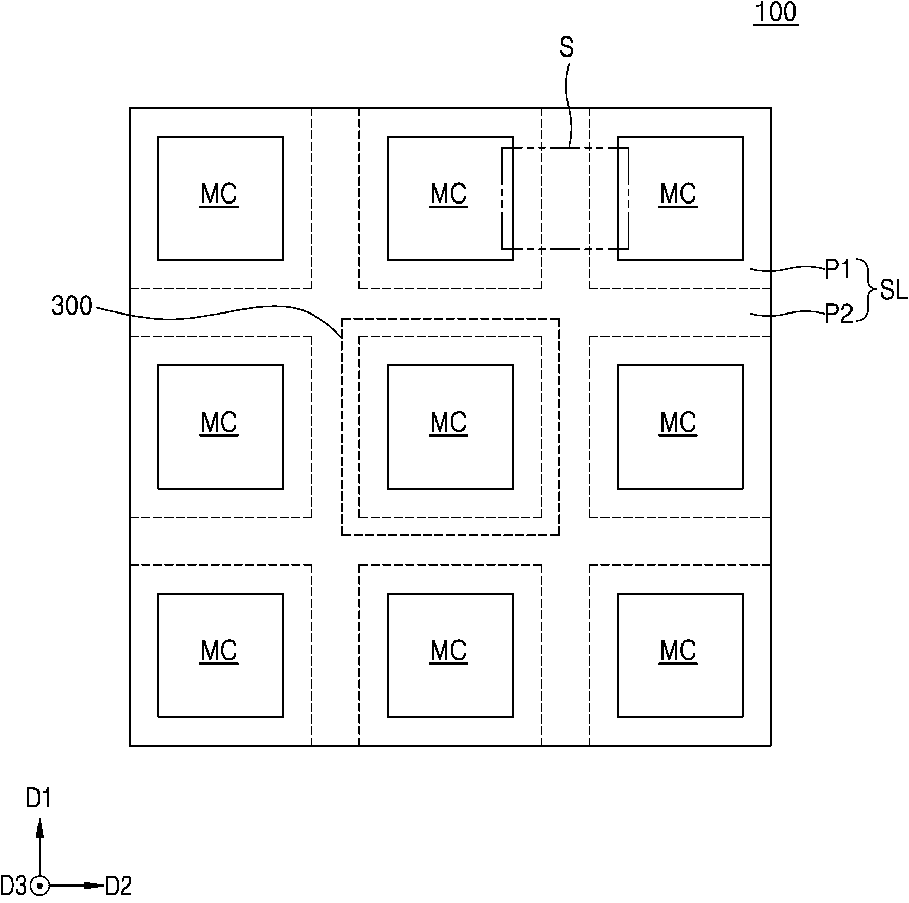
The technical idea of the present invention device, semiconductor chip, and semiconductor device to number of bath method are disclosed. Generally a semiconductor chip includes a semiconductor wafer having integrated circuit die cow five [ing made in the cutting process is performed. During die cow five [ing, cow five [ing blade by cutting the semiconductor wafer along the scribe lane area, as a result a plurality of semiconductor chips are physically apart from each other. Integrated circuit device by the imaging and high integration is required, and can be reduced impurity scribe lane area in a semiconductor wafer, during semiconductor device die cow five [ing applied to integrated I etc. risk due to increased. The technical idea of the present invention comprises a die cow five [ing stress generated during the refining process and number if the integrated circuit semiconductor device from being transferred to a block number [...] 30 to 60 seconds. If the technical idea of the present invention other and a cylinder number of the chip [...] number is 30 to 60 seconds. If the technical idea of the present invention another and number die cow five [ing stress generated during the refining process of the integrated circuit block of a semiconductor device from being transferred to a number number [...] bath method are disclosed. In order to solve the above-described idea is to and a number of the present invention, composed of a main chip region surrounding said which includes a scribe lane, the scribe lane area surrounding said sidewalls of said semiconductor substrate including said number 1 and number 2 number 1 surrounding region, said insulating film on the semiconductor substrate, said insulating film formed on said number 1 in the region of, composed of a number 1 arranged along an edge of said embossing pattern embossing structures including number 1, in the region of said insulating film formed on said number 2, composed of a number 2 arranged along an edge of said embossing pattern embossing structures including number 2, and in the region of said insulating film being formed in the number 1, said insulating layer extending orthogonally with said embossing structure said number 1 in the direction of the dam structures including a semiconductor device insulating layer number [...] substrate. In the embodiment of in technical idea of the present invention, said number 1 extending along the edge of said embossing structure is composed of a length, said length extending along an edge of said number 2 embossing structure is composed of a characterized than longer than that. In the embodiment of in technical idea of the present invention, said number 1 extending along an edge of said embossing structure is composed of a shaped bar (bar), said number 2 (dot) embossing structure characterized as having a dot shape. In the embodiment of in technical idea of the present invention, said dam structure extending along an edge of said sidewalls of said number 1 number 1 embossing structure is composed of a length corresponding to the length extending along an edge of said characterized. In the embodiment of in technical idea of the present invention, said main chip regions number 1 embossing structures composed of a neighboring perpendicularly spaced apart along an edge of said offset being characterized. In the embodiment of in technical idea of the present invention, the patterns of embossing said sidewalls of said number 1 surrounds the edge of the discontinuous characterized. In the embodiment of in technical idea of the present invention, said number 1 exposed between said embossing pattern between said insulating layer and said number 2 of the exposed portion of the insulating said embossing pattern formed on an upper walls of the trench are formed is characterized. In the embodiment of in technical idea of the present invention, said unit has a narrower trench has a form which, in the form of a characterized as having a rounded end. In the embodiment of in technical idea of the present invention, said dam structures extending said upper surface and said insulating film formed on an upper, equal to the number of said number 1 with embossing structure characterized connection. In the embodiment of in technical idea of the present invention, said dam structure, multilayer dummy layers disposed within said insulating layer, said dummy layers connecting the dummy via hole number 1, said dummy layers applied dummy wiring layer connecting said number 1 and number 2 embossing structure bottom, and said insulating layer upper surface, said dummy layers including a lower metal line characterized by a dummy wiring layer connected to the semiconductor element. In the embodiment of in technical idea of the present invention, said dam structure extending up to a point where said said insulating film formed on an upper and lower spaced apart characterized. In the embodiment of in technical idea of the present invention, a portion of which said number 1 and an edge of said embossing structure composed of a main chip along said at the adjacent parts of the interlayer to form characterized as having a shape. In the embodiment of in technical idea of the present invention, said number 2 embossing structures, said number 2 arranged at the center of said number 2 number [...] regions characterized. In the embodiment of in technical idea of the present invention, formed on said insulating layer, and a passivation layer covering at least part of the embossing pattern embossing pattern further including said number 1 characterized said number 2. In the embodiment of in technical idea of the present invention, with said insulating layer in said dam structure disposed between said sidewalls, said sidewalls formed in a continuous manner along an edge of the guard ring structure further comprises. In addition, a number of the present invention and in order to solve the above-described idea is to scribe lane region composed of a semiconductor substrate having a main chip and said residual surrounding regions, said insulating film on the semiconductor substrate, said residual scribe lane region, said insulating layer disposed on the embossing structures including embossing pattern, and in the region of said insulating film in said residual scribe lane, at least a portion of said embossing structure a dam structure and at least in the direction of said insulating layer, said exposed portion of the insulating trench is formed between said embossing pattern is characterized in that a semiconductor chip number [...] substrate. In the embodiment of in technical idea of the present invention, said patterns of embossing, main chip regions surrounding at least a portion of said embossing pattern embossed pattern surrounding said number 1 and number 1 embossing structures including number 1 and number 2 embossing structures embossed pattern including number 2, said dam structures being disposed on the lower side of said number 1 embossing structure characterized. In the embodiment of in technical idea of the present invention, said number 1 extending along the edge of said embossing structure is composed of a line shaped, said dam structure by said number 1 embossing structure is composed of a length extending along an edge of said sidewalls extending along an edge of said characterized. In the embodiment of in technical idea of the present invention, said dam structures, said upper and lower insulating film extending said number 1 and an embossed upper and lower dam structures and said distance from said insulating film to the number of the connected number 1 number 2 dam structure extending spaced points where, said number 1 dam structures disposed adjacent to the than said number 2 dam structures composed of a characterized. In the embodiment of in technical idea of the present invention, formed on said insulating layer, said at least part of the embossing pattern additionally includes a passivation layer, said trenches embossing pattern not covered by said insulating film exposed by said plaque hour hemp cloth [syen in layer characterized portion from the object. Further, a technical idea of the present invention in order to solve the above-described number and said main chip region which includes a scribe lane surrounding edges of sidewalls, said sidewalls of said scribe lane region surrounding said number 1 number 1 and number 2 including the steps of providing a semiconductor substrate region surrounding the, said number 1 in the region of the insulating layer disposed on said semiconductor substrate and an insulation dam structures forming said extending in the direction, and wherein said embossed pattern on forming, said step of forming the embossed pattern, formed on said insulating layer in the region of said number 1, arranged along an edge of said sidewalls corresponding to the embossing structures including number 1 and number 1, in the region of said insulating film formed on said number 2, embossed pattern surrounding said number 1 number 2 embossing structure to form a semiconductor device characterized in that the embossed pattern including number 2 including a number of bath method number [...] substrate. In the embodiment of in technical idea of the present invention, the step of forming the embossed pattern said number 1, said dam structure in the thickness direction so as to be aligned with said insulating said number 1 they are embossed to form embossed pattern said number 1 characterized. In the embodiment of in technical idea of the present invention, corresponding to the after, said embossed pattern etching mask, said insulating film of the isolation layer portion further including a stand-alone number characterized. In the embodiment of in technical idea of the present invention, the step of forming said trench, said embossing pattern including forming a passivation layer on at least a portion of said covering, said first passivation mask layer exposing an upper portion, and said embossed pattern with said mask layer and etching mask, said exposed portion including a number of insulating layer and underlying passivation layer characterized by a stand-alone. In the embodiment of in technical idea of the present invention, the step of forming the embossed pattern said number 1 they are composed of a bar-shaped extending along an edge of said embossing said number 1 is formed with a and, the step of forming the embossed pattern said number 2 dot shapes a flat embossing said number 2 they are characterized. In the embodiment of in technical idea of the present invention, the step of forming the embossed pattern said number 1, said it sees an embossed number 1 main chip regions composed of a neighboring perpendicularly spaced apart along an edge of said offset so that they are characterized. In the embodiment of in technical idea of the present invention, the step of forming the embossed pattern said number 2, they are embossing said number 2 number of said number 2 arranged at said number 2 to center said number 2 [...] regions characterized embossed pattern form. Technical idea of the present invention is a semiconductor device die cow five [ing cracks generated during the refining process and clear the scribe lane area composed of a pattern of embossments and/or dams can be intercepting includes the structure. The, cracks and clear the scribe lane area during die cow five [ing main chip formation region in the injection hole can prevent integrated circuit, semiconductor device is separated and in addition can be improve the reliability of semiconductor chip prepared by the number. In the embodiment of the present invention are according to semiconductor device by technical idea is also 1a to 1c also to account for a drawing as, technical idea of the present invention in the embodiment according to the semiconductor device 1a is also one of coarse plane view and, 1a 1b "S" also includes a first region of a semiconductor device also contains display of coarse plane view and, also 1b 1c is also of A - A ' line according to the schematic diagram of the semiconductor device and wire cross-sectional drawing are disclosed. Also 2a and 2b also comprises a die cow five [ing noninsulin cracks generated within the scribe lane area during the process to determine the aspect represented by the drawing are disclosed. Figure 4 shows a technical idea of the present invention also 3 and also one in the embodiment according to drawing to explain the dam structure as, 3 and Figure 4 also 1b also each of A - A ' line of coarse vertical section according to semiconductor device are disclosed. Figure 5 shows a semiconductor device in the embodiment according to technical idea of the present invention also one of embossed pattern number 1 to explain the plane are disclosed. Figure 6 shows a semiconductor device in the embodiment according to technical idea of the present invention also one of embossed pattern number 1 to explain the plane are disclosed. Figure 7 shows a semiconductor device in the embodiment according to technical idea of the present invention also of number 2 of the vertical section of are disclosed. Figure 8 shows a semiconductor device in the embodiment according to technical idea of the present invention also one of embossed pattern number 2 to explain the plane are disclosed. Figure 9 shows a semiconductor device in the embodiment according to technical idea of the present invention also of dam structure a portion represented by the sensors mounted thereon to determine number 1 embossing structure are disclosed. Figure 10 shows a semiconductor device in the embodiment according to the embossing patterns of and insulating film formed on top of the technical idea of the present invention also of indicating cross trench are disclosed. In the embodiment of the present invention are according to semiconductor device by 11a and 11b also is also technical idea as to account for a drawing, technical idea of the present invention is also one in the embodiment according to the semiconductor device 11a of coarse plane view and, also 11a 11b also is of B - B ' according to the schematic diagram of the semiconductor device and wire cross-sectional drawing line are disclosed. In the embodiment of the present invention are according to semiconductor device by 12a and 12b also is also technical idea as to account for a drawing, technical idea of the present invention is also one in the embodiment according to the semiconductor device 12a of coarse plane view and, also 12a 12b is also of C - C 'ray and D - D' line according to the schematic diagram of the semiconductor device and wire cross-sectional drawing are disclosed. In the embodiment of the present invention are according to semiconductor device also includes a number of technical idea of also 13a to 13f bath method shown in order to explain the process to cross-sectional drawing are disclosed. In the embodiment of the present invention are semiconductor device according to number of technical idea is also 14a and 14b also describe a method of bath cross-sectional drawing are disclosed. Figure 15 shows a cross-section of the technical idea of the present invention also by one in the embodiment according to semiconductor package 2000 Hereinafter, in the embodiment of the present invention with reference to the attached drawing a specific detailed the on-sensors other. In the present invention to the art person with skill in the art of the present invention in the embodiment are more completely describe a target ball number and, in the embodiment is to various other shape can be, in the embodiment of the present invention limited to a range not the. The complete disclosure and such further fidelity rather these in the embodiment, of the present invention to one skilled in the event number for which to more fully convey the ball are disclosed. In addition, drawing descriptive convenience and clarity in the thickness or size of each layer for S. and apparatus. Throughout the specification, one component of other components "on", or "connected" when referred to that position, the aforementioned one component with other components directly "on", "connected" in contact with or, sheets can be interpreted that another components may be present. While, one component of other components "directly on", or "directly connected" mentioned that when located, there may be another component sheets is not interpreted substrate. The same code is identical elements defines other. As used in the specification, the term "and/or" all listed in item corresponding one and at least one combination. In the specification number 1, number 2 of various terms in the member, component, region, layers and/or partial but used to explain, these members, components, regions, layers and/or partial must not be defined by these terms by a nontrivial disclosed. These term one element, component, region, layer or a part of the other areas, are used for distinguishing or partial layer formed on. The, above-mentioned hereinafter the number 1 member, component, region, layer or portion of the present invention without leaving the present number 2 member, component, region, layer or a part of the can be defines. In addition, "on" or "over" and "under" or "beneath" relative terms such as illustration in the drawing as if they were other factors for any elements can be use therein describes a relationship. In addition to the drawing direction described in relative terms of including other directions can be understand that intended to be. For example, if a component of in one drawing can be inverted (turned over), other factors present on a face of the top of the above other elements of the lower portion of the elements that a straight line direction on the surface to be coated. Therefore, the term "on" fields for example, particular orientation dependent "under" and "on" direction of the drawings can be both. (Other direction with respect to the 90 degree rotation) if components directed in different directions, the specification can be used in land the relative interpreted. The terms used in particular are used in specification to account for in the embodiment, the present invention relayed a number for endured. As used in the specification, if not a single shape providing language translators in other cases identified deficiencies in a more precise manner, can be a plurality of types. In addition, when used in the specification and/or "including (comprising)" "comprises (comprise)" handle shapes, number, step, operation, member, element and/or presence of these particular in which, one or more diverse shapes, number, operation, member, element and/or the presence or addition times number groups does not disclosed. Hereinafter, in the embodiment of the present invention in the embodiment of the present invention are ideal as shown in reference to determine the drawing through a browser substrate. Drawing substrate in, for example, techniques and/or tolerances according number bath (tolerance), can be shown in shape deforming are expected. Thus, in the embodiment of the present invention is shown in the event it became grudge not interpreted in the region specification number and shape, for example number larger than the size variation of the resulting should contain other. Hereinafter in the embodiment are a combination of one or several may be filled in the base station. In addition, the term "substrate" used in the specification substrate itself, or substrate and the like formed on the surface layer or film can be laminated structure including predetermined means. Semiconductor device and semiconductor chip is configuration described hereinafter may have here the needed only illustratively being in number, the present invention is not limited to content found each other. In the embodiment of the present invention is technical idea according to semiconductor device are also 1a to 1c also by (100) as to account for a drawing, technical idea of the present invention is also 1a by one in the embodiment according to semiconductor device (100) of coarse plane view and, 1a 1b "S" also includes a first region of a semiconductor device also contains display (100) plane view and of coarse, also 1b 1c is also of A - A ' line in accordance with the semiconductor device (100) and wire cross-sectional drawing schematic diagram of are disclosed. Also 1a to 1c also reference the, semiconductor device (100) is composed of a main chip area (MC) and said (MC) (SL) between the scribe lane area formed in the substrate (102), said semiconductor substrate (102) on insulating film (104), said scribe lane area (SL) in said insulating film (104) embossing pattern disposed on (120), and said scribe lane area (SL) in said insulating film (104) disposed within the dam structure (110) can be include. Wherein, semiconductor device (100) includes a plurality of IC devices are including be a semiconductor wafer. Said semiconductor substrate (102) can be a semiconductor material, e.g., silicon (Si, silicon) can be comprising. Or, said semiconductor substrate (102) is that [me (Ge, germanium) such as semiconductor elements, or SiC (silicon carbide), GaAs (gallium arsenide), InAs (indium arsenide), and InP (indium phosphide) compound semiconductor material such as can be. In another example, semiconductor substrate (102) SOI (semiconductor on insulator) such as the silicon on insulator structure may have. Semiconductor substrate (102) is conductive region, for example impurity doped well (well), or impurities can be doped structure. Said insulating layer (104) is said semiconductor substrate (102) can be disposed on one side of. Said insulating film (104) includes a plurality of interlayer dielectric (104) can be are being extended. Said insulating layer (104) of silicon, silicon nitride, or it can be mxsiyo2, not the limited to said illustrative bar. As also shown in 1a, semiconductor device (100) is composed of a (MC) and a scribe lane area (SL) can be. Semiconductor device (100) includes a plurality of sidewalls comprising (MC) can be, sidewalls of the scribe lane area neighboring (MC) and an outer (SL) can be spaced disclosed. The semiconductor device is composed of a (MC) can be. Said device is or can be logic elements. In addition, various kinds of a plurality of equipment for processing said semiconductor device can be. A plurality of discrete element said various microelectronic device, for example, CMOS transistor such as MOSFET, system LSI (large scale integration), such as Image sensor (CMOS imaging sensor) CIS, MEMS, active, passive element can be like. Said scribe lane area (SL) can be disposed between neighboring sidewalls (MC), (MC) can be composed of a surrounding. Scribe lane area (SL) during die cow five [ing (die sawing) process can be cutting by cow five [ing blade (2a also BL of reference). The scribe lane area (SL) (MC) and said sidewalls of said sidewalls of said at the adjacent parts of said number 1 (P1) (P1) (MC) edge of the number 1 and number 2 region surrounding the region surrounding region comprising (P2) can be. I.e., number 1 (P1) (P2) is composed of a number 2 region and an outer region (MC) and can be spaced disclosed. Wherein, number 1 region (P1) during die cow five [ing may be passed by a closure comprising a cow five [ing blade (BL), number 2 (P2) during die cow five [ing (BL) region passes can be truncated portion is cow five [ing blade. I.e., the number 2 (P2) semiconductor device along cow five [ing blade (BL) region (100) can be cutting. Said cow five [ing die by said semiconductor substrate (102) and said semiconductor substrate (102) to prevent cutting film or the like formed on a variety of materials, said semiconductor device (100) includes a plurality of semiconductor chip (300) can be separated into. On the other hand, in of the present invention in the embodiment, semiconductor chip (300) and said main chip area (MC) (MC) composed of a scribe lane area comprising peripheral remaining (reference of Figure 15 RSL) can be. Wherein, residual scribe lane are formed through device (100) for performing (MC) composed of a cow five [ing die after peripheral means (SL) can be left in the scribe lane area. For example, number 1 (P1) said number 1 (P1) and said residual scribe lane region is region that is adjacent the region can be a portion of region number 2 (P2). As also shown in 1c, said embossing pattern (120) the scribe lane area (SL) in insulating film (104) can be disposed on. Said embossing pattern (120) insulating film (104) has an embossing structure projecting from the upper surface of the dry etch chamber (122, 124) can be composed. Embossing structure (122, 124) are e.g. aluminum, or aluminum alloy but, limited to are not correct. Embossing pattern (120) between the insulating layer to expose selectively (104) at least one trench (125) can be formed. In the embodiment in part, said trench (125) is said to embossed pattern first etch mask, said insulating film (104) number can be formed by a portion of a stand-alone. Said trench (125) has embossing structure (122, 124) from the bottom of lower-level extending to depth may have. In the embodiment in part, said embossing pattern (120) is disposed number 1 number 1 region (P1) embossing structure (122) embossing pattern consisting of number 1 (121) and number 2 region (P2) embossing structure disposed number 2 (124) embossing pattern consisting of number 2 (123) can be comprising. Said dam structure (110) are said scribe lane area (SL) in said insulating film (104) can be disposed within. Dam structure (110) are said insulating film (104) starting from the lower surface, said insulating layer (104) extending in the thickness direction (e.g., number 3 (D3) direction) can be. Further, said dam structure (110) are composed of a discontinuous edge of the surrounding or partially surrounding said (MC) can be. Said embossing structure (122, 124) and at least a portion of said insulating layer (104) in the thickness direction (e.g., number 3 (D3) direction) can be aligned to. E.g., said dam structure (110) are can be conductive material. 2A and 2b also comprises a die cow five [ing also during scribe lane area (SL) generated within the crack (CR) to determine noninsulin aspect represented by the drawing are disclosed. Also 1a, 2a and 2b also reference the also, cow five [ing blade (BL) is an insulating film (104) in a direction toward the lower surface from the upper surface of insulating film (104) and semiconductor substrate (102) is equal to cutting. Cow five [ing blade (BL) (SL) semiconductor device along the scribe lane area (100) during cutting, cow five [ing blade (BL) on insulating layer (104) between physical friction by the axial stress is performed with each other. This stress in a semiconductor device (100) and clear the cause cracking (CR) in all, crack (CR) the main chip area (MC) is equal to the clear into the integrated circuit. As also shown in 2a, cow five [ing blade (BL) is an insulating film (104) extending downward from the top of the semiconductor device where it is cutting, embossing pattern (BL) is cow five [ing blade (120) is equal to contact with. The, embossing pattern (120) around the crack initiated at the embossing pattern (CR) (120) and the insulating layer (104) moves along an interface switches the trench (125) while stress are dispersed crack (CR) can be driving transistor see, or trench (125) noninsulin direction of depth of the crack (CR) (MC) without cracking (CR) the main chip area and clear the semiconductor substrate (102) is equal to upper ends of the proceeds. As also shown in 2b, cow five [ing blade (BL) on insulating film (104) or the semiconductor substrate (102) is composed of a portion in contact with the clear (MC) originates at the dam structure toward cracking (CR) (110) are encountered on. Said dam structure (110) includes a crack (CR) (MC) toward the main chip area can interrupt the tremor. The 1c also again referencing, dam structure (110) are said insulating film (104) from the lower surface of the insulating film (104) extending the upper surface of the can. Said dam structure (110) are said insulating film (104) in the thickness direction (e.g., direction number 3 (D3)) and aligned, insulating film (104) exposed at the top of the embossing pattern (120) can be connected to a part of. In an exemplary in the embodiment, said dam structure (110) are said insulating film (104) arranged in multilayer dummy layer number 1 at a height level other dummy interconnection layer (113a) and number 2 dummy interconnection layer (113b), said multilayer dummy wiring layer connecting the dummy via number 1 (115a), said multilayer dummy layers is applied number 2 dummy interconnection layer (113b) and said number 1 embossing structure (122) connecting the dummy via number 2 (115b), and insulating film (104) extends out from the lower surface of said lowermost dummy interconnection layer multilayer dummy layers said number 1 (113a) connected to the dummy via contact (111) can be comprising. In addition, but not shown in the drawing, dam structure (110) is lower metal contact (111) connected to upper ends of, said dummy via contact (111) may have a support pattern. In the embodiment in part, said support pattern is formed (102) can be ball number but embedded form. Not limited to the semiconductor substrate (102) projecting from one side of the form number ball 1308. It can be said support pattern is e.g. poly silicon, said limited to the configuration of the support pattern are not correct. On the other hand, the dam structure also 1c (110) including a dummy wiring layer is layer 2 of example but when, technical idea of the present invention and are not limited to, dam structure (110) layers is more than layer 2 can be, e.g. 4 layer, or 8 layer dummy wires can be layers. Or said dam structure (110) includes a single dummy wires can be layer. Figure 4 shows a technical idea of the present invention also 3 and also one in the embodiment according to drawing to explain the dam structure as, 3 and Figure 4 also 1b also each of A - A ' line of coarse vertical section according to semiconductor device are disclosed. The reference also 3, dam structure (110a) is said insulating film (104) extending from the lower surface of, said insulating film (104) can be spaced a predetermined distance from the upper surface of 2000. Thus, dam structure (110a) are embossed pattern (120) can be separated from. For example, dam structure (110a) is also shown in 3 such as said insulating film (104) extending vertically from the lower surface of the upper metal line (111) can be unit so as. But, dam structure (110a) which are not limited to the configuration of the, dam structure (110a) also includes rings as shown in 3, 1 also shown in dummy interconnection layer number 1 (113a), dummy via number 1 (115a), and number 2 wiring layer (213b) further comprise at least one of the disapproval. The reference also 4, dam structure (110b) are said insulating film (104) extending from the lower surface of the upper number 1 dam structure (110 _ 1) and said insulating layer (104) extending from the lower surface of said insulating film (104) from the upper surface of which a number 2 dam structure (110 _ 2) can be made. Said number 1 dam structure (110 _ 1) have at least a portion of the embossing pattern (120) while connected, said number 2 dam structure (110) are embossed pattern (120) can be away from. In the embodiment in part, said number 1 dam structure (110 _ 1) are said number 2 dam structure (110 _ 2) (MC) can be disposed adjacent to the drain region disclosed are disposed. Again, the reference also 1a to 1c, said embossing pattern (120) includes a plurality of number 1 embossing structure (122) embossing pattern having number 1 (121) and a plurality of number 2 embossing structure (124) embossing pattern having number 2 (123) can be comprising. Embossing pattern number 1 (121) of the scribe lane area (SL) number 1 region (P1) can be disposed within, (MC) can be at least partly surrounding edges of the sidewalls. In addition, embossing pattern number 2 (123) region of the scribe lane area (SL) number 2 (P2) can be disposed within, embossing pattern number 1 (121) may surround disclosed. In other words the, embossing pattern number 2 (123) embossing pattern the number 1 (121) and an outer (MC) and sidewalls can be spaced disclosed. In the embodiment in part, embossing pattern number 1 (121) number 1 constituting the embossing structure (122) embossing pattern on number 2 (123) number 2 constituting the embossing structure (124) to each may have other shapes. E.g., number 1 embossing structure (122) a length extending along an edge of the main chip area (MC) (e.g., number 1 embossing structure (122) is number 1 direction (D1) extending length) is number 2 embossing structure (124) a length extending along an edge of the main chip area (MC) (e.g., number 2 embossing structure (124) extending length direction (D1) is number 1) longer than can be configured. Embossing pattern number 1 (121) number 1 constituting the embossing structure (122) is composed of a (MC) or main line shape extending along an edge of the direction (MC) edge of the drain region sides bar (bar) may have shape. Embossing pattern number 2 (123) number 2 constituting the embossing structure (124) includes a dot (dot) may have shape. In addition, in the embodiment in part, number 1 embossing structure (122) and/or number 2 embossing structure (124) has its side may have. In other words the, said number 1 embossing structure (122) and/or number 2 embossing structure (124) are interlinked narrowed direction may have a shape. On the other hand, line-shaped or bar-shaped extending along the edge of (MC) composed of a number of number 1 embossing structure (122) are disposed in parallel each other along edges of the sidewalls (MC) and widthwise lamp, surrounding (MC) can be discontinuous to the main chip area. In addition, a plurality of number 1 said embossing structure (122) are composed of a (MC) direction away from edges of the main chip area (MC) arranged multilayer can be arranged in a surrounding a pair. Dot shape (dot) number of number 2 embossing structure (124) are disposed along an edge of sidewalls (MC) and, at the same time away from said drain region (MC) can be disposed in parallel. For example, a plurality of number 2 embossing structure (124) are matrix (matrix) can be arranged in. Figure 5 shows a semiconductor device in the embodiment according to technical idea of the present invention also of embossing pattern of number 1 (121) to a planar to explain are disclosed. With reference also to the 1a also 5, a plurality of number 1 embossing structure (122) are composed of a direction along the edge of (MC) (e.g., number 1 direction (D1)) which are arranged in layers, in addition direction perpendicular to one of the sidewalls (MC) (e.g., number 2 (D2) direction) can be arranged. Said number 1 direction (D1) a transponder number 1 embossing structure (122) are said number 1 (D1) direction of discharge spaced, said number 2 direction (D2) a transponder number 1 embossing structure (122) are said number 2 (D2) direction of discharge can be spaced disclosed. Said number 1 embossing structure (122) are composed of a multilayer surrounds (MC), surrounding or partially surrounding the edge of the drain region (MC) can be discontinuous. On the other hand, one of the sidewalls (MC) (e.g., number 2 (D2) direction) direction perpendicular to a transponder number 1 embossing structure (122) are composed of a direction along the edge of (MC) (e.g., number 1 direction (D1)) interval (x1) number 1 along offset can be arranged. As a result, number 1 embossing structure (122) direction (D2) can be arranged for example in the form is realized while said number 2. Said number 1 (D1) (D2) 3 disposed in a widthwise direction of discharge offset direction of said number 2 number 1 embossing structure (122) formed when that one group, number 1 embossing structure (122) form a number 1 direction (D1) are a plurality of said number 2 and can be arranged in a direction (D2). For example, number 1 and number 2 (G1) (G2) group of number 1 embossing structures which are arranged in the direction said number 2 (D2) group of number 1 embossing structures, number 3 and number 4 group of number 1 (G3) (G4) group of number 1 embossing structures said number 2 (D2) can be arranged in the direction embossing structures. In addition, group of number 1 number 1 (G1) and number 3 (G3) embossing structures which are arranged in the direction (D1) group of number 1 embossing structures said number 1, number 2 number 1 and number 4 (G4) embossing structures (G2) group of the group number 1 (D1) said number 1 direction embossing structures can be arranged. Here, number 1 of 3 embossing structure (122) while said number 1 (D1) are shown but one group formed in an offset direction, forming one group number 1 embossing structure (122) limited to the number of blocks are not correct. Figure 6 shows a semiconductor device in the embodiment according to technical idea of the present invention also of embossing pattern of number 1 (121a) describe a planar are disclosed. With reference also to the 1a also 6, embossing pattern number 1 (121) and an edge at the adjacent parts of the main chip area (MC), composed of a double-sided embossing structure (MC) along the edge of the form number 1 (122b) can be include. Number 1 in the form bent said embossing structure (122b) are composed of a (MC) which is connected to the whole edges must be not, only some of the edge of the drain region (MC) can be. Figure 7 shows a semiconductor device in the embodiment according to technical idea of the present invention also of number 2 of the vertical section of are disclosed. The reference also 7, number 2 embossing structure (124) are said number 2 (P2) said number 2 (P2) for the edge portions of a center region (P2 _c) number [...] region (P2 _e) can be arranged. Wherein, number 2 (P2) region (P1) and (P2) for the edge portions is number 2 (P2 _e) number 1 number 2 (P2) during boundary region region region adjacent regions can be means. I.e., number 2 (P2) for the edge portions of both sides of the center region (P2 _c) number 2 (P2) is equal to (P2 _e) region on contact. Die cow five [ing at a cow five [ing blade during a blade area (BL) directly by means which may be truncated portion, in the embodiment of the present invention said number 2 (P2) and the center of said portion in said number 2 (P2) blade area region (P2 _c) region (P2 _c) (P2) (P2 _e) center of adjacent edge portions of said number 2 region can be a portion. In other words the, number 2 (P2 _c) (P2) (BL_w) width of blade area can be greater than the width of the center area. Thus, die during said number 2 (P2) cow five [ing at a center of (P2 _c) cow five [ing blade (BL) region is along the semiconductor device (100) where it is cutting, the both side portions of a cow five [ing blade (BL) number 2 embossing structure (124) and rests on, cow five [ing blade center portion is number 2 (BL) embossing structure (124) without contact with the insulating film (104) can be directly cutting. (P2) number 2 (BL) cow five [ing blade contact center of number 2 (P2 _c) embossing structure is primarily region (124) is arranged not to, number 2 embossing structure (124) is formed to the generation of particles broken JPO. Figure 8 shows a semiconductor device in the embodiment according to technical idea of the present invention also of number 2 of embossing pattern (123a) to a planar to explain are disclosed. The reference also 8, embossing pattern number 2 (123) number 2 constituting the embossing structure (124) includes a dot (dot) may have shape. The, number 2 embossing structure (124) are also 1b can be differently as the scan. I.e., number 2 embossing structure (124) are number 1 can be arranged in a zigzag along direction (D1). Or, number 2 embossing structure (124) are along the scan direction number 2 (D2) can be. Figure 9 shows a semiconductor device in the embodiment according to technical idea of the present invention also of dam structure (110) and a portion of the embossing structure number 1 (122) represented by the sensors mounted thereon to determine are disclosed. Also 1a 1c and also to the reference 9 also, dam structure (110) number 2 region (P2) are disposed, said number 1 embossing structure (122) and said insulating layer (104) can be aligned in the thickness direction. In some in the embodiment, number 1 embossing structure (122) extending along the edge of the main chip area (MC) has line-shaped or bar-shaped, said number 1 embossing structure (122) disposed on the lower side of dam structure (110) is said number 1 embossing structure (122) in the same manner as on line shape extending along an edge of the main chip area (MC) or a bar shape may have. The, said dam structure (110) is composed of a number 1 (MC) along an edge of length (L1) can be extended by, said dam structure (110) has a length (L1) of number 1 number 1 embossing structure (122) is corresponding to the length extending along an edge of said sidewalls (MC) can be. Figure 10 shows a semiconductor device in the embodiment according to technical idea of the present invention also of the embossing patterns of and insulating film (104) formed on top of the trench (125) indicating cross-section are disclosed. The reference also 1c are symmetrically 10, number 1 embossing structure (122) or number 2 embossing structure (124) are insulating film (104) disposed on the, neighboring number 1 embossing structure (122) embossing structure between or number 2 (124) in between the trench (125) can be formed. In some in the embodiment, trench (125) is an insulating film (104) from the upper surface of lower direction can be formed by a given depth, trench (125) may have itself and narrower at the bottom, end of rounded form may have. Said rounded in the form trench (125) cracking is more uniformly dispersed into a plurality of stages, crack more effectively number can be a stand-alone. On the other hand, edge of said sidewalls (MC) (e.g., number 2 (D2) direction) direction perpendicular to, number 1 embossing structure (122) or number 2 embossing structure (124) are number 1 may have a width (w1), neighboring number 1 embossing structure (122) embossing structure between or number 2 (124) the width between the number 2 can be spaced disclosed. Wherein, said number 1 width (w1) number 1 the embossing structure (122) or number 2 embossing structure (124) can be bottom of means in width. The width said number 2 (w2) said number 1 embossing structure (122) or number 2 embossing structure (124) of the same height level neighboring lessen the number 1 embossing structure (122) between neighboring interval or number 2 embossing structure (124) can be distance between the means. In the embodiment in part, can be greater than the width (w2) said number 1 width (w1) said number 2. For example, the width about 2 times said number 1 width (w1) said number 2 (w2) implementation being. On the other hand, when referring also to also 1a 1c again, in the embodiment in part, said embossing pattern (120) between the insulating layer to expose selectively (104) to a portion of the number of special trench (125) is formed extending in an overall communication can be. Or, in other in the embodiment, said trench (125) is an insulating film (104) can be formed only in a specific region of. In the embodiment of the present invention are according to semiconductor device by 11a and 11b also is also technical idea (100c) as to account for a drawing, technical idea of the present invention is also 11a by one in the embodiment according to semiconductor device (100c) of coarse plane view and, 11a 11b also is also of B - B ' line in accordance with the semiconductor device (100c) and wire cross-sectional drawing schematic diagram of are disclosed. Also 11a and 11b also shown in semiconductor device (100c) is guard ring structure forming region (GR) and guard ring structure forming region disposed guard ring structure (GR) (130) shown in fig. 1a to 1c and also that a number [...] and to semiconductor device (100) may have substantially the same as those configuration. Also 11a and 11b also in, also 1a to 1c identical reference number can also exhibit a same member, here described character recognition for the dispensed or simply as follows. The 11a and 11b also also reference, number 1 (P1) and (P2) the scribe lane area (SL) can be region number 2 region comprising, said number 1 (P1) region is formed as the structure (130) that is provided with a guard ring structure forming region comprising (GR) can be. Said guard ring structure forming region (GR) (MC) can be surrounding the edge of the main chip area. Said guard ring structure (130) includes a dam structure (110) and sidewalls (MC) can be disposed between. Said guard ring structure (130) is composed of a (MC) can be continuously along an edge of the shape of a surrounding, ring-shaped or loops may have shape. In also 11b, said guard ring structure (130) surrounds the edge of the (MC) is composed of a double-shown but, guard ring structure (130) limited to the number of are not correct. Said guard ring structure (130) includes an insulating film (104) can be disposed within. Said guard ring structure (130) includes an insulating film (104) starting from the lower surface, said insulating layer (104) extending in the thickness direction can be. In the embodiment in part, said guard ring structure (130) is formed in an guard ring structure forming region (GR) embossing pattern is (120) disposed may not disclosed. Or, in other in the embodiment, said guard ring structure forming region (GR) embossing pattern is number 1 (121) can be formed, number 1 embossing structure (122) includes a guard ring structure (130) on the insulating film (104) can be aligned in the thickness direction. The, said guard ring structure forming region disposed number 1 (GR) embossing structure (122) is said guard ring structure (130) in the same manner as on or formed in a continuous manner along an edge of the main chip area (MC), or said guard ring structure (130) to the other can be the exposure. On the other hand, in the embodiment in part, said guard ring structure (130) includes said insulating film (104) from the lower surface of the insulating film (104) extending the upper surface of the can. Said guard ring structure (130) also 1c is shown in dam structure (110) can be on substantially the same configuration. I.e., said guard ring structure (130) is lower metal contact, dummy layers and bottom can be made. But, guard ring structure (130) which are not limited to the configuration of the, 1c also shown in dam structure (110) can be configured to a transformational hereinafter. In other in the embodiment, guard ring structure (130) includes said insulating film (104) extending from the lower surface of, said insulating film (104) can be spaced a predetermined distance from the upper surface of 2000. Said guard ring structure (130) 3 is also shown in dam structure (110) such as, can be comprised of upper metal line. But, guard ring structure (130) limited to the configuration of the are not correct. In the embodiment of the present invention are according to semiconductor device by technical idea is also 12a and 12b also (100c) as to account for a drawing, technical idea of the present invention is also one in the embodiment according to the semiconductor device 12a (100c) of coarse plane view and, also 12a 12b is also of C - C 'ray and D - D' line in accordance with the semiconductor device (100c) and wire cross-sectional drawing schematic diagram of are disclosed. Also 12a and 12b also shown in semiconductor device (100c) is passivation layer (140) shown in fig. 1a to 1c and also that a number further comprises [...] semiconductor device (100) may have substantially the same as those configuration. Also 12a and 12b also in, also 1a to 1c identical reference number can also exhibit a same member, here described character recognition for the dispensed or simply as follows. The reference also 12a and 12b also, semiconductor device (100) includes an insulating film (104) formed on, embossing pattern (120) covering at least some of passivation layer (140) can be further. In the embodiment in part, said passivation layer (140) is said insulating film (104) that is can comprises different materials. E.g., said passivation layer (140) can be composed of silicon nitride layer. In some in the embodiment, passivation layer (140) can be formed only in a portion of the scribe lane area (SL). Thus, passivation layer (140) is embossing pattern (120) and covering a portion of, the embossing patterns (120) can be another aspect of partially exposed. The, said insulating film (104) on passivation layer (140) portion is formed trench (125) is formed there can be, against the insulating film (104) on passivation layer (140) are linked to each other trench is doped (125) can be formed. In the embodiment of the present invention are according to semiconductor device also includes a number of technical idea of also 13a to 13f bath method shown in order to explain the process to cross-sectional drawing are disclosed. Also shown in semiconductor device 13a to 13f also 1a to 1c also also in (100) for example to explain number bath method of for example less than 1000. Also 13a to 13f also-sound device (100) of scribe lane area (SL) exhibits drain region and (MC) together. The reference also 13a, scribe lane area (SL) having sidewalls (MC) semiconductor substrate (102) to 4700. Then, the semiconductor substrate scribe lane area (SL) (102) on one side of dummy via contact (111) is formed, said semiconductor substrate (102) on one side of dummy via contact (111) number 1 peripheral filling interlayer dielectric (104a) formed on the substrate. In addition, (MC) composed of the semiconductor substrate (102) on one side of via contact (211) and forming at least one transistor (TR), said semiconductor substrate (102) on one side of via contact (211) and transistor (TR) number 1 that surrounds said interlayer insulation film (104a) formed on the substrate. In some in the embodiment, but not shown in the drawing, upper metal line (111) and via contact (211) each having at its one side can be formed on the support. Said support pattern is, for example, semiconductor substrate (102) can be ball number but embedded form. Not limited to the semiconductor substrate (102) projecting from one side of the form number ball 1308. It can be said support pattern is e.g. poly silicon, said limited to the configuration of the support pattern are not correct. Said number 1 interlayer dielectric (104a) of silicon, silicon nitride, or silicon can be mxsiyo2. Said transistor (TR) includes a substrate (102) is formed on one side of the gate electrode structure, said gate electrode structure located on both sides said semiconductor substrate (102) can be formed by doping impurities therein. In addition, in the embodiment in part, disposed in the scribe lane area (SL) said dummy via contact (111) and disposed in said drain region (MC) via contact (211) metal, metal silicide, impurity doped semiconductor, or a combination of them can be made. For example, dummy via said contact (111) and said via contact (211) tungsten, nickel, cobalt, tantalum primary drum such as metal, tungsten silicide, nickel silicide, cobalt silicide, tantalum silicide metal silicide such as a primary drum, impurity doped polysilicon, or a combination thereof but may include, said limited to the illustrated bar and not the. Then, across said number 1 (MC) and composed of a scribe lane area (SL) interlayer insulation film (104a) number 2 on interlayer insulation film (104b) formed on the substrate. Said number 2 interlayer dielectric (104b) (SL) the scribe lane area disposed within the dummy interconnection layer number 1 (113a) and include, (MC) composed of a wiring layer disposed in the number 1 (213a) can be comprising. Said number 1 dummy interconnection layer (113a) is said dummy via contact (111) can be connected, said number 1 wiring layer (213a) is said via contact (211) can be connected. Said number 2 interlayer dielectric (104b) of silicon, silicon nitride, or silicon can be mxsiyo2. In the embodiment in part, said number 1 dummy interconnection layer (113a) and number 1 wiring layer (213a) to form, said number 1 interlayer dielectric (104a), dummy via contact (111), and via contact (211) number 2 covering the interlayer insulation film (104b) formed on a substrate, said number 2 interlayer dielectric (104b) some stand-alone number to number 2 interlayer dielectric (104b) through said upper metal line (111) and via contact (211) can be arranged in a plurality of line-shaped exposing. Then, damascene process using a plurality of line shape of openings that dummy interconnection layer filling said number 1 (113a) and number 1 wiring layer (213a) scribe lane area (SL) each composed of a (MC) can be formed. The reference also 13b, number 2 interlayer dielectric (104b) number 3 on interlayer insulation film (104c), number 4 interlayer dielectric (104d) and number 5 interlayer dielectric (104e) is laminated in sequence. Number 3 interlayer dielectric (104c) (SL) the scribe lane area number 1 in dummy via (115a) and include, drain region (MC) number 1 in via (215a) can be a. Number 4 interlayer dielectric (104d) the scribe lane area (SL) in dummy interconnection layer number 2 (113b) and include, (MC) composed of a number 2 in wiring layer (213b) can be comprising. Number 5 interlayer dielectric (104e) (SL) the scribe lane area number 2 in dummy via (115b) and include, (MC) composed of a number 2 in via (215b) can be a. More specifically, composed of a scribe lane area (SL) (MC) and number 2 over the interlayer insulating film (104b) number 3 on interlayer insulation film (104c) formed on the substrate. Number 3 interlayer dielectric (104c) number 1 in dummy interconnection layer (113a) and number 1 wiring layer (213a) formed exposing openings, conductive material filled with dummy via number 1 said openings (115a) on number 1 via (215a) can be formed. Then, number 3 (SL) (MC) and composed of a scribe lane area over the interlayer insulating film (104c) number 4 on interlayer insulation film (104d) formed on the substrate. Then, using a damascene process, dummy interconnection layer number 2 (113b) and number 2 wiring layer (213b) can be formed. Next, composed of a scribe lane area (SL) number 4 (MC) and over an interlayer insulating film (104d) number 5 on interlayer insulation film (104e) formed on the substrate. Number 5 interlayer dielectric (104e) number 2 in dummy interconnection layer (113b) and number 2 wiring layer (213b) formed exposing openings, said conductive material filled with dummy via number 2 openings (115b) on number 2 via (215b) can be formed. Said number 3 interlayer dielectric (104c) to said number 5 interlayer dielectric (104e) silicon, silicon nitride, or silicon can be mxsiyo2. In the embodiment in part, said dam structure (110) constituting said upper metal line (111), dummy interconnection layer number 1 (113a), dummy via number 1 (115a), dummy interconnection layer number 2 (113b), and number 2 dummy via (115b) is composed of a line-shaped or bar-shaped extending along the edge of (MC) can be made to have 13C also reference surface, said insulating layer (104) metal layer on a (120L) formed on the substrate. Said metal layer (120L) sidewalls of the scribe lane area (SL) (MC) can be formed on both. For example, said metal layer (120L) is aluminum or aluminum alloy but, and not limited to the illustrated said. The reference also 13d, said metal layer (120L) by patterning, scribe lane area (SL) in embossing pattern (120) is formed, composed of (MC) in landing pad (220) can be formed. In the embodiment in part, also 13d also consults with a 1b when, said embossing pattern (120) is formed embossing pattern number 1 (P1) number 1 region (121) and number 2 region (P2) embossing pattern formed number 2 (123) can be formed to include. Number 1 embossing structure (122) and dam structure (110) are said insulating film (104) can be overlap in the thickness direction of a position. In the embodiment in part, embossing pattern number 1 (121) number 1 to at least two embossing structure (122) embossing pattern and number 2 (123) number 2 at least two embossing structure (124) having different geometries may be patterned to each other. For example, number 1 embossing structure (122) and number 2 embossing structure (124) are composed of a length extending along an edge of said hereinafter (MC) can be formed on each other. Or, number 1 embossing structure (122) are composed of a line-shaped or bar-shaped extending along the edge of (MC) can be made to have, number 2 embossing structure (124) are dot shapes can be formed to have. The reference also 13e, embossing pattern (120) at the fifth step to said embossing pattern (120) between the insulating layer to expose selectively (104) a portion of a stand-alone number trench (125) can be formed. Said trench (125) is said trench (125) is said embossing pattern (120) extends from the bottom of lower-level can be formed. On the other hand, 13e also in said trench (125) number 4 is an interlayer insulating film (104d) as shown but the upper surface of the groove is formed, which is an exemplary said trench (125) can be tightly controlled depth of various. The reference also 13f, die cow five [ing process is performed, semiconductor substrate (102) and semiconductor substrate (102) various material layer formed on cow five [ing blade (BL) by cutting with each other. As a result, semiconductor device includes a plurality of semiconductor chip can be separated into. Said semiconductor chip and said main chip area (MC) composed of (MC) (SL) can be remaining around a scribe lane area. On the other hand, in the scribe lane area (SL) (MC) 13a to 13f also also composed of a number of minimizing shown consists of a process for preparing together but, to other scribe lane area (SL) (MC) is composed of a number of minimizing process for preparing can be separately made. Or more, also 13a to 13f also refers to the semiconductor device (100) number of bath method is described but, also within the range of technical idea of the present invention just described 13a to 13f also refers to various deformation and minor modifications from various semiconductor device (100) can be form. In the embodiment of the present invention are semiconductor device according to number of technical idea is also 14a and 14b also describe a method of bath cross-sectional drawing are disclosed. Also 14a and 14b also composed of a scribe lane area (SL) of-sound device exhibits (MC) together. The reference also 14a, 13a to 13d also makes rough semiconductor device also substantially on (100) is ready. Then, said insulating film (104) said on embossing pattern (120) and landing pad (220) covering the passivation layer (140) is formed, said passivation layer (140) on said passivation layer (140) to expose portions of the mask layer (150) formed on the substrate. Said mask layer (150) is embossing pattern (120) of forming a second passivation layer (140) expose, landing pad (220) formed on a passivation layer (140) can be exposing a portion of. Said passivation layer (140) is said insulating film (104) that is can comprises different materials. E.g., said passivation layer (140) can be composed of silicon nitride layer. The 14b also reference, said mask layer (150) and said embossing pattern (120) together hole exposes a mask layer (150) between the exposed passivation layer (140) and underlying insulating film (104) as an etch mask can be disclosed. In scribe lane area (SL), said mask layer (150) and said embossing pattern (120) is used as together, insulating film (104) trench is formed by etching a portion of the (125) and form. In sidewalls (MC), mask layer (150) between the exposed passivation layer (140) the number of special points, said landing pad (220) exposing the pad window (140w) can be formed. Then, mask layer (150) is of special number can be disclosed. On the other hand, also shown in semiconductor device also 12a and 12b (100) the following steps are performed in the embodiment can be in some form. Said insulating film (104) on passivation layer (140) is formed, said passivation layer (140) on said passivation layer (140) to expose portions of the mask layer formed on the substrate. The, said embossing pattern mask layer (120) can be formed only in at least a portion of the upper. Then, said mask layer etching mask is performed process has a plurality of hierarchies. Said etching a result of the process, mask layer exposed between the passivation layer (140) and underlying insulating film (104) number trench while a portion of the wetting ability (125) is formed, mask layer covered by a passivation layer (140) and underlying insulating film (104) thereof can is selectively etched. Then, the mask layer number 1308. wetting ability. In the embodiment of the present invention are more technical idea according to semiconductor device by an exemplary number bath method example described but for example, within the range of technical idea of the present invention just described from said various modifications and minor modifications, the semiconductor device of the present invention example 12b also 1a from within the range of technical idea also to various semiconductor device structures are various modified change is applied to the engine-case number high pressure liquid coolant to one skilled will. Figure 15 shows a technical idea of the present invention also by one in the embodiment according to semiconductor package (1000) cross-section of the disclosed. The reference also 15, semiconductor package (1000) includes a package substrate (1100), package substrate (1100) in the side to semiconductor chips (1200), connecting member (1300), molding member (1400), and external connection member (1500) can be a. Said semiconductor chip (1200) to the semiconductor device through the die for cow five [ing 14b also 1a also described by using the number bath 1308. Said package substrate (1100) is an upper wiring layer (1110), bottom wire layer (1120), and said upper wiring layer (1110) and bottom wire layer (1120) connecting the internal wiring (1130) can be comprising. Said upper wiring layer (1110) interconnecting member (1300) chip pad through (1210) connected to the previous gate, said bottom wire layer (1120) to an external connection member (1500) can be connected. Such, an upper wiring layer (1110), bottom wire layer (1120) and internal wiring (1130) interconnecting member (1300) and external connection member (1500) package substrate with (1100) that is mounted on a semiconductor chip (1200) mediator electrically connecting the external device can function. Said semiconductor chip (1200) comprising sidewalls of the central portion thereof and the semiconductor element can be formed, can be remaining periphery thereof comprising scribe lane area (RSL). Wherein, integrated circuit elements formed on semiconductor device with respect to the scribe lane area (RSL) residual cow five [ing die out after remaining around means can be composed of a scribe lane area. Said residual scribe lane area (RSL) prevent a main chip area for dam structure and/or noninsulin cracks can be embossing pattern. Semiconductor chip (1200) to a package board (1100) can be in the side to, package substrate (1100) and a semiconductor chip (1200) disposed between a connection member (1300) can be electrically connected by. In some in the embodiment, semiconductor chip (1200) memory element, logic element (e.g., a microprocessor, analog device, digital signal processor (digital signal processor)), or system - on - chip (System On Chip) performing various be a semiconductor chip. Said memory device for example, dram (DRAM), SRAM (SRAM), flash (flash) memory, EEPROM (EEPROM), [...] (PRAM), MRAM (MRAM), or the like can be the ram which will know (RRAM). In addition semiconductor chip (1200) includes at least two or more semiconductor chips are laminated structure (multi-a chip) a multi - chip may be disclosed. For example, at least two or more semiconductor chips may all have the same kinds of memory element, two or more semiconductor chip and one of the memory element, the other microcontroller (Micro-a controller) can be an element disclosed. Connection member (1300) includes a top wiring layer (1110) is formed on, semiconductor chip (1200) confronts (1100) performing the function of electrically connecting the can. Connection member (1300) is improved in a shielding material, copper (Cu), aluminum (Al), solder (solder), is (Ag), tin (Sn), gold (Au) can be like. For example connection member (1300) is solder balls (solder ball), solder bump (solder bump), formed by the metal filler (pillar) and solder made bumps or wire bonding device be a wire. On the other hand, in the embodiment in part, semiconductor chip (1200) is not trench is remaining scribe lane area (RSL) can be, the connection member (1300) includes a semiconductor chip (1200) (RSL) remaining scribe lane area can be located under the dummy connection member (1300a) can be a. But, in the embodiment in other, said dummy connection member (1300a) may be omitted is disapproval. Molding member (1400) has a package substrate (1100) on semiconductor chip (1200) can be formed to encircle. Molding member (1400) is epoxy (epoxy-a group) molding resin or polyimide-based (polyimide-a group) can be like molding resin. The semiconductor chip of the present invention in the embodiment according to (1200) in main chip scribe lane area during die cow five [ing eliminated by preventing cracks developing noninsulin, prevent said second active region can be adjusted by integrated circuit. Further, semiconductor chip (1200) residual stress (RSL) dam structure and/or embossing pattern so that the scribe lane area, semiconductor package (1000) of the semiconductor chip assembly process (1200) which can be applied to main due to integrated circuit within the chip-forming regions can prevent damage. All of the technical idea of the present invention description is to avoid a described illustratively provided, in the present invention if the properties of the present invention is provided to essentially inputted from deviating from a person with skill in the art various modifications and deformable will. Thus, the present invention in the embodiment of the present invention are to define the disclosure but rather to explain the technical idea and, in the embodiment of the present invention by not the limited range of such feature. Under the protection range of the present invention must be interpreted by fee so as to range, its equivalent range of all technical idea is within the range of the present invention will be interpreted rights. 100: Semiconductor device 102: Semiconductor substrate 104: Insulating film 110: Dam structure 120: Embossing pattern 121: Embossing pattern number 1 122: Number 1 embossing structure 123: Embossing pattern number 2 124: Number 2 embossing structure 125: Trench 130: Guard ring structure 140: Passivation layer 300: Semiconductor chip MC: composed of SL: scribe lane area P1: number 1 region P2: number 2 region The present invention provides a semiconductor device, comprising: a semiconductor substrate including a main chip region and a scribe lane region surrounding the main chip region, wherein the scribe lane region includes a first region surrounding the main chip region and a second region surrounding the first region; an insulating film on the semiconductor substrate; a first embossing pattern formed on the insulating film in the first region, and including first embossing structures arranged along an edge of the main chip region; a second embossing pattern formed on the insulating film in the second region, and including second embossing structures arranged along the edge of the main chip region; and dam structures formed in the insulating film in the first region, extending in the thickness direction of the insulating film, and aligned with the first embossing structures in the thickness direction of the insulating film. COPYRIGHT KIPO 2017 Drain region surrounding said main chip region which includes a scribe lane, the scribe lane area surrounding said sidewalls of said semiconductor substrate including said number 1 number 1 and number 2 region surrounding; said insulating film on the semiconductor substrate; in the region of said insulating film formed on said number 1, composed of a number 1 arranged along an edge of said embossing pattern embossing structures including number 1; in the region of said insulating film formed on said number 2, composed of a number 2 embossing structures including number 2 arranged along an edge of said embossing pattern; and said number 1 being formed in the in the region of said insulating layer, said insulating layer extending orthogonally with said insulating layer in the direction of the dam structures including said number 1 embossing structure semiconductor device. According to Claim 1, said number 1 extending along the edge of said embossing structure is composed of a length, said length extending along an edge of said number 2 embossing structure is composed of a semiconductor device characterized in that the longer than. According to Claim 1, said number 1 extending along an edge of said embossing structure is composed of a shaped bar (bar), said number 2 embossing structure characterized as having a dot shape (dot) device. According to Claim 3, said dam structure extending along an edge of said sidewalls of said number 1 number 1 length length extending along an edge of said embossing structure is composed of a corresponding semiconductor device characterized. According to Claim 3, said embossing structures said number 1 main chip regions neighboring perpendicularly offset a predetermined distance from the drain region along an edge of semiconductor device characterized. According to Claim 1, said number 1 the patterns of embossing said discontinuously surrounds the semiconductor device composed of a edge of the characterized. According to Claim 1, said number 1 exposed between said embossing pattern between said insulating layer and said number 2 of the exposed portion of the insulating said embossing pattern is formed on an upper walls of the trench is formed in a semiconductor device characterized. According to Claim 7, said unit has a narrower trench has a form which, characterized as having a round end supplied with the device. According to Claim 1, said dam structures extending said upper surface and said insulating film formed on an upper, an embossed characterized said number 1 to the number of the connection device. According to Claim 9, said dam structure, multilayer dummy layers disposed within said insulating layer, said dummy layers connecting the dummy via hole number 1, said dummy layers applied dummy wiring layer connecting said number 1 and number 2 embossing structure bottom, and said insulating layer upper surface, said dummy layers including dummy wiring layer semiconductor element connected semiconductor device characterized in that the lower metal line. According to Claim 1, said dam structure extending up to a point where said said insulating film formed on an upper and lower spaced apart characterized semiconductor device. According to Claim 1, a portion of which said number 1 and an edge of said embossing structure composed of a main chip shape along said at the adjacent parts of the interlayer to form characterized as having a device. According to Claim 1, said number 2 embossing structures, said number 2 region arranged at center of said number 2 number [...] regions characterized semiconductor device. According to Claim 1, formed on said insulating layer, and a passivation layer covering at least some of said number 1 characterized in that said number 2 embossing pattern embossing pattern further including semiconductor device. According to Claim 1, with said insulating layer in said dam structure disposed between said sidewalls, said sidewalls including semiconductor device formed in a continuous manner along an edge of the guard ring structure. Said main chip region surrounding the scribe lane region semiconductor substrate having a main chip regions remaining; said insulating film on the semiconductor substrate; said residual scribe lane region, said insulating layer disposed on the embossing structures including embossing pattern; and in the region of said insulating film in said residual scribe lane, said embossing structure and said at least some of the insulating layer in the direction of the dam structure and at least a, said exposed portion of the insulating between said embossing pattern is characterized in that the trench is formed in a semiconductor chip. According to Claim 16, said patterns of embossing, main chip regions surrounding at least a portion of said embossing pattern embossed pattern surrounding said number 1 and number 1 embossing structures including number 1 and number 2 embossing structures embossed pattern including number 2, characterized in that said dam structures positioned under said number 1 embossing structure of a semiconductor chip. According to Claim 17, said number 1 extending along the edge of said embossing structure is composed of a line shaped, said dam structure said number 1 said embossing structure is composed of a length extending along an edge of said characterized by sidewalls extending along an edge of a semiconductor chip. Main chip regions surrounding said main chip region which includes a scribe lane, the scribe lane area surrounding said sidewalls of said semiconductor substrate including the steps of providing a region surrounding said number 1 number 1 and number 2; said insulating layer in the region of the insulating film disposed on said semiconductor substrate and said number 1 extending in the direction forming a dam structures; and wherein said embossed pattern on forming, said step of forming the embossed pattern, formed on said insulating layer in the region of said number 1, arranged along an edge of said sidewalls corresponding to the embossing structures including number 1 and number 1, in the region of said insulating film formed on said number 2, embossed pattern surrounding said number 1 number 2 embossing structures including number 2 semiconductor device including forming a number of embossed pattern characterized bath method. According to Claim 19, the step of forming the embossed pattern said number 1, said insulating film in the thickness direction so as to be aligned with said dam structure they are embossing said number 1 corresponding to the number of semiconductor device characterized in that said number 1 bath method.