Semiconductor module
The present invention relates to a semiconductor module. In the related art, a volatile memory (RAM) such as a dynamic random access memory (DRAM) is known as a storage device. DRAMs are required to have high performance of an arithmetic unit (hereinafter referred to as a logic chip) and a large capacity capable of withstanding an increase in amount of data. Therefore, the capacity has been increased by miniaturizing a memory (memory cell array, memory chip) and increasing the number of cells in a plane. On the other hand, this type of increase in capacity has reached its limit due to the weakness to noise caused by the miniaturization, the increase in die area, and the like. Therefore, in recent years, a technology has been developed that realizes a large capacity by laminating a plurality of planar memories to form a three-dimensional (3D) structure. In addition, there has been proposed a semiconductor module that reduces an installation area of the logic chip and the RAM by overlapping the logic chip and RAM (see, for example, Patent Documents 1 to 4).
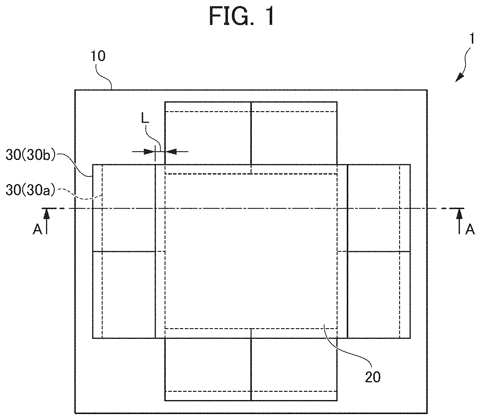
With the increase in performance of the logic chip and the increase in amount of data, an improvement in communication rate between the logic chip and the RAM is also required along with the increase in capacity. Therefore, it is preferable to provide a semiconductor module capable of improving a bandwidth between the logic chip and the RAM. An object of the invention is to provide a semiconductor module capable of improving a bandwidth between a logic chip and a RAM. The invention relates to a semiconductor module including: a logic chip; a pair of RAM units, each of which is configured with a lamination-type RAM module; a first interposer electrically connected to the logic chip and each of the pair of RAM units; and a connection unit that communicatively connects the logic chip and each of the pair of RAM units, in which one RAM unit is placed on the first interposer and has one end portion disposed so as to overlap one end portion of the logic chip with the connection unit therebetween in a lamination direction, and in which the other RAM unit is disposed so as to overlap the one RAM unit with the connection unit therebetween and is disposed along at least one side of the outer periphery of the logic chip. In addition, it is preferable that each of the pair of RAM units include a memory unit in which memory circuits are laminated, and an interface chip laminated on one end side of the memory unit. In addition, it is preferable that each of the pair of RAM units be disposed with the interface chips facing each other. In addition, it is preferable that, in each of the pair of RAM units, the interface chip be disposed on a surface opposite to a surface facing the first interposer. In addition, it is preferable that the other RAM unit be configured to include only the memory unit. In addition, it is preferable that the semiconductor module further include a second interposer placed on the other RAM unit, a third interposer or a package substrate on which the first interposer is placed, and a bonding wire that electrically connects the second interposer and the third interposer or the package substrate. In addition, it is preferable that the semiconductor module further include a second interposer placed on the other RAM unit and a columnar member that electrically connects the first interposer and the second interposer. In addition, it is preferable that the semiconductor module further include a heat sink unit placed on the other RAM unit and the logic chip. In addition, it is preferable that the heat sink unit include a spacer member adjacent to at least one of the other RAM unit and the logic chip. In addition, it is preferable that each of the pair of RAM units include a lamination-type RAM module having the same shape and size in plan view. According to the invention, it is possible to provide a semiconductor module capable of improving a bandwidth between a logic chip and a RAM. Hereinafter, semiconductor modules according to embodiments of the invention will be described with reference to the drawings. The semiconductor module according to each embodiment is, for example, a system in a package (SIP) in which arithmetic units (hereinafter referred to as logic chips) and lamination-type RAMS are disposed on an interposer. The semiconductor module is disposed on a different interposer and is electrically connected by using micro bumps. The semiconductor module is a device that can obtain power from different interposers and can transmit and receive data to and from different interposers. In addition, in each of the following embodiments, an MPU will be described as an example of the logic chip. Next, a semiconductor module 1 according to a first embodiment of the invention will be described with reference to As illustrated in The MPU 20 is a plate-like body having a rectangular shape in plan view. As illustrated in Each of the pair of RAM units 30 is configured to include a lamination-type RAM module having a rectangular shape in plan view. For example, each of the pair of RAM units 30 is configured to include a lamination-type DRAM module. As illustrated in The one of the pair of RAM units 30 (hereinafter referred to as the one RAM unit 30 As illustrated in By disposing a plurality of the other RAM units 30 Each of the pair of RAM units 30 includes a memory unit 31 and an interface chip 32 as illustrated in The memory unit 31 is formed in a plate-like body having a rectangular shape in plan view and is formed by laminating memory circuits 33 The interface chip 32 is formed in a plate-like body having a rectangular shape in plan view. The interface chip 32 is laminated on one end side (upper surface side) of the memory unit 31. Specifically, the interface chip 32 is laminated on the memory circuit 33 The connection unit 40 is a communication interface that connects the MPU 20 and each of the pair of RAM units and is formed in, for example, a layered shape. The connection unit 40 communicatively connects the MPU 20 and the pair of RAM units 30. That is, the MPU 20 and the pair of RAM units 30 are communicatively connected to each other. The connection unit 40 is disposed on the surface (upper surface) opposite to the surface (lower surface) placed on the first interposer 10 among the surfaces of the one RAM unit 30 As illustrated in Next, operations of the semiconductor module 1 will be described. First, as illustrated in In a case where a data is stored in the pair of RAM units 30, first, a data D1 is transmitted from the first interposer 10 to the MPU 20. The MPU 20 transmits a calculation result calculated on the basis of the data D1 to the pair of RAM units 30 as a store signal (data D2). That is, the store signal transmitted from the MPU 20 is transmitted through the circuit surface 21 and the connection unit 40 of the MPU 20 to the interface chip 32 of the one RAM unit 30 The interface chip 32 stores the data included in the store signal in the memory unit 31 on the basis of the address included in the store signal (data D3). At this time, the interface chip 32 also controls the other RAM unit 30 On the other hand, in a case where a data is loaded from the pair of RAM units 30, first, a load signal is transmitted from the first interposer 10 to the MPU 20 (data D6). That is, the load signal transmitted from the MPU 20 is transmitted through the circuit surface 21 and the connection unit 40 of the MPU 20 to the interface chip 32 of the one RAM unit 30 The interface chip 32 loads the data from the corresponding address in the memory unit 31 on the basis of the address included in the load signal (data D5). At this time, the interface chip 32 also controls the other RAM unit 30 The semiconductor module 1 according to the first embodiment as described above has the following effects. (1) The semiconductor module 1 is configured to include the MPU 20 (logic chip), a pair of the RAM units 30 each of which is configured with the lamination-type RAM module, and the first interposer 10 which is electrically connected to the MPU 20 and each of the pair of RAM units 30, and the connection unit 40 which communicatively connects the MPU 20 and each of the pair of RAM units 30. Then, the one end portion of one of the pair of RAM units 30 is disposed so as to overlap the one end portion of the MPU 20 in the lamination direction C with the connection unit 40 therebetween, and the other of the pair of RAM units 30 is disposed so as to overlap the one RAM unit 30 (2) Each of the pair of RAM units 30 is configured to include the memory unit 31 in which the memory circuits 33 (3) In each of the pair of RAM units 30, the interface chip 32 is disposed on the surface side opposite to the surface facing the first interposer 10. Accordingly, since the disposition can be performed without changing the direction of the lamination direction of the RAM units 30, the ease of manufacturing improves. (4) The semiconductor module 1 is further configured to include the heat sink unit 50 placed on the other RAM unit 30 (5) Each of the pair of RAM units 30 is configured to include the lamination-type RAM module having the same shape and size in plan view. Accordingly, since it is not necessary to manufacture the lamination-type RAM module corresponding to each of the pair of RAM units 30 according to individual standards, the manufacturing cost can be reduced. (6) The power W4 and the ground G4 are supplied from the interface chip 32 to the MPU 20 with the connection unit 40 therebetween. Accordingly, a common power can be supplied to the drive circuit that drives the signal line between the interface chip 32 and the MPU 20, and thus, malfunction due to a phase shift of power source noise can be effectively suppressed. Next, a semiconductor module 1A according to a second embodiment of the invention will be described with reference to The semiconductor module 1A according to the second embodiment as described above has the following effects. (7) Each of the pair of RAM units 30 is disposed with the interface chips 32 facing each other. Accordingly, each of the pair of RAM units 30 can be controlled by separate interface chips 32. Next, a semiconductor module 1B according to a third embodiment of the invention will be described with reference to The semiconductor module 1B according to the third embodiment as described above has the following effects. (8) The other RAM unit 30 Next, a semiconductor module 1C according to a fourth embodiment of the invention will be described with reference to The second interposer 60 is formed to have a rectangular shape in plan view. For example, the second interposer 60 is placed on the other RAM unit 30 The bonding wire 70 is disposed so as to supply a power W3 and a ground G3 to the other RAM unit 30 Next, operations of the semiconductor module 1C will be described. As illustrated in The semiconductor module 1C according to the fourth embodiment as described above has the following effects. (9) The semiconductor module 1C is configured to further include the second interposer 60 placed on the other RAM unit 30 Next, a semiconductor module 1D according to a fifth embodiment of the invention will be described with reference to The columnar member 90 is, for example, a Cu pillar and is disposed so as to supply a power W5 and a ground G5 to the other RAM unit 30 Next, operations of the semiconductor module 1D will be described. As illustrated in The semiconductor module 1D according to the fifth embodiment as described above has the following effects. (10) The semiconductor module 1D is configured to further include the second interposer 60 placed on the other RAM unit 30 Next, a semiconductor module according to the sixth embodiment of the invention will be described. In the description of the sixth embodiment, the same components are denoted by the same reference numerals, and the description thereof is omitted or simplified. The semiconductor module according to the sixth embodiment is different from the first to fifth embodiments in that the heat sink unit 50 includes a spacer member (not illustrated). In a case where there is a step difference between the upper surface of the MPU 20 and the upper surface of the other RAM unit 30 The semiconductor module according to the sixth embodiment as described above has the following effects. (11) The heat sink unit is configured to include at least a spacer member adjacent to one of the other RAM unit 30 While the preferred embodiments of the semiconductor module according to the invention have been described above, the invention is not limited to the above-described embodiments and can be modified as appropriate. For example, in the above-described embodiment, the power supply terminal and the ground terminal that connect the laminated dies 33 In addition, in the above-described embodiment, the connection unit 40 is an ACF, but the invention is not limited thereto. For example, the connection unit 40 can be configured as illustrated in Table 2 below. In the fourth embodiment, the heat sink unit 50 may be formed to have a size that does not overlap the connection portion between the bonding wire 70 and the second interposer 60. As another modified example, the heat sink unit 50 may have a spacer member having a height larger than the height of the bonding wire 70 from the second interposer 60 and having a size that does not overlap the connection portion between the bonding wire 70 and the second interposer 60. In the above-described embodiment, the power W1 and the power W2 are supplied from the first interposer 10 to the MPU 20 and the pair of RAM units 30, but the invention is not limited thereto. For example, as illustrated in In addition, the arithmetic unit is not limited to the MPU and may be widely applied to all logic chips. The memory is not limited to the DRAM and may be applied to all random access memories (RAMS) including a wide range of non-volatile RAMS (for example, MRAMs, ReRAMs, FeRAMs, and the like). EXPLANATION OF REFERENCE NUMERALS
The present invention provides a semiconductor module capable of improving a bandwidth between a logic chip and a RAM. According to the present invention, a semiconductor module 1 is provided with: a logic chip; a pair of RAM units 30 each composed of a lamination-type RAM module; a first interposer 10 electrically connected to the logic chip and to each of the pair of RAM units 30; and a connection unit 40 that communicatively connects the logic chip and each of the pair of RAM units 30, wherein one RAM unit 30a is placed on the first interposer 10, and has one end portion disposed so as to overlap, in the lamination direction C, one end portion of the logic chip with the connection unit 40 therebetween, and the other RAM unit 30b is disposed so as to overlap the one RAM unit 30a with the connection unit 40 therebetween, and is also disposed along the outer periphery of the logic chip. 1. A semiconductor module comprising:
a logic chip; a pair of RAM units, each of which is configured with a lamination-type RAM module; a first interposer electrically connected to the logic chip and each of the pair of RAM units; and a connection unit that communicatively connects the logic chip and each of the pair of RAM units, wherein one RAM unit is placed on the first interposer and has one end portion disposed so as to overlap one end portion of the logic chip with the connection unit therebetween in a lamination direction, and the other RAM unit is disposed so as to overlap the one RAM unit with the connection unit therebetween and is disposed along at least one side of an outer periphery of the logic chip. 2. The semiconductor module according to wherein each of the pair of RAM units includes:
a memory unit in which memory circuits are laminated; and an interface chip laminated on one end side of the memory unit. 3. The semiconductor module according to 4. The semiconductor module according to 5. The semiconductor module according to 6. The semiconductor module according to a second interposer placed on the other RAM unit; a third interposer or a package substrate on which the first interposer is placed; and a bonding wire that electrically connects the second interposer and the third interposer or the package substrate. 7. The semiconductor module according to a second interposer placed in the other RAM unit; and a columnar member that electrically connects the first interposer and the second interposer. 8. The semiconductor module according to 9. The semiconductor module according to 10. The semiconductor module according to TECHNICAL FIELD
BACKGROUND ART
DISCLOSURE OF THE INVENTION
Problems to be Solved by the Invention
Means for Solving the Problems
Effects of the Invention
BRIEF DESCRIPTION OF THE DRAWINGS
PREFERRED MODE FOR CARRYING OUT THE INVENTION
First Embodiment
Second Embodiment
Third Embodiment
Fourth Embodiment
Fifth Embodiment
Sixth Embodiment
1 Bumpless TSV TCI 2 Bumpless TSV TSV + Hybrid Bonding 3 Bumpless TSV Bumpless TSV 4 TSV + Hybrid Bonding TCI 5 TSV + Hybrid Bonding TSV + Hybrid Bonding 6 TSV + Hybrid Bonding Bumpless TSV 7 ACF TCI 8 ACF ACF
In addition, TCI is an abbreviation for ThruChip Interface.
1 ACF ACF ACF ACF 2 ACF TCI ACF TCI 3 Hybrid Bonding Hybrid Bonding Hybrid Bonding Hybrid Bonding 4 Hybrid Bonding TCI Hybrid Bonding TCI 5 Micro bump Micro bump Micro bump Micro bump 6 Micro bump TCI Micro bump TCI


CPC - классификация
GG1G11G11CG11C5G11C5/G11C5/0G11C5/02G11C5/025G11C5/06G11C5/063HH0H01H01LH01L2H01L22H01L222H01L2224H01L2224/H01L2224/1H01L2224/13H01L2224/131H01L2224/1314H01L2224/13147H01L2224/16H01L2224/162H01L2224/1622H01L2224/16227H01L2224/3H01L2224/32H01L2224/321H01L2224/3214H01L2224/32145H01L2224/33H01L2224/331H01L2224/3318H01L2224/33181H01L2224/7H01L2224/73H01L2224/732H01L2224/7320H01L2224/73203H01L2224/7325H01L2224/73253H01L2225H01L2225/H01L2225/0H01L2225/06H01L2225/065H01L2225/0651H01L2225/06517H01L2225/0652H01L2225/06524H01L2225/0656H01L2225/06562H01L2225/0658H01L2225/06589H01L23H01L23/H01L23/3H01L23/36H01L23/367H01L23/3672H01L23/4H01L23/49H01L23/498H01L23/4981H01L23/49811H01L23/49816H01L23/5H01L23/53H01L23/538H01L23/5385H01L24H01L24/H01L24/1H01L24/13H01L24/16H01L24/3H01L24/32H01L24/33H01L24/4H01L24/45H01L24/7H01L24/73H01L25H01L25/H01L25/0H01L25/04H01L25/042H01L25/06H01L25/065H01L25/0652H01L25/0655H01L25/0657H01L25/07H01L25/071H01L25/1H01L25/11H01L25/112H01L25/18H01L27H01L27/H01L27/0H01L27/02H01L27/020H01L27/0203H01L29H01L292H01L2924H01L2924/H01L2924/1H01L2924/14H01L2924/143H01L2924/1431H01L2924/1435H01L2924/15H01L2924/153H01L2924/1531H01L2924/15311H01L2924/19H01L2924/191H01L2924/1910H01L2924/19107H1H10H10DH10D8H10D89H10D89/H10D89/0H10D89/00IPC - классификация
HH0H01H01LH01L2H01L23H01L23/H01L23/0H01L23/00H01L23/3H01L23/36H01L23/367H01L23/4H01L23/49H01L23/498H01L25H01L25/H01L25/0H01L25/06H01L25/065H01L25/07H01L25/1H01L25/11H01L27H01L27/H01L27/0H01L27/02Цитирование НПИ
257/686257/686
257/737
257/773
361/679.55