MULTI-FUNCTION TERMINAL OF POWER SUPPLY CONTROLLER FOR FEEDBACK SIGNAL INPUT AND OVER-TEMPERATURE PROTECTION
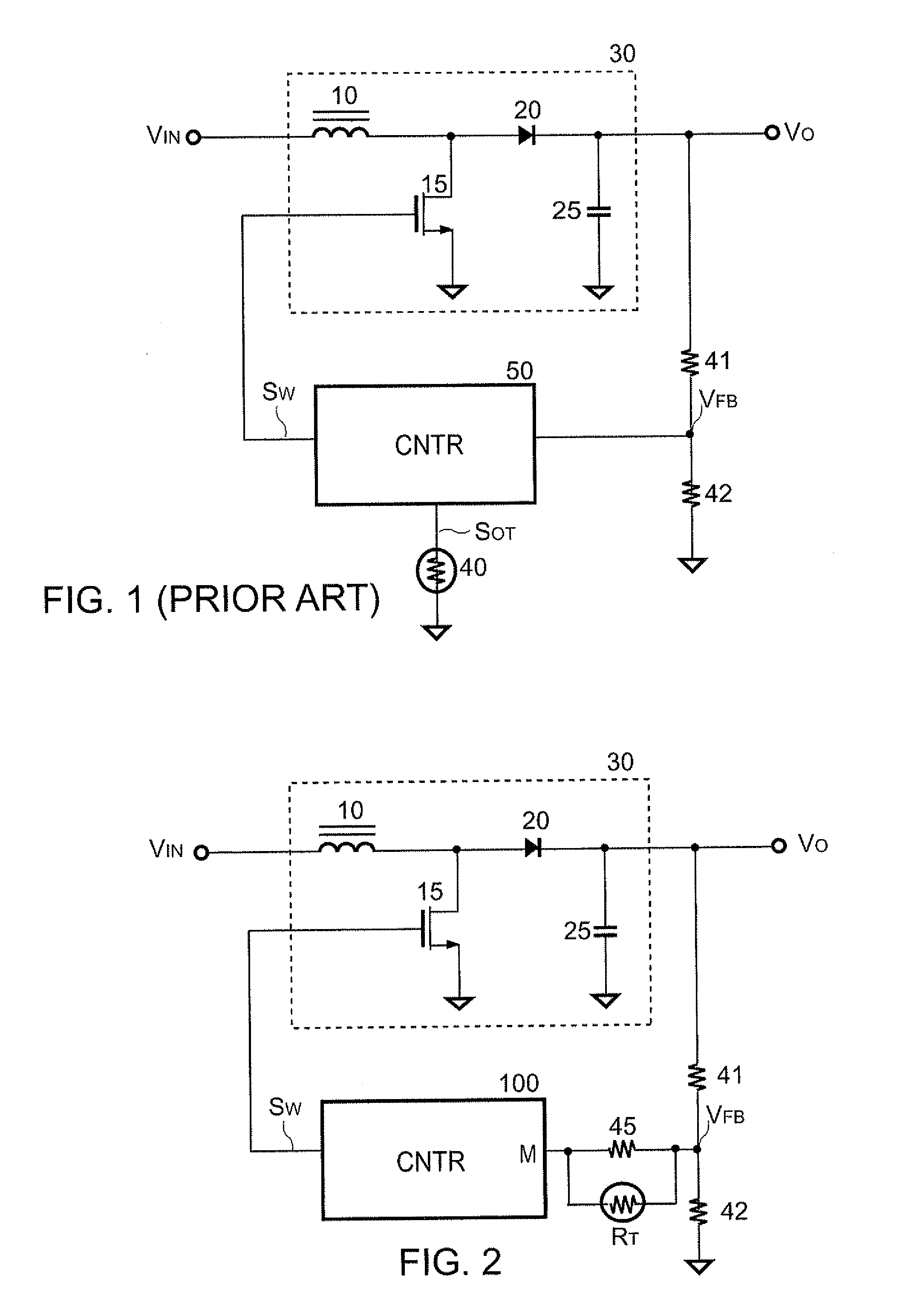
1. Field of Invention The present invention relates to a power converter, and more particularly, the present invention relates to a control circuit having a multi-function terminal of power converter. 2. Description of Related Art The controller 50 generates the switching signal SWto switch the transistor 15 for producing the output voltage VOof the power converter. A feedback signal VFBis generated at a joint of the resistors 41 and 42 of the voltage divider in response to the output voltage VO. The feedback signal VFBis applied to a feedback terminal FB (not shown) of the controller 50 for generating the switching signal SWand regulating the output voltage VO. An over-temperature signal SOTis generated from the thermal device 40 coupled to the controller 50 for over-temperature protection. That is to say, the controller 50 performs over-temperature protection in accordance with the over-temperature signal SOTgenerated by the thermal device 40. An object of the present invention is to provide a multi-function terminal for a switching power supply controller. This terminal is utilized to receive a feedback signal and connect to a thermal device for over-temperature protection. To achieve the aforementioned object, the present invention provides a control circuit having the multi-function terminal, comprising: a switching circuit, the switching circuit generating a switching signal in response to a feedback signal; a sample-and-hold circuit, the sample-and-hold circuit coupled to the multi-function terminal for generating a sample voltage by sampling the feedback signal during a first period; a detection circuit, the detection circuit coupled to the multi-function terminal during a second period for generating a detection voltage; and a comparator, the comparator comparing the detection voltage and the sample voltage for generating an over-temperature signal, wherein the over-temperature is couple to disable the switching signal. The aforementioned first period is disabled when the second period is enabled. To achieve the aforementioned object, the present invention further provides a control circuit having a multi-function terminal, comprising: a switching circuit, generating a switching signal; a plurality of function circuits, coupled to the multi-function terminal and generating a plurality of function signals based on a signal on the multi-function terminal; and a comparator, comparing the function signals for generating an output signal to disable the switching circuit generating the switching signal. The rest of the aforementioned function circuits are disabled when one of the aforementioned function circuits is enabled. The switching circuit is formed by an error amplifier 110, a capacitor 115, an oscillation circuit (OSC) 130, a comparator 120, an inverter 140, a flip-flop 145 and an AND gate 150. The oscillation circuit 130 generates a pulse signal PLS, a ramp signal RMP, the first timing signal S1, a second timing signal S2and a third timing signal S3. The sample voltage VSPgenerated across the capacitor 103 is coupled to a negative input of the error amplifier 110 when the switch 102 controlled by the first timing-signal S1is turned on. A positive input of the error amplifier 110 has a reference signal VRfor the output regulation. An output of the error amplifier 110 is coupled to one terminal of the capacitor 115 for the frequency compensation. The Other terminal of the capacitor 115 is coupled to the ground. The output of the error amplifier 110 is further coupled to a positive input of the comparator 120. The ramp signal RMP is supplied to a negative input of the comparator 120. Comparing the ramp signal RMP with a signal at the output of the error amplifier 110, a reset signal is generated at an output of the comparator 120 to reset the flip-flop 145. A reset input R of the flip-flop 145 receives the reset signal once the ramp signal RMP is larger than the signal at the output of the error amplifier 110. An input of the inverter 140 receives the pulse signal PLS. An output of the inverter 140 is coupled to a clock input CK of the flip-flop 145. That is to say, the oscillation circuit 130 generates the pulse signal PLS to turn on the flip-flop 145 via the inverter 140. The output of the inverter 140 and an output of the flip-flop 145 are connected to the AND gate 150 respectively for generating a switching signal SWwith a switching cycle. The pulse signal PLS provides a limitation to a maximum on-time period of the switching signal SW. The detection circuit is developed by a switch 105 and a current source 106. One terminal of the switch 105 is coupled to the multi-function terminal M. The other terminal of the switch 105 is coupled to one terminal of the current source 106. The other terminal of the current source 106 is coupled to the ground. In other words, the current source 106 is coupled to the multi-function terminal M via the switch 105. A detection voltage (second function signal) VMwill be generated at the multi-function terminal M when the switch 105 controlled by the second timing-signal S2is turned on and a current I106determined by the current source 106 is flowed into the multi-function terminal M. That is to say, the current source 106 is associated with the thermal device RTto generate the detection voltage VM. The detection voltage VMis generated during a second period generated by an on-time period of the second timing signal S2. The one terminal of the capacitor 103 is further coupled to a positive input of the comparator 160. The sample voltage VSPgenerated across the capacitor 103 is applied to the positive input of the comparator 160 during the first period generated by an on-time period of the first timing signal S1. A negative input of the comparator 160 is coupled to the multi-function terminal M through an over-temperature threshold 165. An over-temperature signal SOTgenerated at an output of the comparator 160. The over-temperature signal SOTwill be latched into the flip-flop 145. The comparator 160 compares the detection voltage VM. with the sample voltage VSPfor generating the over-temperature signal SOT. The over-temperature signal SOTis used to disable the switching signal SW. In addition, the control circuit 100 further comprises the over-temperature threshold 165 for generating the over-temperature signal SOT. The oscillation circuit 130 generates the timing signals S1, S2and S3once the switching signal SWis disabled. When the first timing signal S1is enabled and the second timing signal S2is disabled, the feedback signal Valis sampled into the capacitor 103. In the meantime, the switch 102 is turned on and the switch 105 is turned off. The sample-and-hold circuit developed by the switch 102 and the capacitor 103 generates the sample voltage VSPby sampling the feedback signal VFBduring the first period. When the second timing signal S2is enabled, the first timing-signal S1is disabled, the current I106determined by the current source 106 is flowed into the multi-function terminal M. The detection voltage VMwill be applied to the negative input of the comparator 160 via the over-temperature threshold 165. In the meantime, the switch 102 is turned off and the switch 105 is turned on. Therefore, the comparator 160 is utilized to generate the over-temperature signal SOTby comparing the detection voltage VMwith the sample voltage VSP. The over-temperature signal SOTis enabled once the value of the sample voltage VSPis lower than the value of the detection voltage VM. The feedback signal VFBis divided by the output voltage VOthrough the voltage divider. The feedback signal VFBcan be written by the following, The equivalent resistance RDis determined by the resistors 41 and 42. The equivalent resistance RPTis determined by the resistor 45 and the thermal device RT. The equivalent resistance REQis generated by the equivalent resistance RDplus the equivalent resistance RPTas below, The equivalent voltage VDPis generated by the current I106and the equivalent resistance REQas below, The detection voltage VMis generated by the feedback signal VFBminus the equivalent voltage VDPas below, The detection voltage VMwill be generated at the multi-function terminal when the current I106is flowed into the multi-function terminal M. The control circuit 100 further comprises a flip-flop 170. An input D of the flip-flop 170 is coupled to the output of the comparator 160 for receiving the over-temperature signal SOT. A clock input CK of the flip-flop 170 receives the third timing signal S3to trigger the flip-flop 170. A reset input R of the flip-flop 170 is rested by a signal RST. An output Q of the flip-flop 170 is connected to an input D of the flip-flop 145 for controlling the switching signal SWin accordance with the over-temperature signal SOT When the temperature on the power converter is at a low level, the resistance of the thermal device RTis increased because the thermal device RThas a negative temperature coefficient as mentioned previously. The equivalent resistances RPTand REQare increased accordingly. The equivalent voltage VDPis thus increased and the detection voltage VMwill be decreased. Since the equivalent voltage VDPis higher than the over-temperature threshold 165, the over-temperature signal SOTgenerated by the output of the comparator 160 will be logic-high level. The signal STis a logic-high level once the over-temperature signal SOTis a logic-high level and the third timing signal S3is enabled. The flip-flop 145 is thus enabled for generating the switching signal SW. On the other hand, the resistance of the thermal device RTis decreased when the temperature on the power converter is at a high level. The equivalent resistances RPTand REQare decreased accordingly. The equivalent voltage VDPis thus decreased and the detection voltage VMwill be increased. Since the equivalent voltage VDPis lower than the over-temperature threshold 165, the over-temperature signal SOTgenerated by the output of the comparator 160 will be a logic-low level. The signal STis a logic-low level once the over-temperature signal SOTis a logic-low level and the flip-flop 170 is disabled. The flip-flop 145 and the switching signal SWare thus disabled for over-temperature protection. Based on the present invention, an additional terminal is not required to be added the control circuit 100. Therefore, the terminals of the control circuit 100 can be reduced and cost for production will also be reduced. The present invention provides a control circuit having a multi-function terminal. The control circuit comprises a switching circuit, a sample-and-hold circuit, a detection circuit, and a comparator. The sample-and-hold circuit is coupled to the multi-function terminal for generating a sample voltage by sampling the feedback signal during a first period. The detection circuit is coupled to the multi-function terminal during a second period for generating a detection voltage. The comparator compares the detection voltage and the sample voltage for generating an over-temperature signal, wherein the over-temperature signal is couple to disable the switching signal. 1. A control circuit having a multi-function terminal, comprising:
a switching circuit the switching circuit generating a switching signal in response to a feedback signal; a sample-and-hold circuit, the sample-and-hold circuit coupled to the multi-function terminal for generating a sample voltage by sampling the feedback signal during a first period; a detection circuit, the detection circuit coupled to the multi-function terminal during a second period for generating a detection voltage; and a comparator, the comparator comparing the detection voltage and the sample voltage for generating an over-temperature signal, wherein the over-temperature is couple to disable the switching signal. 2. The control circuit as claimed in 3. The control circuit as claimed in 4. The control circuit as claimed in 5. The control circuit as claimed in 6. The control circuit as claimed in 7. The control circuit as claimed in 8. The control circuit as claimed in 9. The control circuit as claimed in 10. The control circuit as claimed in 11. The control circuit as claimed in 12. A control circuit having a multi-function terminal, comprising:
a switching circuit, generating a switching signal; a plurality of function circuits, coupled to the multi-function terminal and generating a plurality of function signals based on a signal on the multi-function terminal; and a comparator, comparing the function signals for generating an output signal to disable the switching circuit generating the switching signal. 13. The control circuit as claimed in 14. The control circuit as claimed in 15. The control circuit as claimed in 16. The control circuit as claimed in 17. The control circuit as claimed in BACKGROUND OF THE INVENTION
SUMMARY OF THE INVENTION
BRIEF DESCRIPTION OF THE DRAWINGS
DESCRIPTION OF THE PREFERRED EMBODIMENTS