THREE-PHASE AC TO DC CONVERTER AND AIR CONDITIONING APPARATUS USING THREE-PHASE AC TO DC CONVERTER
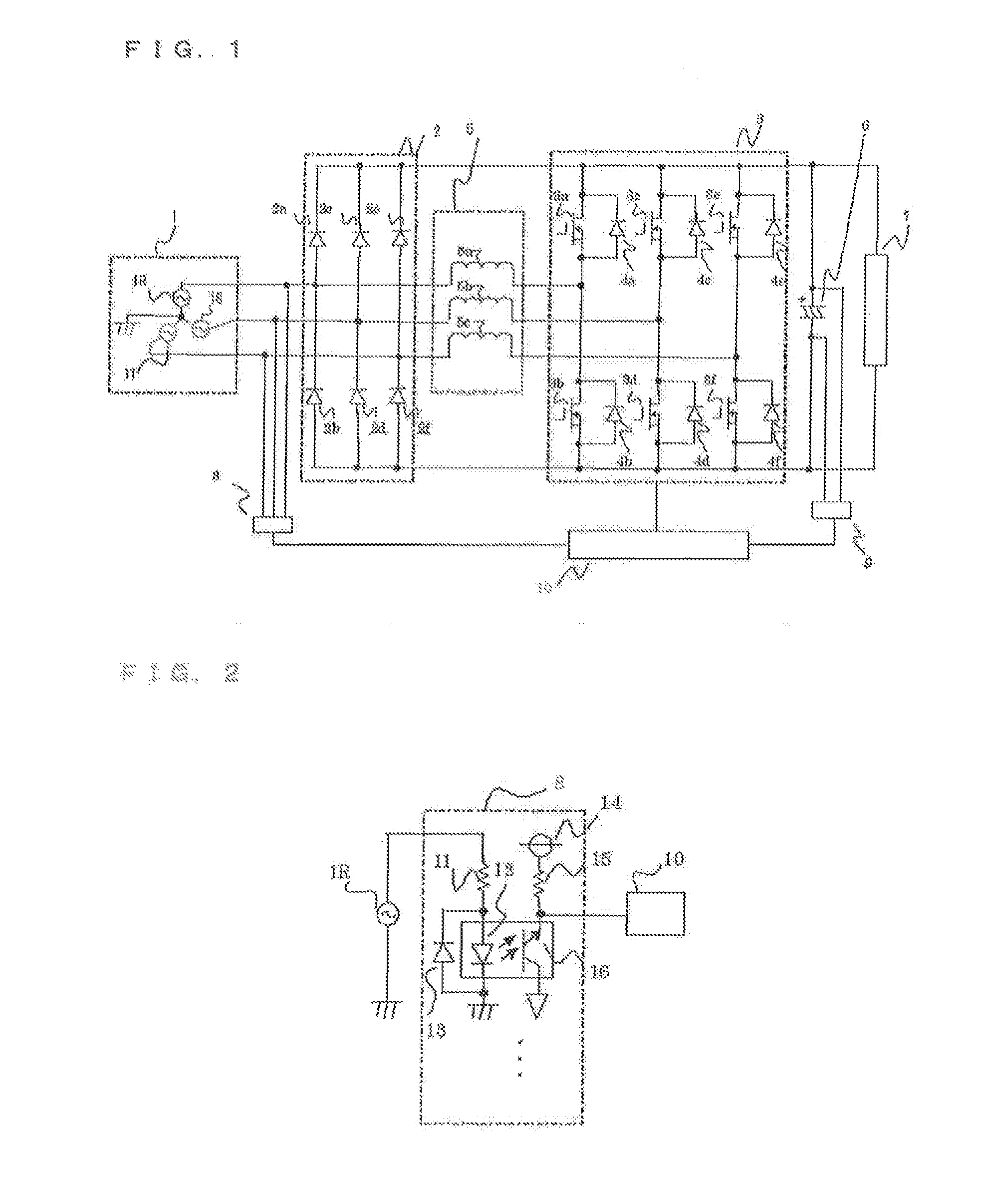
The present invention relates to a three-phase alternating current (AC) to direct current (DC) converter that converts three-phase AC power to DC power, and an air-conditioning apparatus using the three-phase AC to DC converter. In general, industrial air-conditioning apparatuses larger than domestic air-conditioning apparatuses use three-phase AC power. In such an industrial air-conditioning apparatus, an inverter is usually used to drive a load, such as a motor, provided in the air-conditioning apparatus. Since the input to the inverter needs to be DC voltage, it is necessary to convert three-phase AC power to DC power. There have been proposed various apparatuses that convert three-phase AC power to DC power. For example, Patent Literature 1 discloses a boost three-phase full-wave rectifier that includes a circuit breaker capable of disconnecting three-phase AC power, a current detector configured to detect phase currents flowing through respective phase lines, boost inductors provided for the respective phase lines, a three-phase full-wave rectifying circuit including switching semiconductor devices connected in a three-phase bridge configuration, a smoothing capacitor, and a control circuit configured to perform high-frequency switching of the switching semiconductor devices according to a predetermined sequence. In this boost three-phase full-wave rectifier, diodes are connected so as to form a three-phase bridge circuit in which the phase lines between the circuit breaker and the respective boost inductors serve as inputs thereof, and positive and negative common lines of the three-phase full-wave rectifying circuit serve as outputs thereof. However, such a three-phase AC to DC converter in related art determines whether to turn on or turn off the switching devices on the basis of the current values of the respective phases detected by a current sensor. Therefore, the three-phase AC to DC converter in related art has low followability with respect to voltage changes, and is susceptible to the sensor characteristics such as frequency response and temperature drift. This results in harmonic leakage current and generation of noise. Furthermore, the current sensor is often a through-type current sensor. In this case, the current path to be measured needs to be inserted through the current sensor, resulting in an increase in the mounting cost and the cost of the sensor itself. These problems become more pronounced particularly in the case where the three-phase AC to DC converter is applied to apparatuses having an inverter load, such as air-conditioning apparatuses. The invention has been made to overcome the above problems, and aims to provide a three-phase AC to DC converter capable of reducing harmonic leakage current and the noise level, and an air-conditioning apparatus using the three-phase AC to DC converter. A three-phase AC to DC converter according to the invention includes a three-phase AC power supply, a three-phase rectifier bridge circuit that is connected to the three-phase AC power supply and that includes rectifying devices which are connected in a bridge configuration between two DC buses, a three-phase full-bridge circuit that includes two serially-connected switching devices for each of three phases, the two serially-connected switching devices being connected between the DC buses at an output side of the three-phase rectifier bridge circuit, and that includes reverse blocking diodes which are connected in parallel to the respective switching devices, a reactor that connects a connection point between the two serially-connected switching devices of each phase to a corresponding phase of the three-phase AC power supply, a smoothing capacitor connected between the DC buses at an output side of the three-phase full-bridge circuit. DC voltage detection means that detects an output voltage between the DC buses, power supply phase detection means that detects a power supply phase of the three-phase AC power supply, and pulse width modulation means that outputs PWM signals which control the switching devices, wherein the pulse width modulation means outputs the PWM signals on the basis of the power supply phase and the output voltage. According to the invention, it is possible to provide a three-phase AC to DC converter capable of reducing harmonic leakage current and the noise level, and an air-conditioning apparatus using the three-phase AC to DC converter. 1 three-phase AC power supply, 2 three-phase rectifier bridge circuit, 2 Referring to A three-phase rectifier bridge circuit 2 includes six diodes 2 Further, an anode side of the diode 2 A three-phase full-bridge circuit 3 includes six FETs 3 Further, the source side of the FET 3 An output side of the three-phase full-bridge circuit 3 is connected to a smoothing capacitor 6, and an output side of the smoothing capacitor 6 is connected to a load 7. Although not illustrated in detail, the load 7 is typically an AC load connected through an inverter. For example, in an air-conditioning apparatus, the load 7 may be a motor that drives a compressor, a fan, and the like. Power supply phase detection means 8 is connected to output sides of the AC power supplies 1R, 1S, and 1T so as to detect respective phases of the R-phase voltage, S-phase voltage, and T-phase voltage. DC voltage detection means 9 is connected to both ends of the smoothing capacitor 6 so as to detect a voltage applied to the smoothing capacitor 6. The pulse width modulation means 10 transmits control signals to the FETs 3 Referring to A constant-voltage power supply 14 is connected to an emitter side of a phototransistor 16 through an output side resistor 15. Further, the phototransistor 16 is connected at a collector side thereof to ground, and is arranged such that the light from the light-emitting diode 12 is made incident on a base thereof. The emitter potential of the phototransistor 16 is output to the pulse width modulation means 10. That is, when the light from the light-emitting diode 12 is made incident on the phototransistor 16, the phototransistor 16 becomes conductive so as to output 0 V to the pulse width modulation means 10. On the other hand, when the light from the light-emitting diode 12 is not made incident on the phototransistor 16, the phototransistor 16 outputs the voltage of the constant-voltage power supply 14 to the pulse width modulation means 10. It is to be noted that, although the circuit configuration for R-phase is illustrated in Since the phases of the three-phase AC power supply are shifted by 120 degrees from each other, the pulse width modulation means 10 may perform an operation of calculating, on the basis of an output for one phase, phases of the other phases. Alternatively, a dedicated device to perform this operation may be separately provided. Further alternatively, phase information of the respective phases may be multiplexed in the power supply phase detection means 8 using known means, such as a microcomputer and a digital circuit, so as to be output to the pulse width modulation means 10. Next, a description will be given of operations. (1) Operations of Power Supply Phase Detection Means 8 First, operations of the power supply phase detection means 8 will be described with reference to Referring to When the R-phase voltage 17R is positive, the R-phase emitter potential 18R is in an L state. When the R-phase voltage 17R is negative, the R-phase emitter potential 18R is in an H state. The same applies to the other phases. However, as mentioned above, since the phases of the AC power supplies 1R, 1S, and 1T are shifted by 120 degrees from each other (more specifically, the S-phase voltage is delayed by 120 degrees from the R-phase voltage, and the T-phase voltage is delayed by 120 degrees from the S-phase voltage), the emitter potentials are also shifted by 120 degrees from each other. The pulse width modulation means 10 can determine in which sections of 60 degrees the phase of the three-phase AC power supply 1 is, on the basis of the state change of the emitter potentials of the respective phases. For example, when the R-phase emitter potential is changed from the H state to the L state (i.e., falls), the phase becomes 0 degree. Thus, the phase is determined to be brought into the section of 0 through 60 degrees. Further, when the R-phase emitter potential is changed from the L state to the H state (i.e., rises), the phase becomes 60 degree. Thus, the phase is determined to be brought into the section of 60 through 120 degrees. Determination of other sections can be made in the same manner. This is summarized in a table as shown in Table 1. The above determination may be made on the basis of the state itself in place of the state change of the emitter potential. For example, when only the S-phase emitter potential is in the H state, the phase is determined to be in Section 1 of 0 through 60 degrees. Further, when only the R-phase emitter potential is in L state, the phase is determined to be in Section 2 of 60 through 120 degrees. Determination of other sections can be made in the same manner. This is summarized in a table as shown in Table 2. (2) Operations of Entire Three-Phase AC to DC Converter Circuit In the following, operations of the entire three-phase AC to DC converter circuit will be described. In Section 1, since only the S-phase voltage is negative and the R-phase voltage and the T-phase voltage are positive, currents flow from R-phase to S-phase, and from T-phase to S-phase, respectively. In this case, the current flows through the following route in accordance with ON and OFF of the FET 3 (When FET 3 AC power supply 1R→reactor 5 (When FET 3 AC power supply 1R→reactor 5 That is, when the FET 3 Further, as describe below, the flow of the current between the T-phase and S-phase is similar to the above, and the smoothing capacitor 6 is charged through accumulation and release of electromagnetic energy in the reactor 5 (When FET 3 AC power supply 1T→reactor 5 (When FET 3 AC power supply 1T→reactor 5 Further, during Section 1, since the diode 2 Then, in Section 2, since only the R-phase voltage is positive and the S-phase voltage and the T-phase voltage are negative, currents flow from R-phase to S-phase, and from R-phase to T-phase, respectively. In this case, in the same manner as described above, current flows through the following route in accordance with ON and OFF of the FET 3 (When FET 3 AC power supply 1R→diode 2 (When FET 3 AC power supply 1R→diode 2 (When FET 3 AC power supply 1R→diode 2 (When FET 3 AC power supply 1R→diode 2 Further, during Section 2, since the diode 2 Similar operations are performed in Section 3 and the subsequent sections. According to Embodiment 1, if the voltage of one of the three phases is negative, the lower arm FETs of the other two phases are PWM-controlled. Also, if the voltage of one of the three phases is positive, the upper arm FETs of the other two phases are PWM-controlled. Thus, an increased DC bus voltage is generated. As described above. FETs to be controlled by the pulse width modulation means 10 are changed from section to section. However, since the FETs are controlled in accordance with the output of the power supply phase detection means 8 which has high followability with respect to changes in the power supply voltage, the harmonic leakage current and the noise level are reduced. (3) Method of Generating Reference Signal of PWM Signal Further, the phase voltages of R-phase, S-phase, and T-phase are displaced from each other by 120 degrees (2π/3[rad]), and therefore are expressed by [Math. 2], where VR, VS, and VT represent the phase voltages of R-phase, S-phase, and T-phase, respectively, and V is the amplitude of the respective phase voltages. Generally, the relationship between the voltage v applied to the inductance L and the current i is expressed by [Math. 3]. The voltage v applied to the inductance L is a phase-to-phase voltage. The variation of the phase-to-phase voltage over time differs in accordance with phase lead or lag between phases. For instance, in the case of controlling the current of R-phase, in Section 1 and Section 4, the phase-to-phase voltage applied to the inductance 5 Further, in the case of controlling the current of R-phase, in Section 3 and Section 6, the phase-to-phase voltage applied to the inductance 5 Accordingly, when PWM control is performed using, as a reference signal, a coefficient α that satisfies [Math. 6] in Sections 1 and 4 and [Math. 7] in Sections 3 and 6, the current of R-phase can be controlled to have a sine wave shape. The reference signal α is calculated by substituting [Math. 1], [Math. 4], and [Math. 5] into each of [Math. 6] and [Math. 7] and using approximation that vRS and vRT are constant in micro time Δt, so that [Math. 8] and [Math. 9] are obtained. Accordingly, in Sections 1 and 4 where the phase-to-phase voltage between the phase to be controlled and the phase delayed by 120 degrees with respect thereto is applied to the reactor of the phase to be controlled, a reference signal proportional to sin ωt/sin(ωt+π/6) is used. On the other hand, in Sections 3 and 6 where the phase-to-phase voltage between the phase to be controlled and the phase advanced by 120 degrees with respect thereto is applied to the reactor of the phase to be controlled, a reference signal proportional to sin ωt/sin(ωt−π/6) is used. Thus, the current of R-phase can be controlled to have a substantially sine wave shape. It is to be noted that the amplitude of the reference signal may be determined using a known control method such that the DC voltage detected by the DC voltage detection means 9 and the target value of the DC voltage is reduced. It is to be noted that, the variation range of the power supply phase θ (i.e., ωt) in [Math. 8] and [Math. 9] is one period of 0 through 2π (0 through 360 degrees). However, as shown below, if the variation range of the power supply phase θ is set to the above-described sections of 60 degrees each, the reference signal can be more easily generated. More specifically, no change is made to [Math. 8] with regard to Section 1. However, with regard to Section 3, which starts from 120 degrees (2π/3) in the entire period, ωt is replaced with ωt+2π/3 in [Math. 9], so that [Math. 10] is obtained. Further, in [Math. 8] and [Math. 9], sin α=−sin(α+π) holds, and a sin function appears in both the numerator and denominator. This indicates that [Math. 8] and [Math. 9] are functions each having a period of π. Accordingly, [Math. 8] is applicable to Section 1 and Section 4 which is phase-shifted therefrom by 180 degrees, and [Math. 10] is applicable to Section 3 and Section 6 which is phase-shifted by 180 degrees. As can be seen from the above, in the case where the variation range of the power supply phase θ is divided into the above-described sections of 60 degrees each, if a reference signal proportional to sin ωt/sin(ωt+π/6) is used in Sections 1 and 4 where the phase-to-phase voltage between the phase to be controlled and the phase delayed 120 degrees with respect thereto is applied to the reactor of the phase to be controlled, and if a reference signal proportional to sin(ωt+2π/3)/sin(ωt+π/2) is used in Sections 3 and 6 where the phase-to-phase voltage between the phase to be controlled and the phase advanced by 120 degrees with respect thereto is applied to the reactor to be controlled, the current of R-phase can be controlled to have a substantially sine wave shape. It is to be noted that the amplitude of the reference signal may be using a known controlled such that the DC voltage detected by the DC voltage may be selected using a known control method such that the difference between the DC voltage detected by the DC voltage detection means 9 and the target value of the DC voltage is reduced. According to Embodiment 1, since the followability with respect to voltage changes is improved by performing the PWM control on the basis of the phase detected by the phase detection means, it is possible to obtain a three-phase AC to DC converter capable of reducing harmonic leakage current and the noise level. Also, since the phase detection means is formed of diodes and a photo coupler, it is possible to detect the power supply phase by using a simple and inexpensive circuit. Also, since the transistor of the photo coupler is not used for analog operations in the unsaturated region, but is user for switching operations in the saturated region, it is possible to reduce adverse effects on the transfer characteristics due to the variations in the device characteristics and the changes over time. Further, the switching control is performed with a simple configuration based only on the input power supply phase and the DC bus voltage value, and therefore can be realized with a small number of sensors and an inexpensive microcomputer. In particular, since the reference signal used for PWM control for making the input current have a substantially sine wave shape is expressed by a simple expression in which the phase is the only variable, the associated circuits such as a sensor as well as software installed in the microcomputer are simplified, so that an inexpensive configuration can be realized. Further, since the phase is the only variable, the reference signal is a stable and repetitive output. Therefore, although precise accuracy with respect to power-supply variations, load variations, or the like might not be obtained, there is no need to perform additional protection control against overcurrent in a transient response upon feedback of current or the like. Therefore, this system is simple and inexpensive in this regard as well. Further, since the phase detection means has high followability, the switching operation of the FETs can be performed at a higher speed. Since the switching operation of the FETs can be performed at a higher speed, the controllable range of the target voltage value can be increased. Furthermore, since the switching operation of the FETs can be performed at a higher speed, the inductance value of the reactor can be reduced, which makes it possible to reduce the size of the reactor. However, in the circuit configuration according to Embodiment 1, if switching devices are operated at a high speed, there arises a new problem of increased heat generation by the switching devices. The circuit configuration in related art does not have this problem because, in the first place, it is not possible to operate switching devices at a high speed with the circuit configuration in related art. In this case, a wide bandgap semiconductor such as SiC (silicon carbide) may be used as a switching device. A wide bandgap semiconductor is a semiconductor that uses a device having a greater bandgap than a Si device. Examples of wide bandgap semiconductors include SiC, GaN (gallium nitride), and a diamond device. The wide bandgap semiconductor can operate at a high speed, and has a higher heat-resistant temperature than Si devices. Accordingly, if wide bandgap semiconductors are used as the switching devices in the circuit configuration of Embodiment 1, it becomes possible to operate switching devices at a high speed. Further, since the wide bandgap semiconductor has a higher heat-resistant temperature than a Si device, it becomes possible to reduce the size of a radiator fin or to realize a configuration without a radiator fin. In the case where a wide bandgap semiconductor such as SiC is used, from the viewpoint of emission regulations on EMC such as noise terminal voltage (e.g., EN61000-6-3: 2007, J55014-1 (H20), and VCCI (2008.4) Class A), the carrier frequency of the triangular wave that generates a PWM signal may be set such that the carrier frequency and a sideband wave thereof do not overlap the frequencies specified in the regulations. For instance, since the lower limit frequency set by the noise terminal voltage regulations is 150 kHz, the carrier frequency of the triangular wave that generates a PWM signal may be set to about 73 kHz, which is less than one-half of 150 kHz, about 49 kHz, which is less than one-third of 150 kHz, or about 36 kHz, which is less than one-fourth of 150 kHz, such that the sideband wave having a frequency equal to an integral multiple of the carrier frequency becomes slightly less than 150 kHz. It is to be noted that, since the three-phase AC to DC converter of Embodiment 1 can reduce harmonic leakage current and the noise level, if this three-phase AC to DC converter is applied to electrical equipment, such as an air-conditioning apparatus, having an inverter load, it is possible to reduce the current flowing to the ground through a stray capacitance Cm, and therefor to reduce leakage current and the noise terminal voltage. The triangular waves used for generation of PWM signals may be triangular waves having phases opposite to each other in two phases where switching operations are performed. Although the current flowing through the rectifying bridge circuit is the sum of the currents flowing in these respective phases, since these phases have phase opposite to each other, current ripples also have phases opposite to each other. Thus, the distorted current can be reduced. Although the PWM control using a simple system is illustrated in the above description, if tracking control based on feedback of the input current is used, unbalance and distortion of the input power supply voltage can be handled, making it possible to perform control with higher accuracy. In this case, the cost and the complexity are increased. Accordingly, the cost effectiveness may be selected in accordance with the load capacity, the regulation value, and the effects on the ambient environment. Further, although the frequency of the triangular wave to be compared with the reference signal upon generation of a PWM control signal may be a fixed frequency, the frequency may be made variable by having frequency jitter, for example. In this case, frequency dispersion is achieved while preventing the radiation noise from the main circuit from concentrating on a certain frequency. Thus, the peak of the radiation noise can be reduced. In More specifically, the FETs 3 Further, the source side of the FET 3 Although the operations are substantially the same as those of Embodiment 1, there is a difference in that, upon generating PWM signals for controlling FETs that are connected in parallel in each phase, PWM signals are generated based on triangular waves having phases opposite to each other. It is to be noted that, although R-phase will be described below, the same applies to the other phases. Among PWM signals generated in the manner described above, the PWM signal 23 is output so as to control the FET 3 It is to be noted that, although a set of two parallelly-connected FETs is used for control a single phase in Embodiment 2, a set of three or more parallelly-connected FETs may be used for controlling a single phase. In this case, a set of parallelly-connected FETs may be divided into two sub-sets such that the FETs in one of the sub-sets are controlled by the PWM signal 23 which is generated using the triangular wave 22 and such that the FETs in the other one of the sub-sets are controlled by the PWM signal 23′ which is generated using the triangular wave 22′ having a phase opposite to that of the triangular wave 22. With this control, currents flowing through the parallelly-connected reactors 5 The invention is widely applicable to apparatuses that convert a three-phase alternating current into a direct current. In particular, the invention is widely applicable to electric apparatuses having an inverter load, such as air-conditioning apparatuses, refrigerators, freezers, and heat pump water heaters. A three-phase AC to DC converter includes a three-phase AC power supply, a three-phase rectifier bridge circuit that is connected to the three-phase AC power supply and includes rectifying devices which are connected in a bridge configuration, a three-phase full-bridge circuit that includes two serially-connected switching devices for each of three phases, the two serially-connected switching devices being connected at an output side of the three-phase rectifier bridge circuit, and includes reverse blocking diodes which are connected in parallel to the respective switching devices, a reactor that connects the three-phase full-bridge circuit to the three-phase AC power supply, a smoothing capacitor connected to an output side of the three-phase full-bridge circuit, DC voltage detection means that detects an output voltage, power supply phase detection means that detects a power supply phase of the three-phase AC power supply, and pulse width modulator that outputs PWM signals which control the switching devices. 1. A three-phase AC to DC converter comprising:
a three-phase AC power supply; a three-phase rectifier bridge circuit that is connected to the three-phase AC power supply, and that includes rectifying devices which are connected in a bridge configuration between two DC buses; a three-phase full-bridge circuit that includes two serially-connected switching devices for each of three phases, the two serially-connected switching devices being connected between the DC buses at an output side of the three-phase rectifier bridge circuit, and that includes reverse blocking diodes which are connected in parallel to the respective switching devices; a reactor that connects a connection point between the two serially-connected switching devices of each phase to a corresponding phase of the three-phase AC power supply; a smoothing capacitor connected between the DC buses at an output side of the three-phase full-bridge circuit; DC voltage detection means that detects an output voltage between the DC buses; power supply phase detection means that detects a power supply phase of the three-phase AC power supply; and pulse width modulation means that outputs PWM signals which control the switching devices wherein the pulse width modulation means outputs the PWM signals on the basis of the power supply phase and the output voltage. 2. The three-phase AC to DC converter of the power supply phase detection means includes: a light-emitting diode connected to the three-phase AC power supply; and a phototransistor that is connected to a constant-voltage power supply through a resistor and that is configured to perform switching operation in response to light emitted from the light-emitting diode. 3. The three-phase AC to DC converter of the pulse width modulation means is configured to output, when only one phase of the three-phase AC power supply has a positive voltage, the PWM signals to switching devices located at an upper arm side among the two serially-connected switching devices that control other two phases, and output, when only one phase of the three-phase AC power supply has a negative voltage, the PWM signals to switching devices located at a lower arm side among the two serially-connected switching devices that control other two phases. 4. The three-phase AC to DC converter of the pulse width modulation means generates a reference signal proportional to an expression in which the power supply phase is an only variable, and outputs a PWM signal on the basis of a comparison between the reference signal and a triangular wave. 5. The three-phase AC to DC converter of in a case where one period of the power supply phase is divided into sections by 60 degrees each and a power supply phase for each section is denoted by θ, when a phase-to-phase voltage between a phase to be controlled and a phase delayed with respect thereto is applied to a reactor of the phase to be controlled, the reference signal is proportional to)sin θ/sin(θ+30°); and when a phase-to-phase voltage between the phase to be controlled and a phase advanced with respect thereto is applied to the reactor of the phase to be controlled, the reference signal is proportional to sin(120°+θ)/sin(90°+θ). 6. The three-phase AC to DC converter of the three-phase full-bridge circuit includes a plurality of sets of the two serially-connected switching devices for each of the phases, the plurality of sets being connected in parallel to each other between the DC buses; and a connection point between the two serially-connected switching devices of each phase is connected to the corresponding phase of the three-phase AC power supply with the reactor. 7. The three-phase AC to DC converter of the pulse width modulation means generates two of the PWM signals using triangular waves which have phases opposite to each other, one of the PWM signals controls half of switching devices included in the plurality of sets of the two serially-connected switching devices of one of the phases, and another one of the PWM signals controls switching devices included in the plurality of sets of the two serially-connected switching devices of the remaining one of the phases. 8. The three-phase AC to DC converter of the switching devices include wide bandgap semiconductors. 9. The three-phase AC to DC converter of 10. An air-conditioning apparatus to which a motor of a compressor is connected as a load of the three-phase AC to DC converter of TECHNICAL FIELD
BACKGROUND ART
CITATION LIST
Patent Literature
DISCLOSURE OF INVENTION
Technical Problem
Solution to Problem
Advantageous Effects of Invention
BRIEF DESCRIPTION OF DRAWINGS
REFERENCE SIGNS LIST
BEST MODE FOR CARRYING OUT THE INVENTION
Embodiment 1
section 1 2 3 4 5 6 phase 0-60 60-120 120-180 180-240 240-300 300-360 conditions R-phase T-phase S-phase R-phase T-phase S-phase fall rise fall rise fall rise section 1 2 3 4 5 6 phase 0-60 60-120 120-180 180-240 240-300 300-360 conditions Only Only Only Only Only Only S-phase R-phase T-phase S-phase R-phase T-phase is is in H is in L is in H is in L is in H in L state state state state state state Embodiment 2
INDUSTRIAL APPLICABILITY