SWITCH CIRCUIT, RADIO-FREQUENCY MODULE, AND COMMUNICATION DEVICE
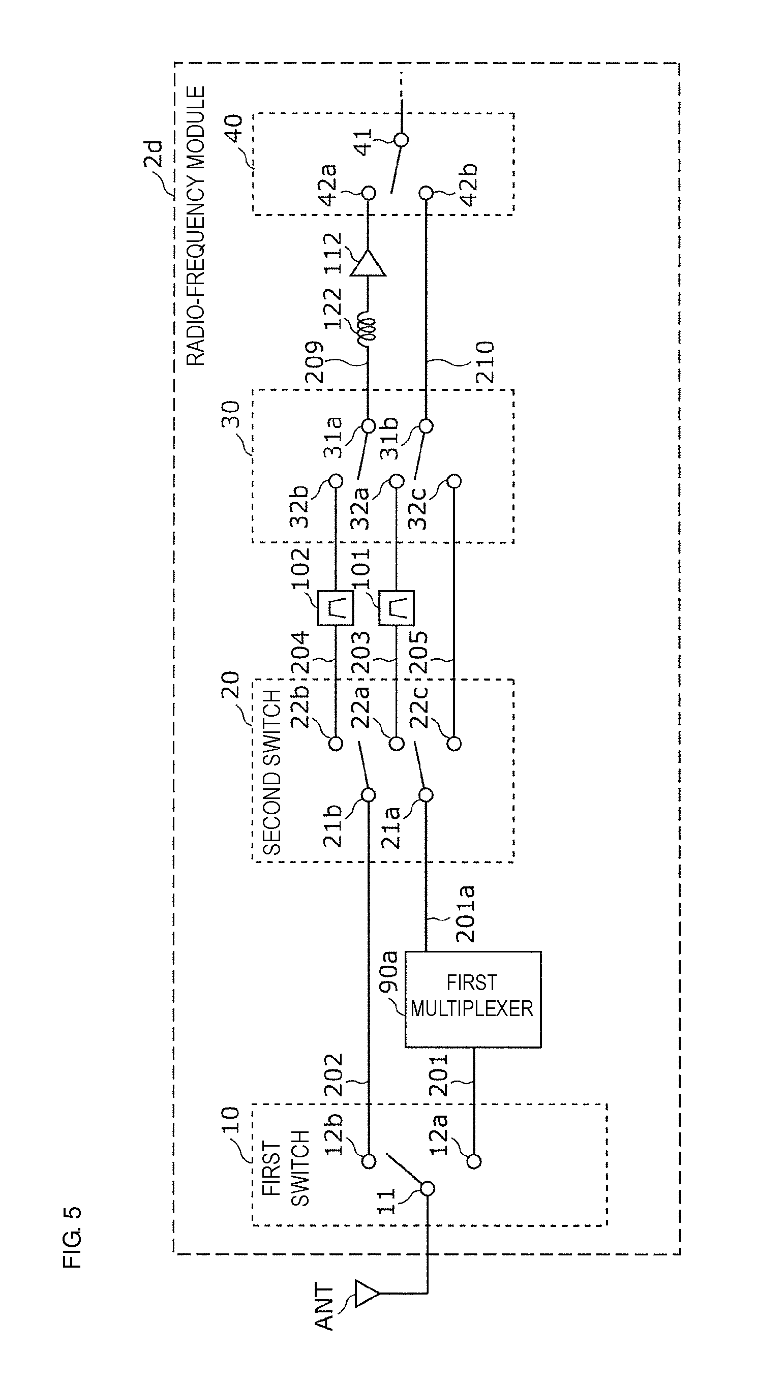
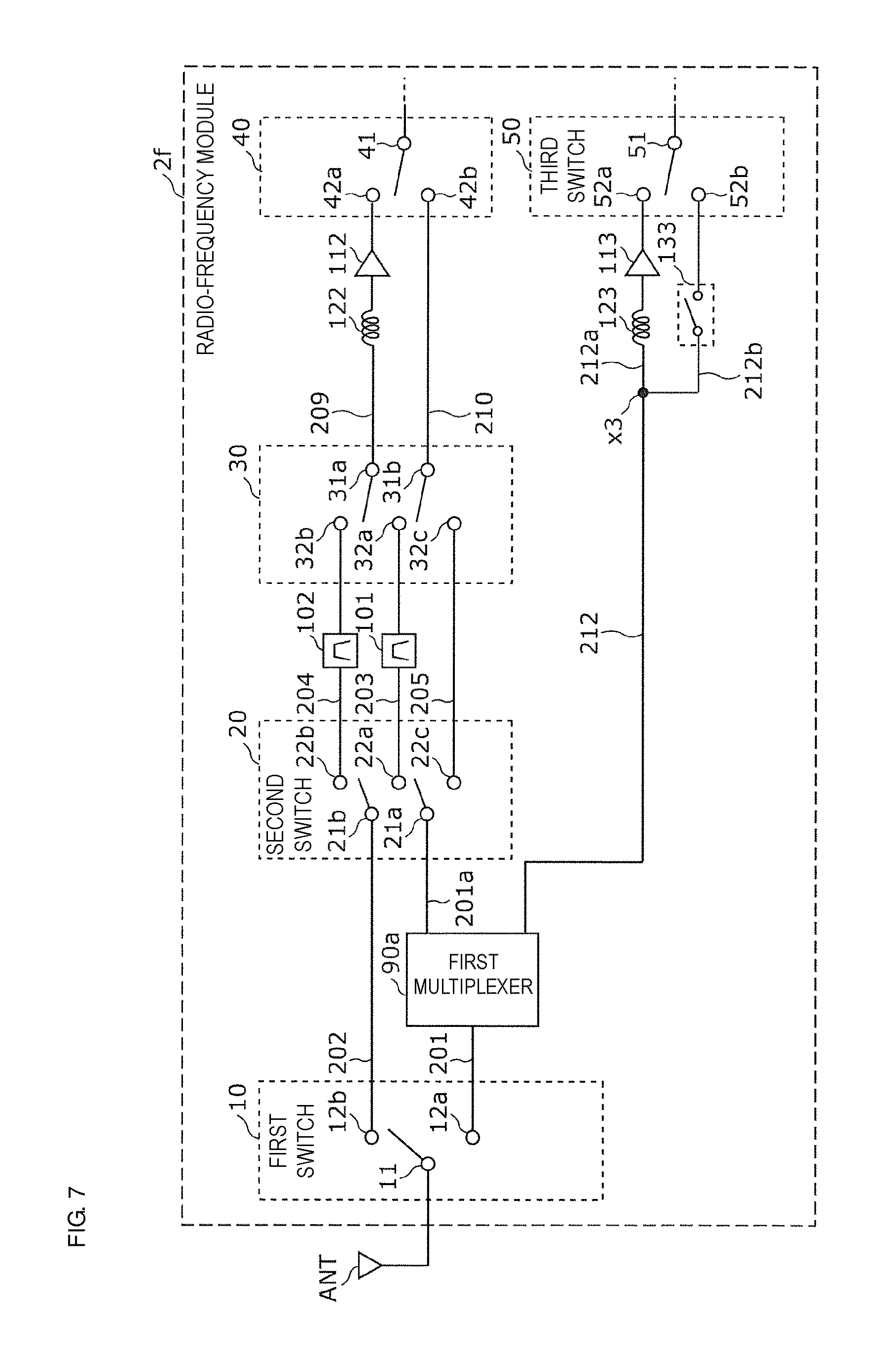
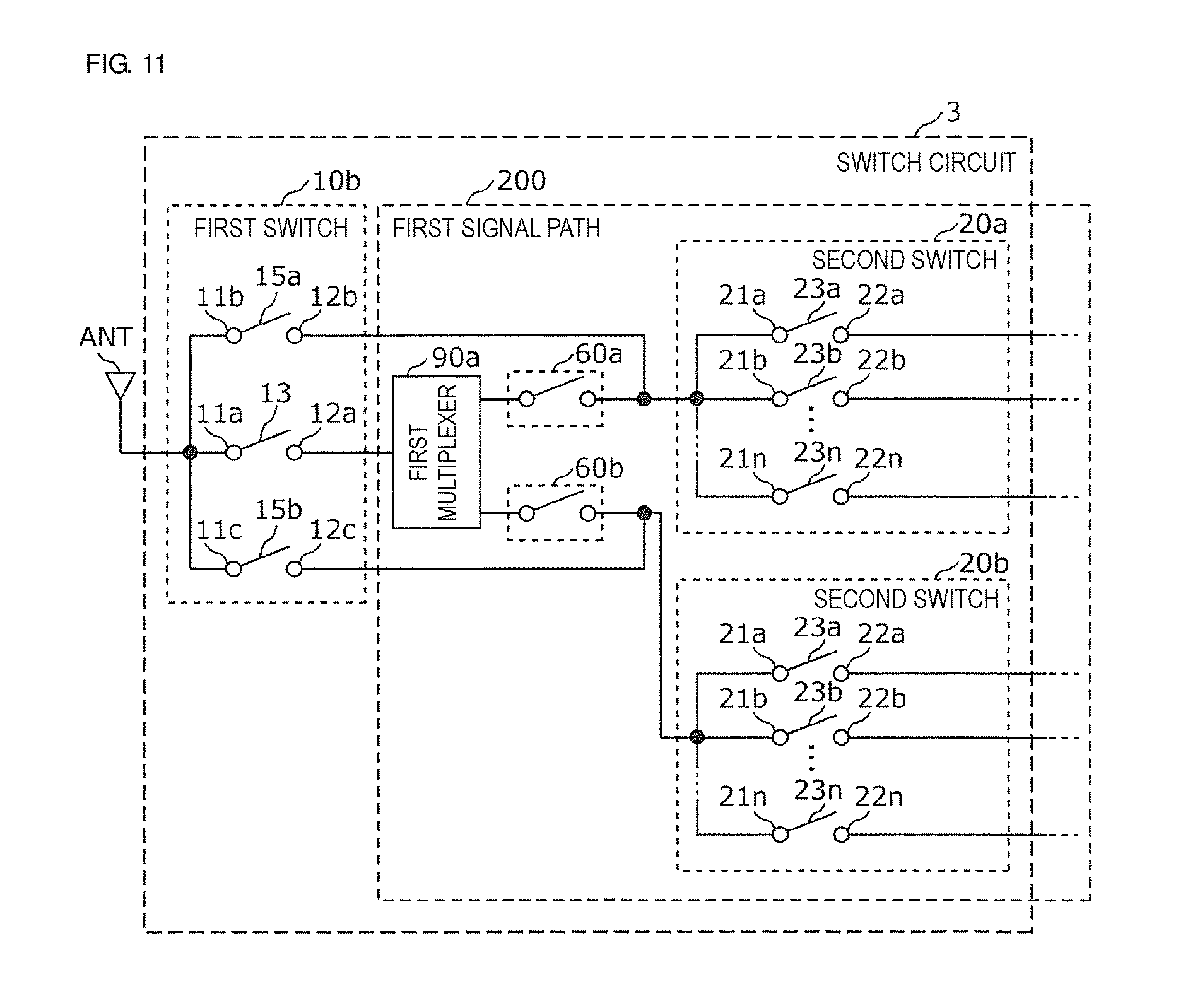
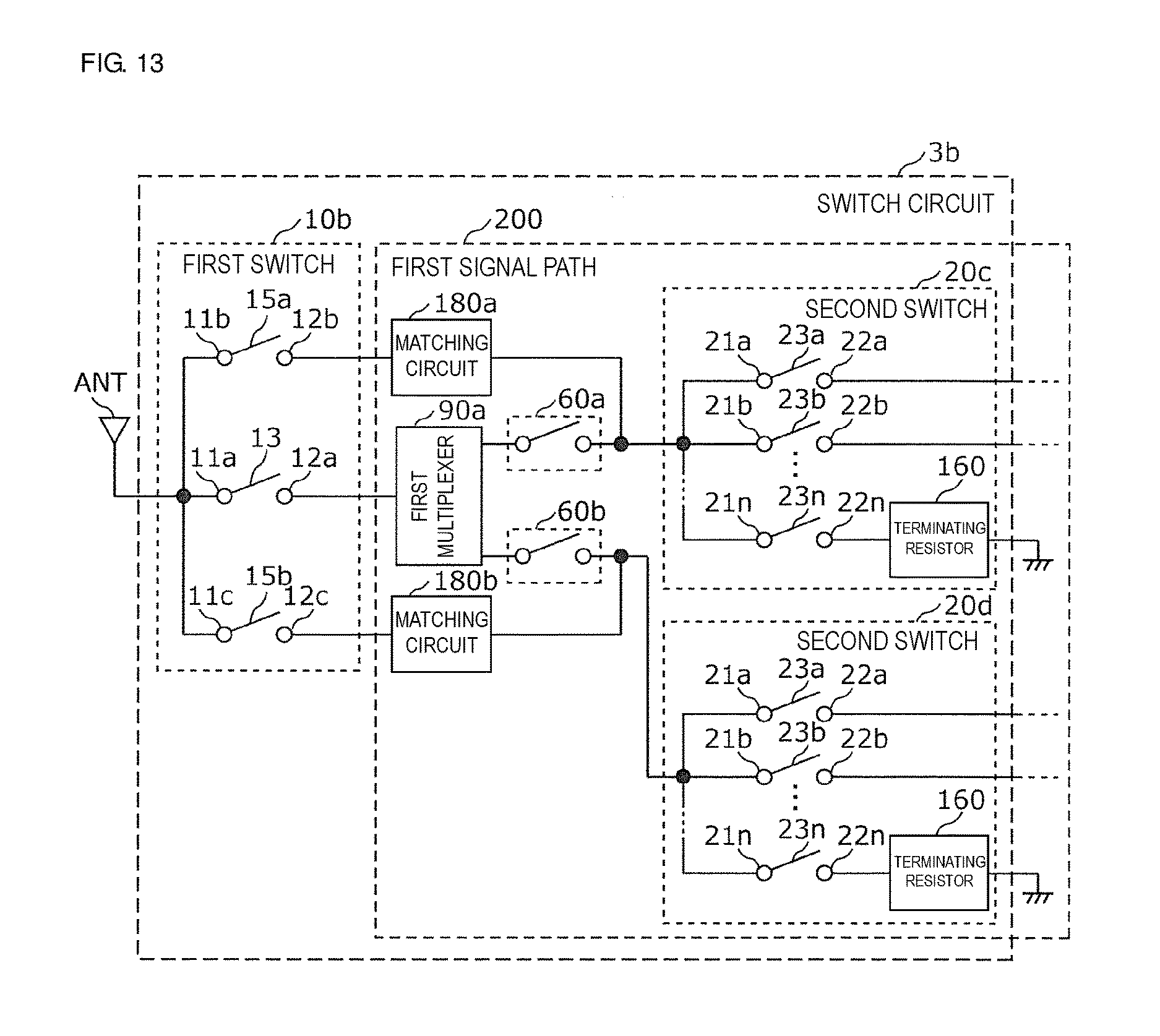
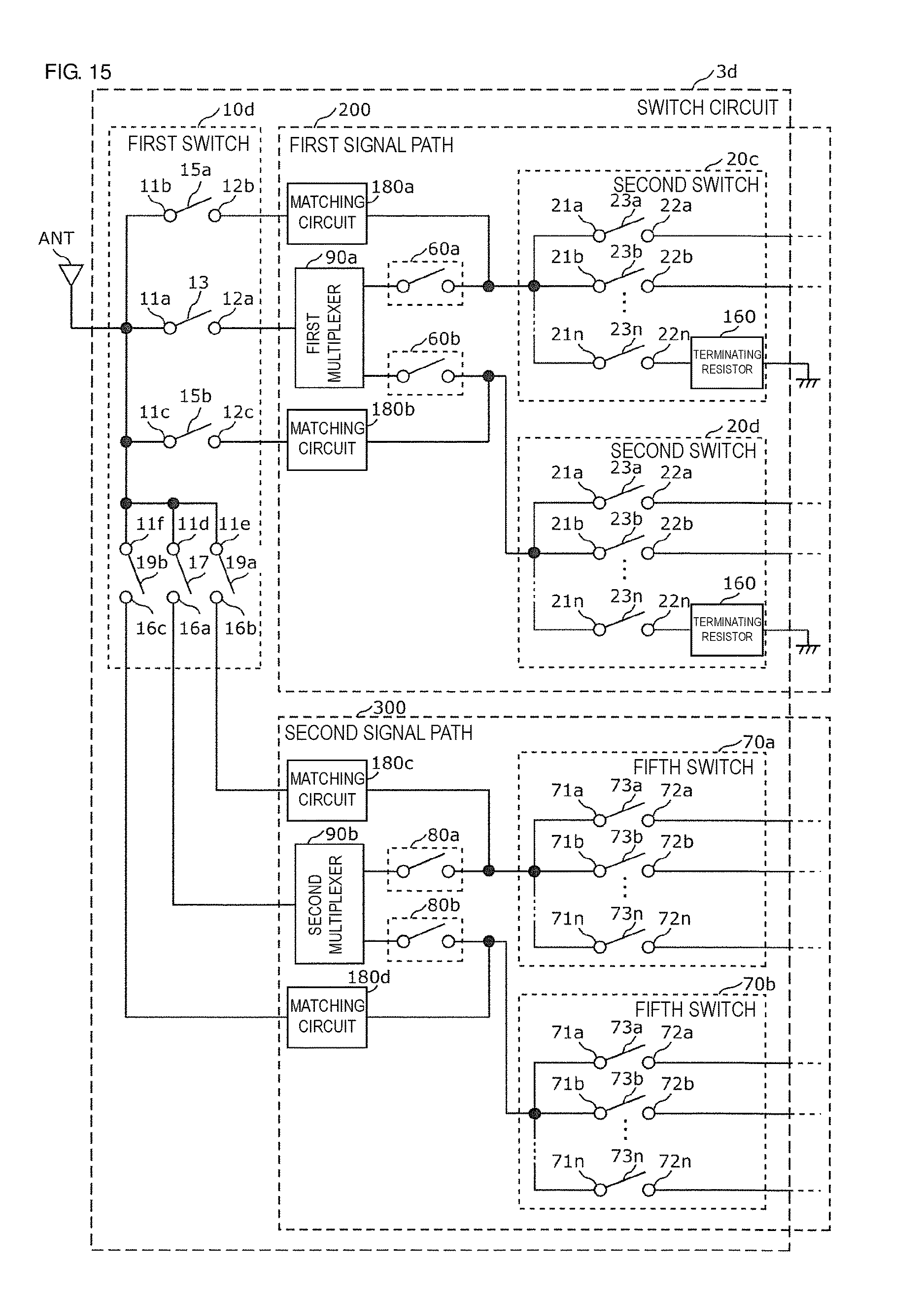
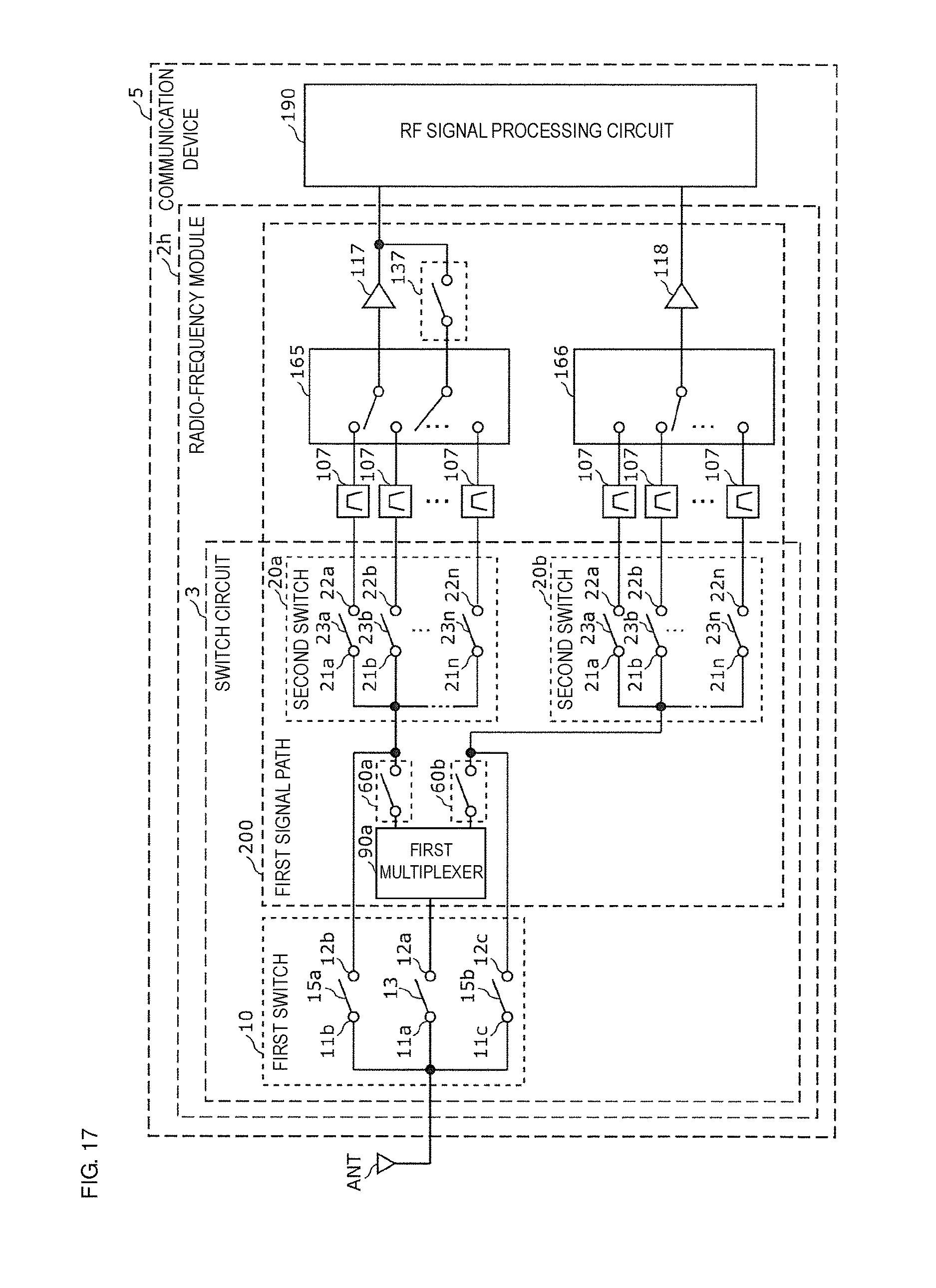
This application claims the benefit of priority to Japanese Patent Application No. 2017-103468 filed on May 25, 2017, Japanese Patent Application No. 2016-254538 filed on Dec. 27, 2016 and Japanese Patent Application No. 2016-158060 filed on Aug. 10, 2016. The entire contents of these applications are hereby incorporated herein by reference. The present invention relates to a switch circuit, a radio-frequency module, and a communication device. Lately, there has been an increasing demand for supporting a carrier aggregation (CA) for simultaneously sending and receiving multiple signals of different frequency bands. Japanese Unexamined Patent Application Publication No. 2015-115866 discloses a circuit using a quadplexer such as that shown in The known CA-support circuit 400 simultaneously sends and receives multiple signals of different frequency bands by using a quadplexer (multiplexer) 420 connected to an antenna 410. When a signal passes through a multiplexer, insertion loss occurs because of this multiplexer. For example, in the known CA-support circuit 400 shown in Accordingly, preferred embodiments of the present invention provide switch circuits, radio-frequency modules, and communication devices that are able to support CA communication and also to reduce insertion loss caused by a multiplexer when CA communication is not performed. According to a preferred embodiment of the present invention, a switch circuit includes first and second switches. The first switch includes a first common terminal and at least two first selection terminals selectively connected to the first common terminal. The second switch includes at least one second common terminal and at least one second selection terminal selectively connected to the at least one second common terminal. One of the at least two first selection terminals and the at least one second common terminal are connected to each other via a path passing through a first multiplexer. The first multiplexer is a filter which separates one signal into multiple signals of different frequency bands or integrates multiple signals of different frequency bands into one signal. Another one of the at least two first selection terminals and the at least one second common terminal are connected to each other via a bypass path bypassing the first multiplexer. With the above-described configuration, the first and second switches are connected to each other via at least two paths, that is, the path passing through the first multiplexer and the bypass path bypassing the first multiplexer. Connecting the first common terminal and a certain first selection terminal allows RF signals to pass through the first multiplexer, thus achieving CA communication. When CA communication is not performed, the first common terminal and another certain first selection terminal are connected to each other so as to allow RF signals to transmit between the first and second switches without passing through the first multiplexer. As a result, the switch circuit of the present preferred embodiment is able to support CA communication and also to reduce insertion loss caused by the multiplexer when CA communication is not performed. The at least one second selection terminal may include a second selection terminal connected to a terminating resistor. A high power signal received by an antenna may leak to the second switch even when the first common terminal and the at least two first selection terminals are not connected to each other. To address this issue, in the present preferred embodiment, a terminating resistor is connected to one of the at least one second selection terminal. By connecting the second common terminal and the second selection terminal to which the terminating resistor is connected, the terminating resistor is able to output energy of a high power signal received by the antenna to a ground. It is thus less likely that a circuit, such as a filter or a low-noise amplifier (LNA), connected to the second switch will be broken or the performance will be decreased by a high power signal. A matching circuit may be disposed between the at least two first selection terminals and the at least one second common terminal. The matching circuit performs impedance matching between the first and second switches, thus decreasing the level of loss (return loss) which may occur in an RF signal transmitted between the first and second switches. The second switch may include at least two second common terminals as the at least one second common terminal. The first selection terminal connected to the path passing through the first multiplexer and one of the at least two second common terminals may be connected to each other via the path passing through the first multiplexer. The first selection terminal connected to the bypass path bypassing the first multiplexer and another one of the at least two second common terminals may be connected to each other via the bypass path. The path passing through the first multiplexer and the bypass path bypassing the first multiplexer are connected to different second common terminals of the at least two second common terminals. Accordingly, the path passing through the first multiplexer and the bypass path bypassing the first multiplexer do not join together, thus making it possible to reduce insertion loss caused by the multiplexer when CA communication is not performed while enhancing the isolation between these paths. A path passing through a filter and a bypass path bypassing the filter may be connected to the at least one second selection terminal. The path passing through the filter and the bypass path bypassing the filter may be connected to different second selection terminals of the at least one second selection terminal. At least two paths, that is, the path passing through the filter and the bypass path bypassing the filter, are connected to the second switch. By connecting one of the at least two second common terminals and one certain second selection terminal with each other, an RF signal transmitted through the path connected to the second selection terminal passes through the filter, thus making it possible to filter this RF signal by using the filter. When filtering of this RF signal is not necessary, one of the at least two second common terminals and another certain second selection terminal are connected to each other, so that the RF signal is able to be transmitted to the path connected to this second selection terminal without passing through the filter. As a result, when filtering of an RF signal is not necessary, insertion loss caused by the filter is able to be reduced. A path passing through an amplifier circuit and a bypass path bypassing the amplifier circuit may directly or indirectly be connected to the at least one second selection terminal. The path passing through the amplifier circuit and the bypass path bypassing the amplifier circuit may be connected to different second selection terminals of the at least one second selection terminal. At least two paths, that is, the path passing through the amplifier circuit and the bypass path bypassing the amplifier circuit, are directly or indirectly connected to the second switch. When the path passing through the amplifier circuit and the bypass path bypassing the amplifier circuit are directly connected to the second switch, one of the at least two second common terminals and one certain second selection terminal are connected to each other. This allows an RF signal transmitted through the path connected to this second selection terminal to pass through the amplifier circuit, thus making it possible to amplify this RF signal. When amplifying of this RF signal is not necessary, one of the at least two second common terminals and another certain second selection terminal are connected to each other, so that the RF signal is able to be transmitted to the bypass path connected to this second selection terminal without passing through the amplifier circuit. When the path passing through the amplifier circuit and the bypass path bypassing the amplifier circuit are indirectly (via a different switch, for example) connected to the second switch, one certain selection terminal of the different switch and one of common terminals of this switch are connected to each other. This allows an RF signal transmitted through the path connected to this selection terminal to pass through the amplifier circuit, thus making it possible to amplify this RF signal. When amplifying of this RF signal is not necessary, another certain selection terminal of the different switch and another one of the common terminals are connected to each other, so that the RF signal is able to be transmitted to the bypass path connected to this selection terminal without passing through the amplifier circuit. As a result, when amplifying of an RF signal is not necessary, power is not consumed by the amplifier circuit. A branching path that branches into a path passing through an amplifier circuit and a bypass path bypassing the amplifier circuit may directly or indirectly be connected to the at least one second selection terminal. A bypass switch may be disposed on the bypass path bypassing the amplifier circuit to selectively pass or block a signal flowing through the bypass path. The above-described branching path is directly or indirectly connected to the second switch. When the branching path is directly connected to the second switch, by turning OFF the bypass switch (single-pole single-throw (SPST) switch) disposed on the bypass path, an RF signal transmitted to the path connected to the at least one second selection terminal passes through the amplifier circuit, thus making it possible to amplify the RF signal in the amplifier circuit. When amplifying of this RF signal is not necessary, the bypass switch is turned ON, thus allowing the RF signal to be transmitted to the path connected to the at least one second selection terminal without passing through the amplifier circuit. When the branching path is indirectly (via a different switch, for example) connected to the second switch, by turning OFF the bypass switch, an RF signal transmitted to the path connected to this different switch passes through the amplifier circuit, thus making it possible to amplify the RF signal in the amplifier circuit. When amplifying of this RF signal is not necessary, the bypass switch is turned ON, thus allowing the RF signal to be transmitted to the path connected to the different switch without passing through the amplifier circuit. As a result, when amplifying of an RF signal is not necessary, power is not consumed by the amplifier circuit. The switch circuit may further include a third switch including at least two third selection terminals and at least one third common terminal selectively connected to the at least two third selection terminals. A branching path that branches into a path passing through an amplifier circuit and a bypass path bypassing the amplifier circuit may be connected to the first multiplexer. The path passing through the amplifier circuit may be connected to one of the at least two third selection terminals. The bypass path bypassing the amplifier circuit may be connected to another one of the at least two third selection terminals. A bypass switch may be disposed on the bypass path bypassing the amplifier circuit to selectively pass or block a signal flowing through the bypass path. The first multiplexer and the third switch are connected to each other by at least two paths, that is, the path passing through the amplifier circuit and the bypass path bypassing the amplifier circuit. By turning OFF the bypass switch disposed on the bypass path, an RF signal transmitted between the first multiplexer and the third switch passes through the amplifier circuit, thus making it possible to amplify the RF signal in the amplifier circuit. When amplifying of this RF signal is not necessary, the bypass switch is turned ON, thus allowing the RF signal to be transmitted between the first multiplexer and the third switch without passing through the amplifier circuit. As a result, when amplifying of an RF signal is not necessary, power is not consumed by the amplifier circuit. A matching circuit may be disposed before a branching point of the branching path. Providing a switch and an amplifier circuit into one chip (semiconductor chip) reduces the size of a module on which the switch and the amplifier circuit are mounted. It may be necessary to adjust impedance matching between the amplifier circuit and a component connected to the amplifier circuit according to the environments where the module is used. Consequently, the matching circuit that performs such impedance matching is not usually provided in the same chip as that of the switch and the amplifier circuit. In the above-described preferred embodiment, the matching circuit is disposed before the branching point of the branching path. Thus, it is not necessary to provide terminals that connect the matching circuit to a chip other than the terminals that input and output RF signals, thus reducing the size of the chip. A matching circuit may be disposed between a branching point of the branching path and the amplifier circuit. If a matching circuit, which performs impedance matching between the amplifier circuit and a component connected to the amplifier circuit, is disposed before the branching point of the branching path, an RF signal which will pass through the bypass path bypassing the amplifier circuit passes through the matching circuit. In this case, the frequency band of this RF signal may deviate from a desirable band as a result of passing through the matching circuit. In the above-described preferred embodiment, the matching circuit is disposed between the branching point of the branching path and the amplifier circuit. Thus, an RF signal which passes through the path passing through the amplifier circuit passes through the matching circuit and is thus subjected to impedance matching by the matching circuit. An RF signal which passes through the bypass path bypassing the amplifier circuit does not pass through the matching circuit and is not subjected to impedance matching. The first switch may include at least three first selection terminals as the at least two first selection terminals. Among the at least three first selection terminals, a first selection terminal other than the first selection terminal connected to the path passing through the first multiplexer and the first selection terminal connected to the bypass path bypassing the first multiplexer may be a sending first selection terminal. When the first common terminal of the first switch is connected to the first selection terminal connected to the path passing through the first multiplexer or the first selection terminal connected to the bypass path bypassing the first multiplexer, the antenna is able to be used as a receive antenna. When the first common terminal is connected to the sending first selection terminal, the antenna is able to be used as a transmit antenna. Thus, the antenna is able to be used as a transmit-and-receive antenna, thus reducing the size of a communication device, such as a cellular phone. The switch circuit may include two or more second switches as the second switch. The first common terminal may be connected to an antenna. The at least two first selection terminals may be each connected to a first signal path. The two or more second switches may be disposed in the first signal path and may each include one second common terminal as the at least one second common terminal. The first selection terminal connected to the path passing through the first multiplexer may be connected to the second common terminal via the path passing through the first multiplexer. The first selection terminal connected to the bypass path bypassing the first multiplexer may be connected to the second common terminal via the bypass path. A fourth switch may be disposed between the first multiplexer and the second common terminal. A signal received by the antenna may be transmitted to the first signal path via the first multiplexer when the first common terminal and the first selection terminal connected to the path passing through the first multiplexer are connected to each other and when the fourth switch is ON. A signal received by the antenna may be transmitted to the first signal path without passing through the first multiplexer when the first common terminal and the first selection terminal connected to the bypass path bypassing the first multiplexer are connected to each other and when the fourth switch is OFF. By connecting the first common terminal and the first selection terminal connected to the bypass path bypassing the first multiplexer to each other and by turning OFF the fourth switch, a signal received by the antenna is able to be transmitted to the first signal path without passing through the first multiplexer. When CA communication is performed, the first common terminal and the first selection terminal connected to the path passing through the first multiplexer are connected to each other, and the fourth switch 60 is turned ON. In contrast, when CA communication is not performed, the first common terminal and the first selection terminal connected to the bypass path bypassing the first multiplexer are connected to each other, and the fourth switch is turned OFF. It is thus possible to support CA communication and also to reduce insertion loss caused by the first multiplexer when CA communication is not performed. The first switch may include at least three first selection terminals as the at least two first selection terminals. Among the at least three first selection terminals, at least one first selection terminal other than the first selection terminal connected to the path passing through the first multiplexer and the first selection terminal connected to the bypass path bypassing the first multiplexer may be at least one sending first selection terminal. The at least one sending first selection terminal may be connected to a second signal path, which is a path different from the first signal path. A signal to be sent from the antenna may be transmitted to the second signal path when the first common terminal and the at least one sending first selection terminal are connected to each other. When the first common terminal is connected to the first selection terminal connected to the path passing through the first multiplexer or the first selection terminal connected to the bypass path bypassing the first multiplexer, the single antenna is able to be used as a receive antenna, thus enabling the switch circuit to receive signals of different frequency bands received by the antenna. When the first common terminal is connected to the sending first selection terminal, a sending signal transmitted to the second signal path is able to be sent to the single antenna, and the antenna can also be used as a transmit antenna. By using the switch circuit that is able to receive signals of different frequency bands, the single antenna may be used as a transmit-and-receive antenna, thus reducing the size of a communication device, such as a cellular phone. The switch circuit may further include a fifth switch. The fifth switch is disposed in the second signal path and includes a fifth common terminal connected to the at least one sending first selection terminal and includes at least two fifth selection terminals. The fifth switch makes it possible to simultaneously send multiple sending signals of different frequency bands. A matching circuit may be disposed between the at least one sending first selection terminal and the fifth common terminal. The matching circuit performs impedance matching between the first switch and the fifth switch, thus decreasing the level of loss (return loss) which may occur in a signal transmitted to the second signal path. The switch circuit may include two or more fifth switches as the fifth switch. A second multiplexer may be connected between one of the at least one sending first selection terminal and the fifth common terminal of each of the two or more fifth switches. This makes it possible to simultaneously send multiple sending signals of different frequency bands, thus achieving CA communication for sending signals. The first switch may include at least two sending first selection terminals as the at least one sending first selection terminal. A sixth switch may be connected between the second multiplexer and the fifth common terminal. A signal to be sent from the antenna may be transmitted to the second signal path without passing through the second multiplexer when the first common terminal and another one of the at least two sending first selection terminals are connected to each other and when the sixth switch is OFF. By connecting the first common terminal and another one of the at least two sending first selection terminals to each other and by turning OFF the sixth switch, a signal transmitted to the second signal path can be sent to the antenna without passing through the second multiplexer. As a result, when CA communication is not performed, insertion loss caused by the multiplexer is able to be reduced. According to another preferred embodiment of the present invention, a radio-frequency module includes the above-described switch circuit, a filter connected to the at least one second selection terminal, and an amplifier circuit connected to the filter. It is thus possible to provide a radio-frequency module that is able to support CA communication and also to reduce insertion loss caused by a multiplexer when CA communication is not performed. According to another preferred embodiment of the present invention, a communication device includes a radio-frequency signal processing circuit and the above-described radio-frequency module. The radio-frequency signal processing circuit processes a radio-frequency signal sent or received by an antenna. The above-described radio-frequency module transmits the radio-frequency signal between the antenna and the radio-frequency signal processing circuit. It is thus possible to provide a communication device that is able to support CA communication and also to reduce insertion loss caused by a multiplexer when CA communication is not performed. According to preferred embodiments of the present invention, it is possible to provide switch circuits, radio-frequency modules, and communication devices that are able to support CA communication and also to reduce insertion loss caused by a multiplexer when CA communication is not performed. The above and other elements, features, steps, characteristics and advantages of the present invention will become more apparent from the following detailed description of the preferred embodiments with reference to the attached drawings. Preferred embodiments of the present invention will be described below in detail with reference to the accompanying drawings. All of the preferred embodiments described below illustrate general or specific examples. Numeric values, components, and positions and connection states of the components illustrated in the following preferred embodiments are only examples, and are not described for limiting the present invention. Among the components illustrated in the following preferred embodiments, the components that are not recited in the independent claims which embody the broadest concept of various preferred embodiments of the present invention will be described as optional components. The drawings are only schematic drawings and do not necessarily illustrate the components precisely. In the drawings, the same components are designated by like reference numerals. A switch circuit 1 according to a first preferred embodiment of the present invention will be described below with reference to The antenna ANT is a multiband-support antenna which sends and receives radio-frequency (RF) signals in compliance with a communication standard, such as Long Term Evolution (LTE). The antenna ANT may be a main antenna. The antenna ANT may alternatively be a sub antenna (diversity antenna) separately provided from a main antenna to improve the quality and the reliability of communication. The switch circuit 1 supports carrier aggregation (CA) in which at least two different frequency bands are simultaneously used. The switch circuit 1 is disposed in a front-end portion of a communication device, such as a cellular phone, for example. In the first preferred embodiment, the switch circuit 1 is connected to the antenna ANT. The switch circuit 1 includes a first switch 10, a second switch 20, and a first multiplexer 90 The first switch 10 includes a first common terminal 11 and at least two first selection terminals 12 selectively connected to the first common terminal 11. In the first preferred embodiment, the first switch 10 includes two first selection terminals 12 One of the first selection terminals 12 The second switch 20 includes at least one second common terminal and at least one second selection terminal selectively connected to the at least one second common terminal. In the first preferred embodiment, the second switch 20 includes at least two second common terminals (more specifically, two second common terminals 21 One of the at least two first selection terminals of the first switch 10 and one of the at least two second common terminals of the second switch 20 are connected to each other via a path passing through the first multiplexer 90 Another one of the at least two first selection terminals of the first switch 10 and another one of the at least two second common terminals of the second switch 20 are connected to each other via a bypass path 202 bypassing the first multiplexer 90 The multiplexer includes filters which separate one signal into multiple signals of different frequency bands or integrate multiple signals of different frequency bands into one signal. The multiplexer includes plural filters. A terminal at one end of each filter is connected to a terminal at the same end of another filter, thus integrating the plural filters into each other. That is, the multiplexer is a duplexer, a triplexer, or a quadplexer. The first multiplexer 90 Each of the filters of the first multiplexer 90 The filters of the first multiplexer 90 When an RF signal passes through a multiplexer, insertion loss occurs because of this multiplexer. In the CA-support circuit 400 shown in In contrast, in the first preferred embodiment, at least two paths are provided to connect the first switch 10 and the second switch 20. One path is a combination of the paths 201 and 201 The path passing through the first multiplexer 90 A radio-frequency module 2 The radio-frequency module 2 The switch circuit according to the second preferred embodiment includes a switch 30 in addition to the elements of the switch circuit 1 of the first preferred embodiment. The switch 30 includes at least two selection terminals and at least one common terminal selectively connected to the at least two selection terminals. In the second preferred embodiment, the switch 30 includes three selection terminals 32 A path passing through a filter and a bypass path bypassing the filter are connected to at least one second selection terminal (at least two second selection terminals in the second preferred embodiment) of the second switch 20. The path passing through a filter and the bypass path bypassing the filter are connected to different second selection terminals. More specifically, one of the at least two second selection terminals of the second switch 20 and one of the at least two selection terminals of the switch 30 are connected to each other via a path passing through a filter. Plural second selection terminals of the second switch 20 and the associating plural selection terminals of the switch 30 may be connected to each other via paths passing through filters. In Another one of the at least two second selection terminals of the second switch 20 and another one of the at least two selection terminals of the switch 30 are connected to each other via a bypass path 205 bypassing the filters 101 and 102. In Each of the filters 101 and 102 is a band pass filter which allows signals of a predetermined frequency band to pass therethrough. The filters 101 and 102 each include a SAW resonator, a BAW resonator, or a film bulk acoustic resonator (FBAR). A SAW filter may include IDT electrodes on a piezoelectric substrate. Accordingly, if the filters 101 and 102 are SAW filters including SAW resonators, they can be small and thin and also exhibit sharp bandpass characteristics. The filters 101 and 102 may alternatively be LC resonance circuits including circuit elements, such as inductors and capacitors. The piezoelectric substrate preferably has piezoelectricity at least on its surface. For example, the piezoelectric substrate may include a piezoelectric thin film on its surface, and may be a multilayer body including the piezoelectric thin film and another film having different acoustic velocities, and a support substrate. Alternatively, the entirety of the piezoelectric substrate may have piezoelectricity. In this case, the piezoelectric substrate includes a single piezoelectric layer. An RF signal received by the second common terminal 21 To address this issue, in the second preferred embodiment, at least two paths, that is, the path (path 203 or 204) passing through the filter (filter 101 or 102) and the bypass path 205 bypassing the filters, are connected to the second switch 20. By connecting one of the at least two second common terminals and the second selection terminal 22 A radio-frequency module 2 A path 206 passing through the amplifier circuit 111 and a bypass path 207 bypassing the amplifier circuit 111 are directly connected to at least one second selection terminal (at least two selection terminals in the third preferred embodiment) of the second switch 20. The path 206 passing through the amplifier circuit 111 and the bypass path 207 bypassing the amplifier circuit 111 are connected to different second selection terminals. More specifically, one of the at least two second selection terminals of the second switch 20 and one of the at least two selection terminals of the switch 30 are connected to each other via the path 206 passing through the amplifier circuit 111. In Another one of the at least two second selection terminals of the second switch 20 and another one of the at least two selection terminals of the switch 30 are connected to each other via the bypass path 207 bypassing the amplifier circuit 111. In The amplifier circuit 111 is a circuit that amplifies RF signals. The amplifier circuit 111 is a low-noise amplifier (LNA) that amplifies RF received signals or a power amplifier that amplifies RF sending signals. The matching circuit 121 is a circuit that performs impedance matching between the amplifier circuit 111 and the second switch 20. The matching circuit 121 is disposed between the second selection terminal 22 An RF signal received by the second common terminal 21 To address this issue, in the third preferred embodiment, at least two paths, that is, the path 206 passing through the amplifier circuit 111 and the bypass path 207 bypassing the amplifier circuit 111, are directly connected to the second switch 20. By connecting one of the at least two second common terminals and the second selection terminal 22 In the third preferred embodiment, the path 206 passing through the amplifier circuit 111 and the bypass path 207 bypassing the amplifier circuit 111 are separate paths connected to different terminals. However, the path 206 and the bypass path 207 may branch off from one path. A path 208 which branches into a path 208 More specifically, the path 208 which branches into the path 208 The matching circuit 121 is disposed after the branching point x1, and more specifically, between the branching point x1 and the amplifier circuit 111 on the path 208 An RF signal received by the second common terminal 21 To address this issue, in this modified example, the path 208 which branches into at least two paths, that is, the path 208 A radio-frequency module 2 The switch 40 includes at least two selection terminals and at least one common terminal selectively connected to the at least two selection terminals. In the fourth preferred embodiment, the switch 40 includes two selection terminals 42 A path 209 passing through the amplifier circuit 112 and a bypass path 210 bypassing the amplifier circuit 112 are indirectly connected to at least one second selection terminal (at least two selection terminals in the fourth preferred embodiment) of the second switch 20. Indirectly connecting the path 209 and the bypass path 210 to the at least one second selection terminal means that the path 209 and the bypass path 210 are connected to the at least one second selection terminal via another component (switch 30, for example). The path 209 passing through the amplifier circuit 112 and the bypass path 210 bypassing the amplifier circuit 112 are connected to different second selection terminals. More specifically, one of the at least two common terminals of the switch 30 and one of the at least two selection terminals of the switch 40 are connected to each other via the path 209 passing through the amplifier circuit 112. In Another one of the at least two common terminals of the switch 30 and another one of the at least two selection terminals of the switch 40 are connected to each other via the bypass path 210 bypassing the amplifier circuit 112. In The matching circuit 122 is a circuit that performs impedance matching between the amplifier circuit 112 and the switch 30. The matching circuit 122 is disposed between the common terminal 31 An RF signal received by one of the selection terminals 32 To address this issue, in the fourth preferred embodiment, at least two paths, that is, the path 209 passing through the amplifier circuit 112 and the bypass path 210 bypassing the amplifier circuit 112, are indirectly (via the switch 30, for example) connected to the second switch 20. That is, at least two paths, that is, the path 209 passing through the amplifier circuit 112 and the bypass path 210 bypassing the amplifier circuit 112 are connected to the switch 30. By connecting one of the at least two selection terminals of the switch 30 and the common terminal 31 In the fourth preferred embodiment, the path 209 passing through the amplifier circuit 112 and the bypass path 210 bypassing the amplifier circuit 112 are separate paths connected to different terminals. However, the path 209 and the bypass path 210 may branch off from one path. A path 211 which branches into a path 211 More specifically, the path 211 which branches into the path 211 The matching circuit 122 is disposed after the branching point x2, and more specifically, between the branching point x2 and the amplifier circuit 112 on the path 211 An RF signal received by one of the selection terminals 32 To address this issue, in this modified example, the path 211 which branches into at least two paths, that is, the path 211 A radio-frequency module 2 The radio-frequency module 2 The third switch 50 includes at least two third selection terminals and at least one third common terminal selectively connected to the at least two third selection terminals. In the fifth preferred embodiment, the third switch 50 includes two third selection terminals 52 The path 212 which branches into a path 212 The matching circuit 123 is disposed after the branching point x3, and more specifically, between the branching point x3 and the amplifier circuit 113 on the path 212 An RF signal propagating through the path 212 is amplified as a result of passing through the amplifier circuit 113. However, when an RF signal passes through an amplifier circuit, power is consumed because of the amplification of the amplifier circuit. This leads to a waste of power if an RF signal which is not required to be amplified passes through the amplifier circuit. To address this issue, in the fifth preferred embodiment, the first multiplexer 90 In the modified examples of the third and fourth preferred embodiments and the fifth preferred embodiment, the matching circuit is disposed after the branching point. However, the matching circuit may be disposed before the branching point. A description will now be given of the radio-frequency module 2 Providing a switch and an amplifier circuit into one chip (semiconductor chip) reduces the size of a module on which the switch and the amplifier circuit are mounted. For example, the third switch 50, the bypass switch 133, and the amplifier circuit 113 may be provided in and defined by one chip. It may however be necessary to adjust impedance matching between the amplifier circuit 113 and a component connected to the amplifier circuit 113 (first multiplexer 90 Typically, as shown in In contrast, as shown in Typically, if a matching circuit, which performs impedance matching between an amplifier circuit and a component connected to the amplifier circuit, is disposed before a branching point of a path, an RF signal which will pass through a bypass path bypassing the amplifier circuit passes through the matching circuit. In this case, the frequency band of this RF signal may deviate from a desirable band as a result of passing through the matching circuit. In contrast, in the fifth preferred embodiment, as shown in In the radio-frequency modules 2 The first switch 10 The paths 201 The path 214 is connected to a common terminal of a switch 161, and filters 103 and 104 are connected to two selection terminals of the switch 161. The path 215 is connected to a common terminal of a switch 162, and filters 105 and 106 are connected to two selection terminals of the switch 162. The filters 101 and 102 have different HB frequency bands as the pass bands. The filters 103 and 104 have different MHB frequency bands as the pass bands. The filters 105 and 106 have different LMB frequency bands as the pass bands. The filters 103 and 104 are connected to two selection terminals of a switch 163. A path that branches into a path passing through an amplifier circuit 114 and a bypass path bypassing the amplifier circuit 114 is connected to a common terminal of the switch 163. A bypass switch 134 is provided on the bypass path bypassing the amplifier circuit 114. A matching circuit 124 is disposed before a branching point of this path to perform impedance matching between the switch 163 and the amplifier circuit 114. A path that branches into a path passing through an amplifier circuit 115 and a bypass path bypassing the amplifier circuit 115 is connected to the filter 105. A bypass switch 135 is provided on the bypass path bypassing the amplifier circuit 115. A matching circuit 125 is disposed between a branching point of this path and the amplifier circuit 115 to perform impedance matching between the filter 105 and the amplifier circuit 115. A path that branches into a path passing through an amplifier circuit 116 and a bypass path bypassing the amplifier circuit 116 is connected to the filter 106. A bypass switch 136 is provided on the bypass path bypassing the amplifier circuit 116. A matching circuit 126 is disposed before a branching point of this path to perform impedance matching between the filter 106 and the amplifier circuit 116. The paths passing through the amplifier circuits 114 through 116 are connected to one of two selection terminals of a switch 164, while the bypass paths bypassing the amplifier circuits 114 through 116 are connected to the other one of the two selection terminals of the switch 164. A band select switch 170 is connected to a common terminal of the switch 164. That is, the switch 164 selects one of an RF received signal (LMB or MHB RF received signal) amplified by a corresponding one of the amplifier circuits 114 through 116 and an RF received signal that has not been amplified by a corresponding one of the amplifier circuits 114 through 116, and supplies the selected RF received signal to the band select switch 170. The band select switch 170 is connected to the common terminal 41 of the switch 40. The switch 40 selects one of an RF received signal (HB RF received signal or RF received signal which has not passed through the first multiplexer 90 The band select switch 170 is connected to the third common terminal 51 of the third switch 50. The third switch 50 selects one of an RF received signal (MB RF received signal) amplified by the amplifier circuit 113 and an RF received signal that has not been amplified by the amplifier circuit 113, and supplies the selected RF received signal to the band select switch 170. The band select switch 170 is connected to an RF signal processing circuit (not shown), for example, and assigns multiple RF received signals of different frequency bands to associated terminals of the RF signal processing circuit. When the antenna ANT is used to send RF signals, the band select switch 170 connects the RF signal processing circuit and the bypass path 213. An explanation of details of the band select switch 170 will be omitted. In the sixth preferred embodiment, the sending first selection terminal 16 In the sixth preferred embodiment, when the first common terminal 11 of the first switch 10 A switch circuit 3 according to a seventh preferred embodiment of the present invention will be described below with reference to The switch circuit 3 is a circuit that can receive signals of different frequency bands received by the antenna ANT. That is, the switch circuit 3 is a CA-support switch. The switch circuit 3 includes a first switch 10 The first switch 10 The switches 13 and 15 are semiconductor switches such as diode switches or FET switches, and are turned ON or OFF in accordance with a control signal from an external source (RF signal processing circuit, for example) outside the first switch 10 The second switch 20 includes at least one second common terminal 21 connected to the first selection terminals 12 The switch 23 is a semiconductor switch such as a diode switch or an FET switch, and is turned ON or OFF in accordance with a control signal from an external source (RF signal processing circuit, for example) outside the second switch 20. The second common terminals 21 The second switch 20 is disposed on the first signal path 200. This means that the second switch 20 is disposed on a path connected to the first selection terminals 12 A signal received by the antenna ANT passes through the first signal path 200 when the first common terminal 11 and at least one of the first selection terminals 12 The first selection terminal 12 The first selection terminal 12 A fourth switch 60 The fourth switch 60 is a semiconductor switch such as a diode switch or an FET switch, and is turned ON or OFF in accordance with a control signal from an external source (RF signal processing circuit, for example) outside the switch circuit 3. By using the first multiplexer 90 To address this issue, in the seventh preferred embodiment, the switch circuit 3 preferably has the following structure. A signal received by the antenna ANT is transmitted to the first signal path 200 via the first multiplexer 90 This will be explained more specifically. When the first common terminal 11 With the above-described configuration, when CA communication is not performed, insertion loss which may occur in a received signal is reduced. The switch circuit 3 is able to support CA communication and also to reduce insertion loss caused by the first multiplexer 90 A switch circuit 3 The switch circuit 3 The terminating resistor 160 is connected to one of at least two second selection terminals 22 of the second switch 20 A high power signal received by the antenna ANT may leak to the second switch 20 A switch circuit 3 The switch circuit 3 The matching circuit 180 As described above, filters having different pass bands from each other are connected to the at least two second selection terminals 22 of each of the second switches 20 As described above, the impedance matching parameter or the connection mode of the matching circuit 180 is adjusted in advance to the frequency band to be subjected to impedance matching, or is changed in accordance with a control signal for turning ON or OFF the switch 23 received by the second switch 20 A switch circuit 3 The switch circuit 3 The sending first selection terminal 16 The switch 17 is a semiconductor switch such as a diode switch or an FET switch, and is turned ON or OFF in accordance with a control signal from an external source (RF signal processing circuit, for example) outside the first switch 10 The fifth switch 70 includes a fifth common terminal 71 connected to the sending first selection terminal 16 The fifth switch 70 is disposed on the second signal path 300. This means that the fifth switch 70 is disposed on a path connected to the sending first selection terminal 16 A signal to be sent from the antenna ANT is transmitted to the second signal path 300 when the first common terminal 11 As shown in By using the switch circuit 3 In this case, even when the first common terminal 11 and the first selection terminals 12 A switch circuit 3 The switch circuit 3 The second multiplexer 90 The filters of the second multiplexer 90 The first switch 10 The sixth switch 80 By turning ON the switch 13 and the fourth switches 60 When the switch 13 is ON, the switches 15 The second multiplexer 90 To address this issue, in the eleventh preferred embodiment, when the first common terminal 11 and a sending first selection terminal (sending first selection terminal 16 The matching circuit 180 As described above, filters having different pass bands from each other are connected to the at least two fifth selection terminals 72 of the fifth switch 70. That is, the frequency band for which the matching circuit 180 performs impedance matching differs depending on which switch 73 will be turned ON. The matching circuit 180 predicts which switch 73 in the fifth switch 70 will be turned ON and adjusts itself in advance to the frequency band of a signal to be subjected to impedance matching. If the parameter used to perform impedance matching in the matching circuit 180 is variable, a control signal used to turn ON or OFF the switch 73 received by the second switch 70 is also received by the matching circuit 180 (matching circuits 180 As described above, the impedance matching parameter or the connection mode of the matching circuit 180 is adjusted in advance to the frequency band to be subjected to impedance matching, or is changed in accordance with a control signal for turning ON or OFF the switch 73 received by the fifth switch 70. It is thus possible to achieve significantly improved or optimal impedance matching according to the frequency band. A switch circuit and a radio-frequency module according to a preferred embodiment of the present invention is applicable to a communication device. In a twelfth preferred embodiment of the present invention, a communication device 4 including a switch circuit (radio-frequency module) will be described. The communication device 4 includes the radio-frequency module 2 The radio-frequency module 2 The RF signal processing circuit 190 is a circuit that processes the RF signal. The RF signal processing circuit 190 performs signal processing, such as down-conversion, on a received signal input from the antenna ANT and outputs the resulting received signal to a baseband signal processing circuit (not shown). The RF signal processing circuit 190 also performs signal processing, such as up-conversion, on a sending signal input from the baseband signal processing circuit and outputs the resulting sending signal to the antenna ANT. A communication device 5 including a switch circuit (radio-frequency module) will be described below as a modified example of the twelfth preferred embodiment. The communication device 5 includes a radio-frequency module 2 The radio-frequency module 2 The filters 107 are filters including elastic wave resonators or LC circuits. The filters 107 may be band pass filters. Other examples of the filters 107 are a high pass filter, a low pass filter, and a band elimination filter. The filters 107 have different pass bands from each other. The filters 107 are connected to the second selection terminal 22, so that the switch circuit 3 is able to receive signals of different frequency bands. The pass bands of the filters 107 are in a range of about 700 MHz to about 3.5 GHz, for example. The switches 165 and 166 include plural selection terminals connected to the filters 107, common terminals connected to the amplifier circuits 117 and 118, and a common terminal connected to the bypass switch 137. The switches 165 and 166 each select one of the common terminals and one of the selection terminals in accordance with a control signal output from the RF signal processing circuit 190, for example. The switch 165 selects the selection terminal connected to the filter 107 associated with a desired frequency band and the common terminal connected to the amplifier circuit 117 or the bypass switch 137. The switch 166 selects the selection terminal connected to the filter 107 associated with a desired frequency band and the common terminal connected to the amplifier circuit 118. The amplifier circuits 117 and 118 are LNAs that amplify RF received signals and output them to the RF signal processing circuit 190. The bypass switch 137 is turned ON when amplifying of an RF received signal is not necessary. When the bypass switch 137 is ON, the selection terminal connected to the filter 107 is connected to the common terminal connected to the bypass switch 137 instead of that connected to the amplifier circuit 117. The RF signal processing circuit 190 is a circuit that processes an RF signal received by the antenna ANT. The RF signal processing circuit 190 performs signal processing, such as down-conversion, on an RF received signal input from the antenna ANT via the first signal path 200 and outputs the resulting received signal to a baseband signal processing circuit (not shown). The radio-frequency module 2 As described above, the switch circuit or the radio-frequency module according to a preferred embodiment of the present invention may be applied to a communication device. The switch circuits, radio-frequency modules, and communication devices according to the preferred embodiments have been discussed. However, the present invention is not restricted to the above-described preferred embodiments. In the above-described preferred embodiments, the switch circuit includes at least one of the first and second multiplexers 90 In the above-described preferred embodiments, the first switch 10 through the third switch 50 are n-pole n-throw (nPnT) (n≧1) switches. However, the first switch 10 through the third switch 50 may be another type of switch. For example, the first switch 10 through the third switch 50 may be formed as a combination of SPST switches, as in the first switch 10 Although in the first through seventh preferred embodiments, the second switch 20 does not include a terminating resistor 160, it may include a terminating resistor 160. That is, in the first through seventh preferred embodiments, the terminating resistor 160 may be connected to at least one of the second selection terminals. Although in the first through eighth preferred embodiments, a matching circuit 180 is not disposed between the first switch 10 and the second switch 20, a matching circuit 180 may be disposed therebetween. That is, in the first through eighth preferred embodiments, matching circuits 180 may be disposed between the at least two first selection terminals of the first switch 10 and the at least one second common terminal of the second switch 20. In the eighth through eleventh preferred embodiments, the terminating resistors 160 are built in the second switches 20 In the eighth through eleventh preferred embodiments, the switch circuit includes the second switches 20 In the ninth preferred embodiment, the matching circuit 180 is connected between the first selection terminal 12 In the tenth preferred embodiment, the matching circuit 180 is connected between the first selection terminal 12 Although in the tenth preferred embodiment the matching circuit 180 is not connected between the sending first selection terminal 16 In the eleventh preferred embodiment, the matching circuit 180 is connected all of between the first selection terminal 12 Although in the seventh through tenth preferred embodiments, the switch circuit includes two second switches, it may include three or more second switches. Although in the eleventh preferred embodiment, the switch circuit 3 Preferred embodiments obtained by making various modifications to the above-described preferred embodiments by those skilled in the art and preferred embodiments achieved by combining the elements and functions of the above-described preferred embodiments without departing from the scope and spirit of the invention are also encompassed in the present invention. Preferred embodiments of the present invention are widely applicable in communication devices, such as cellular phones, as switch circuits, radio-frequency modules, and communication devices that are able to support CA communication and also to reduce insertion loss caused by a multiplexer when CA communication is not performed. While preferred embodiments of the present invention have been described above, it is to be understood that variations and modifications will be apparent to those skilled in the art without departing from the scope and spirit of the present invention. The scope of the present invention, therefore, is to be determined solely by the following claims. A switch circuit includes first and second switches. The first switch includes a first common terminal and at least two first selection terminals selectively connected to the first common terminal. The second switch includes at least one second common terminal and at least one second selection terminal selectively connected to the at least one second common terminal. One of the at least two first selection terminals and the at least one second common terminal are connected to each other via a path passing through a first multiplexer. Another one of the at least two first selection terminals and the at least one second common terminal are connected to each other via a bypass path bypassing the first multiplexer. 1. A switch circuit comprising:
a first switch including a first common terminal and at least two first selection terminals selectively connected to the first common terminal; and a second switch including at least one second common terminal and at least one second selection terminal selectively connected to the at least one second common terminal; wherein one of the at least two first selection terminals and the at least one second common terminal are connected to each other via a path passing through a first multiplexer, the first multiplexer being a filter that separates one signal into a plurality of signals of different frequency bands or integrates a plurality of signals of different frequency bands into one signal; and another one of the at least two first selection terminals and the at least one second common terminal are connected to each other via a bypass path bypassing the first multiplexer. 2. The switch circuit according to 3. The switch circuit according to 4. The switch circuit according to the second switch includes at least two second common terminals defining the at least one second common terminal; the first selection terminal connected to the path passing through the first multiplexer is connected to one of the at least two second common terminals via the path passing through the first multiplexer; and the first selection terminal connected to the bypass path bypassing the first multiplexer is connected to another one of the at least two second common terminals via the bypass path. 5. The switch circuit according to a path passing through a filter and a bypass path bypassing the filter are connected to the at least one second selection terminal; and the path passing through the filter and the bypass path bypassing the filter are connected to different second selection terminals of the at least one second selection terminal. 6. The switch circuit according to a path passing through an amplifier circuit and a bypass path bypassing the amplifier circuit are directly or indirectly connected to the at least one second selection terminal; and the path passing through the amplifier circuit and the bypass path bypassing the amplifier circuit are connected to different second selection terminals of the at least one second selection terminal. 7. The switch circuit according to a branching path that branches into a path passing through an amplifier circuit and a bypass path bypassing the amplifier circuit is directly or indirectly connected to the at least one second selection terminal; and a bypass switch is disposed on the bypass path bypassing the amplifier circuit to selectively pass or block a signal flowing through the bypass path. 8. The switch circuit according to a third switch including at least two third selection terminals and at least one third common terminal selectively connected to the at least two third selection terminals; wherein a branching path that branches into a path passing through an amplifier circuit and a bypass path bypassing the amplifier circuit is connected to the first multiplexer; the path passing through the amplifier circuit is connected to one of the at least two third selection terminals; the bypass path bypassing the amplifier circuit is connected to another one of the at least two third selection terminals; and a bypass switch is disposed on the bypass path bypassing the amplifier circuit to selectively pass or block a signal flowing through the bypass path. 9. The switch circuit according to 10. The switch circuit according to 11. The switch circuit according to the first switch includes at least three first selection terminals defining the at least two first selection terminals; and among the at least three first selection terminals, a first selection terminal other than the first selection terminal connected to the path passing through the first multiplexer and the first selection terminal connected to the bypass path bypassing the first multiplexer is a sending first selection terminal. 12. The switch circuit according to the switch circuit includes two or more second switches defining the second switch; the first common terminal is connected to an antenna; the at least two first selection terminals are each connected to a first signal path; the two or more second switches are disposed in the first signal path and each include one second common terminal defining the at least one second common terminal; the first selection terminal connected to the path passing through the first multiplexer is connected to the second common terminal via the path passing through the first multiplexer; the first selection terminal connected to the bypass path bypassing the first multiplexer is connected to the second common terminal via the bypass path; a fourth switch is disposed between the first multiplexer and the second common terminal; and a signal received by the antenna is transmitted to the first signal path via the first multiplexer when the first common terminal and the first selection terminal connected to the path passing through the first multiplexer are connected to each other and when the fourth switch is ON, and a signal received by the antenna is transmitted to the first signal path without passing through the first multiplexer when the first common terminal and the first selection terminal connected to the bypass path bypassing the first multiplexer are connected to each other and when the fourth switch is OFF. 13. The switch circuit according to the first switch includes at least three first selection terminals defining the at least two first selection terminals; among the at least three first selection terminals, at least one first selection terminal other than the first selection terminal connected to the path passing through the first multiplexer and the first selection terminal connected to the bypass path bypassing the first multiplexer is at least one sending first selection terminal; the at least one sending first selection terminal is connected to a second signal path, the second signal path being a path different from the first signal path; and a signal to be sent from the antenna is transmitted to the second signal path when the first common terminal and the at least one sending first selection terminal are connected to each other. 14. The switch circuit according to a fifth switch that is disposed in the second signal path and that includes a fifth common terminal connected to the at least one sending first selection terminal and includes at least two fifth selection terminals. 15. The switch circuit according to 16. The switch circuit according to the switch circuit includes two or more fifth switches defining the fifth switch; and a second multiplexer is connected between one of the at least one sending first selection terminal and the fifth common terminal of each of the two or more fifth switches. 17. The switch circuit according to the first switch includes at least two sending first selection terminals defining the at least one sending first selection terminal; a sixth switch is connected between the second multiplexer and the fifth common terminal; and a signal to be sent from the antenna is transmitted to the second signal path without passing through the second multiplexer when the first common terminal and another one of the at least two sending first selection terminals are connected to each other and when the sixth switch is OFF. 18. A radio-frequency module comprising:
the switch circuit according to a filter connected to the at least one second selection terminal; and an amplifier circuit connected to the filter. 19. A communication device comprising:
a radio-frequency signal processing circuit that processes a radio-frequency signal sent or received by an antenna; and the frequency module according to CROSS REFERENCE TO RELATED APPLICATIONS
BACKGROUND OF THE INVENTION
1. Field of the Invention
2. Description of the Related Art
SUMMARY OF THE INVENTION
BRIEF DESCRIPTION OF THE DRAWINGS
DETAILED DESCRIPTION OF THE PREFERRED EMBODIMENTS
First Preferred Embodiment
Second Preferred Embodiment
Third Preferred Embodiment
Fourth Preferred Embodiment
Fifth Preferred Embodiment
Sixth Preferred Embodiment
Seventh Preferred Embodiment
Eighth Preferred Embodiment
Ninth Preferred Embodiment
Tenth Preferred Embodiment
Eleventh Preferred Embodiment
Twelfth Preferred Embodiment
Other Preferred Embodiments