ELECTRIC POWER CONVERSION DEVICE
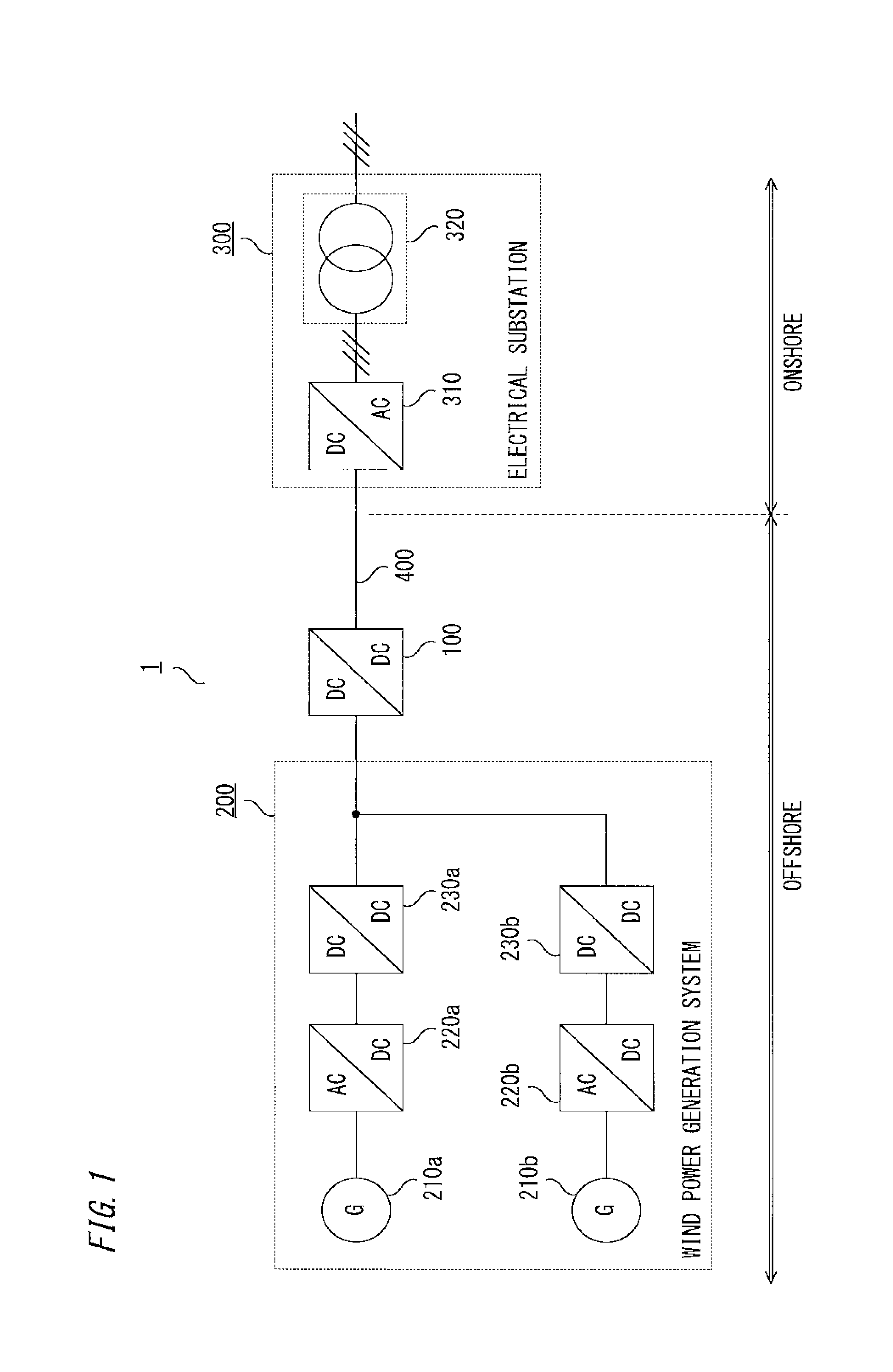
The present invention relates to a power conversion device that converts DC power to DC power having different voltage, and in particular, relates to a power conversion device used for high-voltage DC power transmission. In recent years, in offshore wind power generation, the amount of electric generation has been increasing with size increase in windmills, and the distance between a substation facility and windmills installed offshore has become further long. Powers generated by a plurality of electric generators are collected and transmitted to a substation facility. In order to cope with increase in the amount of electric generation by the electric generators and increase in the power transmission distance, high-voltage DC power transmission is considered in which the collected voltage is efficiently transmitted by direct current with increased voltage. A DC step-up conversion unit which is a conventional power conversion device used for high-voltage DC power transmission has, in one mode, input terminals for receiving input DC power to be DC power. The DC step-up conversion unit has a converter section which has a plurality of insulation-type DC-DC converters and in which first terminals of the plurality of insulation-type DC-DC converters are connected in parallel to the input terminals. The DC step-up conversion unit has output terminals which are connected in series to second terminals of the plurality of insulation-type DC-DC converters and from which output DC power which is DC power having voltage stepped up by the converter section is outputted. The DC step-up conversion unit has, as a converter section controller for controlling the converter section so that voltage of the input DC power becomes predetermined voltage, a first converter section controller provided for each of the plurality of insulation-type DC-DC converters of the converter section, and a second converter section controller (see, for example, Patent Document 1). In another example of conventional power conversion devices used for high-voltage DC power transmission, a plurality of DC/DC converters are connected in series on both the input side and the output side (see, for example, Patent Document 2). Patent Document 1: Japanese Laid-Open Patent Publication No. 2015-6066 Patent Document 2: International Publication No. WO2013/013858 In the DC step-up conversion unit described in Patent Document 1, inputs of the plurality of insulation-type DC/DC converters are connected in parallel and outputs thereof are connected in series. Therefore, the usage is limited to the case where input voltage of the DC step-up conversion unit is equal to or lower than the withstand voltage of semiconductor switching elements in each insulation-type DC/DC converter. That is, it is difficult for the DC step-up conversion unit to use, as the input power, high-voltage DC power obtained by collecting generated powers from a plurality of electric generation devices. The power conversion device described in Patent Document 2 is applicable to high-voltage input power, but the input voltage needs to be stable. Therefore, if power is inputted from a DC power source having varying voltage, it is difficult to reliably perform output control. The present invention has been made to solve the above problems, and an object of the present invention is to provide a power conversion device that, without increasing the element withstand voltages, allows input of high-voltage DC power from a power source having varying voltage and can reliably perform output control. A power conversion device according to the present invention includes: a power conversion unit including M number of DC/DC converters between first DC terminals and second DC terminals each pair of which is composed of both positive and negative terminals, where M is two or greater, the power conversion unit performing power transmission between the first DC terminals and the second DC terminals; and a controller for controlling the power conversion unit. The power conversion unit further includes one or more balancing circuits each connected between two of the DC/DC converters and balancing powers of the two DC/DC converters. In the M number of DC/DC converters, one of input and output thereof is defined as a first side and the other one is defined as a second side, first-side terminals of the DC/DC converters are connected so that current flows in common between both positive and negative terminals of the first DC terminals, and second-side terminals of the DC/DC converters are connected so that current flows in common between both positive and negative terminals of the second DC terminals. Each balancing circuit is connected between two pairs of the first-side terminals of the two DC/DC converters, and receives and passes power between the two pairs of first-side terminals. The power conversion device according to the present invention can achieve power conversion that allows input of high-voltage DC power without increasing element withstand voltage and enables reliable output control even when power is inputted from a power source having varying voltage. Hereinafter, embodiment 1 of the present invention will be described. The wind power generation system 200 includes: electric generators 210 The DC power outputted from the wind power generation system 200 is inputted to the power conversion device 100. DC power outputted from the power conversion device 100 is transmitted to the electrical substation 300 via the DC power transmission cable 400. The electrical substation 300 includes: a DC/AC conversion unit 310 which receives DC power outputted from the power conversion device 100 and converts the DC power to AC power; and a transformer 320 which steps up voltage of the AC power from the DC/AC conversion unit 310. In the example shown in In this case, the wind power generation system 200 includes two electric generators 210 Although the case of applying the power conversion device 100 to the power transmission system 1 is shown, the power conversion device 100 may be applied to DC distribution or the like, instead of DC power transmission. As shown in In this case, the auxiliary converters 20 each connected between adjacent two DC/DC converters 10 are used as the balancing circuits, but without limitation thereto, anything that is connected between two DC/DC converters 10 and balances powers of the two DC/DC converters 10 may be used. In addition, the power conversion device 100 includes a controller for performing output control of the DC/DC converters 10 and the auxiliary converters 20 of the main circuit (power conversion unit). The controller includes: a first control unit 110 for controlling the entire main circuit; second control units 120 (120 Input voltage Vin of the power conversion device 100 is controlled to be target voltage Vin*, e.g., 25 kV, by the power conversion device 100. Output voltage Vout of the power conversion device 100 is controlled to be predetermined voltage, e.g., 350 kV, by the DC/AC conversion unit 310 of the electrical substation 300. In the present embodiment 1, DC power from the wind power generation system 200 is inputted to the first DC terminals 100A. That is, the first DC terminals 100A serve as the input terminals of the main circuit (power conversion unit) of the power conversion device 100, and the input voltage Vin is voltage of the first DC terminals 100A. In addition, the second DC terminals 100B serve as the output terminals of the main circuit of the power conversion device 100, and the output voltage Vout is voltage of the second DC terminals 100B. Output power from the power conversion device 100 is outputted to the electrical substation 300 via the DC power transmission cable 400 (not shown). Each DC/DC converter 10 includes: DC terminals 5A (hereinafter, first-side terminals 5A) on the primary side as the first side; DC terminals 5B (hereinafter, second-side terminals 5B) on the secondary side as the second side; a DC/AC conversion unit 2 on the primary side; a DC/AC conversion unit 3 on the secondary side; and a single-phase transformer 4 as a transformer. It is noted that, if insulation is not needed, only inductance LS may be connected instead of the single-phase transformer 4. The second control units 120 are provided for the respective DC/DC converters 10. As shown in As the semiconductor switching elements Q11 to Q24, for example, semiconductor switching elements having a self-turn-off function, such as IGBTs (Insulated Gate Bipolar Transistors), to which diodes are connected in antiparallel, are used. Each semiconductor switching element Q11 to Q24 may be used with a plurality of semiconductor switching elements combined in parallel, depending on the current capacity. In this case, a snubber capacitor CS is connected in parallel to each semiconductor switching element Q11 to Q24. Owing to effects of the snubber capacitor CS and the inductance LS of the AC output line, zero voltage switching which is soft switching of each semiconductor switching element Q11 to Q24 becomes possible. The second control unit 120 In this case, by soft switching of the semiconductor switching elements Q11 to Q24, switching loss can be reduced, the operation frequency can be increased, and the size of the single-phase transformer 4 can be reduced. It is noted that soft switching is technology in which, using a resonance phenomenon, voltage or current applied to a semiconductor switching element during a switching transient period is reduced to reduce switching loss and electromagnetic noise. As the inductance LS, the leakage inductance of the single-phase transformer 4 may be used. The DC/DC converter 10 As the DC capacitors 6, 7, electrolytic capacitors, film capacitors, or the like are used. High-frequency current flows through the DC capacitors 6, 7, but in the case of using film capacitors, deterioration due to the high-frequency current can be suppressed and thus the life of the capacitors is prolonged. As shown in That is, when current Iin is flowing through both positive and negative terminals of the first DC terminals 100A of the power conversion device 100, current flowing through the first-side terminals 5A of each DC/DC converter 10 That is, the positive terminal of the first-side terminals 5A of the DC/DC converter 10 The positive terminal of the second-side terminals 5B of the DC/DC converter 10 Each auxiliary converter 20 performs conversion between DC powers having different voltages, and in this case, is connected between two pairs of first-side terminals 5A of adjacent two DC/DC converters 10, to receive and pass power between the two pairs of first-side terminals 5A. For example, the auxiliary converter 20 As described above, without limitation to connection between the adjacent DC/DC converters 10, each auxiliary converter 20 may be connected between the first-side terminals 5A of two DC/DC converters 10. By M-1 number of auxiliary converters 20 being connected between the DC/DC converters 10, the M number of DC/DC converters 10 Each auxiliary converter 20 has P terminals 25A connected to the first-side terminals 5A of the DC/DC converter 10 on the high-potential side, and N terminals 25B connected to the first-side terminals 5A of the DC/DC converter 10 on the low-potential side. The circuit configuration of each auxiliary converter 20 is the same as that of the DC/DC converter 10 The third control units 130 are provided for the respective auxiliary converters 20. For example, the third control unit 130 It is noted that, as shown in As described above, the first-side terminals 5A of the M number of DC/DC converters 10 Therefore, input voltage Vin which is voltage of the first DC terminals 100A is the sum of voltages V1 (V1 Control of the power conversion device 100 configured as described above will be described below, with reference to As shown in The first control unit 110 includes a Vin calculation unit 111, a Vout calculation unit 112, a Vin control unit 113, and an average value calculation unit 114. The Vin calculation unit 111 calculates input voltage Vin, using the above Expression (1), and the Vout calculation unit 112 calculates output voltage Vout, using the above Expression (2). The Vin control unit 113 receives given target voltage Vin* and the input voltage Vin, and generates a power command P* as a first command so that the input voltage Vin is controlled to be the target voltage Vin*, that is, the input voltage Vin approaches the target voltage Vin*. The average value calculation unit 114 receives the output voltage Vout and the power command P*, and divides them by the number M of the DC/DC converters 10 Each second control unit 120 (120 As shown in A phase difference generator 122 outputs a difference θ10 A PWM signal generator 123 generates and outputs the gate signal G10 As shown in As shown in Here, a power transmission direction from the P terminals 25A to the N terminals 25B is defined as positive. In the case of V1 In the case of V1 A phase difference generator 132 outputs a difference θ20 As described above, each auxiliary converter 20 is subjected to output control such that, on the basis of comparison between voltage V1 of the P terminals 25A and voltage V1 of the N terminals 25B, power is received and passed from the high-voltage side to the low-voltage side so as to equalize the two DC voltages. In this case, the third control unit 130 The P terminals 25A and the N terminals 25B of each auxiliary converter 20 are connected to the respective first-side terminals 5A of the two DC/DC converters 10, and two voltages of the first-side terminals 5A are controlled to be equalized by the auxiliary converter 20. Thus, voltages V1 (V1 As described above, the M number of DC/DC converters 10 and the M-1 number of auxiliary converters 20 are controlled by the first control unit 110, the second control units 120, and the third control units 130. In each DC/DC converter 10, the second control unit 120 performs output control of the DC/DC converter 10 on the basis of the command voltage V2* for voltage V2 and the power command value P10*. The power command value P10* is calculated by dividing the power command P* for controlling the input voltage Vin of the entire power conversion device 100 to be the target voltage Vin*, by the number M of the DC/DC converters 10. Therefore, the DC/DC converters 10 operate so that each voltage V2 is controlled to be the command voltage V2* and the input voltage Vin of the entire power conversion device 100 is controlled to be the target voltage Vin*. Each second control unit 120 causes the DC/DC converter 10 to operate so that the voltage V2 is controlled to be the command voltage V2*, and when the voltage V2 is determined, the voltage V1 is automatically determined in accordance with the power to be transmitted. The DC/DC converters 10 have the same configuration, and each voltage V1 determined by operation thereof becomes, ideally, a value (Vin*/M) obtained by dividing the target voltage Vin* for input voltage Vin by the number M of the DC/DC converters 10. However, actually, error occurs by factors such as variation in components and detection error of detectors. Therefore, although the input voltage Vin which is the sum of voltages V1 can be controlled to be the target voltage Vin*, variation occurs among the voltages V1. Through operations of the auxiliary converters 20, variation among voltages V1 is eliminated and the voltages V1 are controlled to be equalized. It is noted that, since the target voltages for input voltage Vin and output voltage Vout of the power conversion device 100 are set as the power transmission system 1, the target voltages are controlled to be constant. Therefore, the step-up ratio (Vout/Vin) of the power conversion device 100 also becomes a constant value, and the input and output voltages V1, V2 of each DC/DC converter 10 becomes approximately constant values. In the present embodiment, voltages of generated powers sent from the plurality of electric generators 210 The power conversion device 100 has a plurality of DC/DC converters 10 of which the input terminals (first-side terminals 5A) are connected so that common current flows between both positive and negative terminals of the input terminals (first DC terminals 100A) of the power conversion device 100 and the output terminals (second-side terminals 5B) are connected so that common current flows between both positive and negative terminals of the output terminals (second DC terminals 100B) of the power conversion device 100. Therefore, voltage assignment per one DC/DC converter 10 can be reduced. This enables application to high-voltage usage in which the input voltage Vin is equal to or higher than the withstand voltages of elements such as the semiconductor switching elements in the power conversion device 100. Each DC/DC converter 10, normally, further steps up the input voltage and outputs the resultant voltage, thus enabling output of DC power having further high voltage. In addition, since the collected power obtained by collecting generated powers can be increased to be high voltage, it becomes possible to collect powers with high efficiency and over a long distance. The power conversion device 100 further steps up voltage of the inputted high-voltage DC power and transmits the resultant power, whereby the power transmission system 1 enables power transmission with high efficiency and over a long distance. In addition, since the amount of power generation greatly varies in the wind power generation system 200 offshore, the input voltage Vin of the power conversion device 100 needs to be controlled to be constant by the power conversion device 100. In the present embodiment, the auxiliary converters 20 are each provided between two DC/DC converters 10, on the input side. The DC/DC converters 10 operate so that each voltage V2 on the output voltage Vout side is controlled to be the command voltage V2*, the input voltage Vin is controlled to be the target voltage Vin*, and each voltage V1 on the input voltage Vin side is automatically determined. Thus, through operations of the DC/DC converters 10, the voltages V2 are controlled to be equalized, and the input voltage Vin is controlled to be the target voltage Vin*. Then, through operations of the auxiliary converters 20, variation among the voltages V1 in the input voltage Vin is eliminated and the voltages V1 are controlled to be equalized. Thus, the power conversion device 100 allows input of high-voltage DC power from a power source having varying voltage and can reliably perform output control, and the input voltages V1, the output voltages V2, and the power loads can be equalized among the DC/DC converters 10. Therefore, it becomes possible to reduce a margin provided in consideration of errors such as variation in components and detection errors of detectors, whereby size reduction and cost reduction of the power conversion device 100 can be achieved. Each auxiliary converter 20 only has to transmit power corresponding to half the difference voltage between input voltages of two DC/DC converters 10. Therefore, the power capacity of the auxiliary converters 20 can be made smaller than that of the DC/DC converters 10. That is, the element capacity of the semiconductor switching elements Q in each auxiliary converter 20 can be reduced. It is noted that power received and passed by each auxiliary converter 20 is only transferred between the DC/DC converters 10 and therefore does not influence power transmitted by the power conversion device 100. Each DC/DC converter 10 controls only one voltage V2 of the input and output voltages to be the command voltage V2*, and each auxiliary converter 20 controls only the high-voltage-side voltage which is one of the input and output voltages, to be the command voltage. Therefore, the DC/DC converters 10 and the auxiliary converters 20 can be realized with a simple configuration, whereby the size and the cost can be further reduced. In the present embodiment, since the auxiliary converters 20 are provided on the input voltage side of the power conversion device 100, lower voltage is used as compared to the case where the auxiliary converters 20 are provided on the output voltage side as described later. Therefore, the capacities of elements such as the semiconductor switching elements Q in each auxiliary converter 20 can be reduced, whereby size reduction and cost reduction can be achieved. In the above embodiment, means for detecting the input and output voltages V1, V2 of each DC/DC converter 10 is provided to each second control unit 120, but may be provided to the first control unit 110 or may be provided to both control units. The input voltage Vin and the output voltage Vout of the power conversion device 100 are calculated by the first control unit 110. However, the first control unit 110 may have means for detecting the input voltage Vin and the output voltage Vout. In the above embodiment, the controller has the first control unit 110, the second control units 120, and the third control units 130, and performs output control of the DC/DC converters 10 and the auxiliary converters 20, but the configuration is not limited thereto. In the case where each balancing circuit connected between two DC/DC converters 10 is not the auxiliary converter 20 for which switching control is performed, the controller is configured without the third control unit 130, and thus only the DC/DC converters 10 are control targets. Next, embodiment 2 of the present invention will be described. In the above embodiment 1, the auxiliary converters 20 are provided on the input voltage side of the power conversion device 100, whereas in the present embodiment, the auxiliary converters 20 are provided on the output voltage side. The configuration of the power transmission system 1 is the same as that described in As shown in The power conversion device 101 includes, between the input terminals (second DC terminals 101A) and the output terminals (first DC terminals 101B), a plurality (M number) of DC/DC converters 10 (10 In addition, the power conversion device 101 includes a controller for performing output control of the DC/DC converters 10 and the auxiliary converters 20 of the main circuit. The controller includes: a first control unit 110 Each DC/DC converter 10 includes: DC terminals 5A (first-side terminals 5A) on the secondary side as the first side; DC terminals 5B (second-side terminals 5B) on the primary side as the second side; a DC/AC conversion unit 2 on the first side; a DC/AC conversion unit 3 on the second side; and a single-phase transformer 4. The circuit configuration of each DC/DC converter 10 is the same as that shown in The second control units 120 are provided for the respective DC/DC converters 10. The first-side terminals 5A of the M number of DC/DC converters 10 Each auxiliary converter 20 performs conversion between DC powers having different voltages, and is connected between two pairs of first-side terminals 5A of two DC/DC converters 10, to receive and pass power between the two pairs of first-side terminals 5A. Each auxiliary converter 20 has P terminals 25A connected to the first-side terminals 5A of the DC/DC converter 10 on the high-potential side, and N terminals 25B connected to the first-side terminals 5A of the DC/DC converter 10 on the low-potential side. The circuit configuration of each auxiliary converter 20 is the same as that of the DC/DC converter 10 The third control units 130 are provided for the respective auxiliary converters 20. As described above, the first-side terminals 5A of the M number of DC/DC converters 10 Therefore, input voltage Vin which is voltage of the second DC terminals 101A is the sum of voltages V2 (V2 Control of the power conversion device 101 configured as described above will be described below, with reference to As shown in The first control unit 110 Each second control unit 120 (120 For example, the second control unit 120 A phase difference generator 122 outputs a difference θ10 Each third control unit 130 (130 The third control unit 130 is the same as in the above embodiment 1, and each auxiliary converter 20 is subjected to output control such that, on the basis of comparison between voltage V1 of the P terminals 25A and voltage V1 of the N terminals 25B, power is received and passed from the high-voltage side to the low-voltage side so as to equalize the two DC voltages. In the above embodiment 1, voltage V2 controlled by each DC/DC converter 10 is output voltage, whereas in the present embodiment 2, voltage V2 is input voltage. However, each voltage V2 and the input voltage Vin of the power conversion device 101 can be controlled in the same manner as in the above embodiment 1. That is, in each DC/DC converter 10, the second control unit 120 performs output control of the DC/DC converter 10 on the basis of the command voltage V2* for voltage V2 and the power command value P10*. The power command value P10* is calculated by dividing the power command P* for controlling the input voltage Vin of the entire power conversion device 101 to be the target voltage Vin*, by the number M of the DC/DC converters 10. Therefore, the DC/DC converters 10 operate so that each voltage V2 is controlled to be the command voltage V2* and the input voltage Vin of the entire power conversion device 101 is controlled to be the target voltage Vin*. Each second control unit 120 causes the DC/DC converter 10 to operate so that the voltage V2 is controlled to be the command voltage V2*, and when the voltage V2 is determined, the voltage V1 is automatically determined in accordance with the power to be transmitted. The DC/DC converters 10 have the same configuration, and the voltage V1 determined by operation thereof becomes, ideally, a value (Vout/M) obtained by dividing the output voltage Vout by the number M of the DC/DC converters 10. However, actually, error occurs by factors such as variation in components and detection error of detectors. Therefore, variation occurs among the voltages V1. Through operations of the auxiliary converters 20, variation among voltages V1 is eliminated and the voltages V1 are controlled to be equalized. Also in the present embodiment 2, since the power conversion device 101 is configured with a plurality of DC/DC converters 10 connected, voltage assignment per one DC/DC converter 10 can be reduced, and the input voltage Vin can be increased to be high voltage. The auxiliary converters 20 are each provided between two DC/DC converters 10, on the output side, thus enabling control of both input and output voltages of each DC/DC converter 10. Therefore, as in the above embodiment 1, the power conversion device 101 allows input of high-voltage DC power from a power source having varying voltage and can reliably perform output control, and the input voltages V1, the output voltages V2, and the power loads can be equalized among the DC/DC converters 10. Therefore, it becomes possible to reduce a margin provided in consideration of errors such as variation in components and detection errors of detectors, whereby size reduction and cost reduction of the power conversion device 101 can be achieved. Each auxiliary converter 20 only has to transmit power corresponding to half the difference voltage between input voltages of two DC/DC converters 10. Therefore, the power capacity of the auxiliary converters 20 can be made smaller than that of the DC/DC converters 10. Each DC/DC converter 10 controls only one voltage V2 of the input and output voltages to be the command voltage V2*, and each auxiliary converter 20 controls only the high-voltage-side voltage which is one of the input and output voltages, to be the command voltage. Therefore, the DC/DC converters 10 and the auxiliary converters 20 can be realized with a simple configuration, whereby the size and the cost can be further reduced. Next, embodiment 3 of the present invention will be described. In the present embodiment 3, each DC/DC converter 10 shown in the above embodiment 1 is configured by connecting a plurality (N number) of converter cells 30 (30 The configurations other than the DC/DC converter 10 and the second control unit 120 are the same as in the above embodiment 1. As shown in In this case, the second control unit 120 Each converter cell 30 includes, between primary-side DC terminals 15A as A terminals and secondary-side DC terminals 15B as B terminals, a DC/AC conversion unit 12 on the primary side, a DC/AC conversion unit 13 on the secondary side, and a single-phase transformer 14. The cell control units 140 are provided for the respective converter cells 30. Regarding the plurality of converter cells 30 (30 The converter cell 30 As shown in As the semiconductor switching elements Q11 In this case, a snubber capacitor CS is connected in parallel to each semiconductor switching element Q11 The cell control unit 140 In this case, by soft switching of the semiconductor switching elements Q11 In the converter cell 30 It is noted that the DC/DC converter 10 As the DC capacitors 6 As described above, the DC terminals 15B of the N number of converter cells 30 Therefore, voltage V2 Control of the DC/DC converter 10 As shown in In addition, as in the above embodiment 1, the command voltage V2* (=(Vout/M)) and the power command value P10* (=(P*/M)) are generated by the first control unit 110, and are transmitted to the second control units 120 of the respective DC/DC converters 10. In the second control unit 120 The control unit 120 The average value calculation unit 126 receives the voltage V2 Each cell control unit 140 (140 Next, the entire control of the power conversion device 100 according to the present embodiment 3 will be described below, with reference to It is noted that As shown in The Vin calculation unit 111 calculates input voltage Vin, using the above Expression (1), and the Vout calculation unit 112 calculates output voltage Vout, using the above Expression (2). In the Vin control unit 113, a subtractor 113 The average value calculation unit 114 receives the output voltage Vout and the power command P*, and divides them by the number M of the DC/DC converters 10 Next, the control unit 120 As shown in As described above, the V2 calculation unit 125 calculates the voltage V2 In the V2 control unit 121, a subtractor 121 The average value calculation unit 126 receives the voltage V2 Next, the cell control unit 140 As shown in In the cell control unit 140 A phase difference generator 142 outputs a difference θ30 In the cell control unit 140 Next, the third control unit 130 As shown in The third control unit 130 A phase difference generator 132 outputs a difference θ20 As described above, powers transmitted by each converter cell 30 and each auxiliary converter 20 can be controlled by calculating the phase differences θ between the switching phase of the DC/AC conversion unit 12, 2 on the primary side and the switching phase of the DC/AC conversion unit 13, 3 on the secondary side. That is, in the insulation-type converter cell 30 that performs DC/DC conversion, transmitted power P can be controlled by generating the phase difference θ for controlling output power, and performing switching such that the phase difference θ is provided between the primary-side circuit and the secondary-side circuit. In this case, description will be given using the converter cell 30 Here, ω is a value obtained by multiplying a switching frequency fsw by 2π. Further, if the input voltage V1 From the above Expression (7), the phase difference θ for controlling the transmitted power can be calculated by the following Expression (8). Here, in the converter cell 30 Here, Cdc is the capacitance of the DC capacitor 7 Normally, variation ΔV21 That is, a variation amount Δw in the electrostatic energy W that occurs due to the voltage variation ΔV21 Therefore, control of the output voltage V21 The power Pa calculated by the above Expression (11) is power that compensates slight voltage variation ΔV21 By deforming the above Expression (12), the following Expression (13) can be obtained. By using Expression (13) for calculating the phase difference θ In the present embodiment, in control of each converter cell 30 and control of each auxiliary converter 20, when the phase difference is calculated from the power command (control command), the calculation is performed using the above Expression (13). That is, when the phase difference generator 142 in the cell control unit 140 and the phase difference generator 132 in the third control unit 130 each calculate the phase difference, a value obtained by calculation of the right-hand side of the above Expression (13) is used. Thus, the calculation becomes easy and the configurations of the control units 130, 140 can be simplified. As described above, in the present embodiment 3, the power conversion device 100 has a plurality of DC/DC converters 10 connected to each other, and has auxiliary converters 20 each provided between two DC/DC converters 10, on the input side. Further, each DC/DC converter 10 is composed of a plurality of converter cells 30, the input sides of the plurality of converter cells 30 in each DC/DC converter 10 are connected in parallel, and the output sides thereof are connected so that common current flows. Therefore, the same effects as in the above embodiment 1 are obtained, and in addition, the following effects are obtained. Since the input sides of the plurality of converter cells 30 are connected in parallel and the output sides thereof are connected so that common current flows, each DC/DC converter 10 can have a great step-up ratio. In addition, the output voltages of the converter cells 30 are equally controlled by the cell control units 140, so that power loads thereof can be equalized. Therefore, it becomes possible to reduce a margin provided in consideration of errors such as variation in components and detection errors of detectors, whereby size reduction and cost reduction of the converter cells 30 can be achieved. Each auxiliary converter 20 only has to transmit power corresponding to half the difference voltage between the input voltages of two DC/DC converters 10. Since the input voltage of each DC/DC converter 10 is the same as the input voltages of the converter cells 30 in the DC/DC converter 10, the power capacity of the auxiliary converter 20 can be made smaller than the power capacities of the converter cells 30. In the above embodiment, the first control unit 110 uses proportional integral control for calculation of the power command P* for controlling the input voltage Vin, and the third control unit 130 uses proportional integral control for calculation for output control of each auxiliary converter 20. Using the proportional integral control enables enhancement of accuracy of the voltage control. Here, the input voltage Vin of the power conversion device 100 is voltage of the power transmission system 1, and therefore needs to be controlled with high accuracy. In this case, since the Vin control unit 113 is configured with the proportional integral controller (controller 113 In the second control unit 120, proportional control is used for calculations of the first control command value 121 The output voltage V2 of the DC/DC converter 10 is controlled using the average value as the command voltage V2*. The first control command value 121 If output powers of all the converter cells 30 are summed, the powers for compensating only the amount corresponding to variation relative to the average value are cancelled with each other, and eventually, the power for controlling the input voltage Vin of the power conversion device 100 remains and is outputted. Thus, control of the input voltage Vin of the power conversion device 100 and output voltage control of each DC/DC converter 10 and each converter cell 30 can be performed without interfering with each other. In the above embodiment 3, output voltages of the converter cells 30 in the DC/DC converter 10 In the present embodiment 3, the DC/DC converters 10 each composed of a plurality of converter cells 30 are applied to embodiment 1. However, such DC/DC converters 10 may be applied to the above embodiment 2. That is, each auxiliary converter 20 may be provided between two DC/DC converters 10, on the output side, and also in this case, the same effects can be obtained. The DC/DC converters 10, the auxiliary converters 20, and the converter cells 30 used in the above embodiments 1 to 3 have such a configuration that full-bridge circuits each formed by two switching legs are provided on both sides of a transformer. However, a configuration having three-phase bridge circuits may be employed. In a power conversion device according to the present embodiment 4, the converter cells shown in the above embodiment 3 are configured such that three-phase bridge circuits each formed by three switching legs are provided on both sides of a transformer. The other configurations are the same as in the above embodiment 3. Also in this case, each DC/DC converter 10 includes a plurality of converter cells 40 between the first-side terminals 5A and the second-side terminals 5B. The controller of the power conversion device 100 includes: a first control unit 110 for controlling the entire main circuit; second control units 120 for controlling the respective DC/DC converters 10; and third control units 130 for controlling the respective auxiliary converters 20. Each second control unit 120 includes a control unit for the DC/DC converter 10 and cell control units 140 for controlling the respective converter cells 40. Each converter cell 40 includes, between primary-side DC terminals 15A as A terminals and secondary-side DC terminals 15B as B terminals, a DC/AC conversion unit 22 on the primary side, a DC/AC conversion unit 23 on the secondary side, and a three-phase transformer 24 as a transformer. The cell control units 140 are provided for the respective converter cells 40. Regarding the plurality of converter cells 40 in each DC/DC converter 10, the DC terminals 15A on the primary side are connected in parallel to the first-side terminals 5A of the DC/DC converter 10, and the DC terminals 15B on the secondary side are connected so that common current flows between both poles of the second-side terminals 5B of the DC/DC converter 10. That is, the input sides of the plurality of converter cells 40 composing the DC/DC converter 10 are connected in parallel and the output sides thereof are connected so that common current flows. As shown in As the semiconductor switching elements Q11 In this case, a snubber capacitor CS is connected in parallel to each semiconductor switching element Q11 Each cell control unit 140 generates gate signals G40 for the semiconductor switching elements Q11 In this case, by soft switching of the semiconductor switching elements Q11 It is noted that, as the three-phase transformer 24, three single-phase transformers may be used instead of one three-phase transformer. As in the above embodiment 3, leakage inductance LS of the three-phase transformer 24 is shown, but the leakage inductance of the three-phase transformer 24 may not necessarily be used, and additional inductances may be used. It is noted that, if insulation is not needed, only inductance LS may be connected instead of the three-phase transformer 24. Since each converter cell 40 has a three-phase bridge circuit, ripple current flowing through the DC capacitors 6 Also in the present embodiment, in each converter cell 40, since the DC terminals 15A are connected in parallel to the first-side terminals 5A of the DC/DC converter 10, the DC voltage V1 It is noted that the DC/DC converter 10 composed of the plurality of converter cells 40, in normal operation, steps up the primary-side voltage V1 As in the above embodiment 3, powers transmitted by each converter cell 40 can be controlled by calculating the phase differences θ between the switching phase of the DC/AC conversion unit 22 on the primary side and the switching phase of the DC/AC conversion unit 23 on the secondary side. That is, in the insulation-type converter cell 40 that performs DC/DC conversion, transmitted power P can be controlled by generating the phase difference θ for controlling output power, and performing switching such that the phase difference θ is provided between the primary-side circuit and the secondary-side circuit. In this case, description will be given using the converter cell 40 shown in Here, ω is a value obtained by multiplying a switching frequency fsw by 2π. Further, if the input voltage V1 From the above Expression (15), the phase difference θ for controlling the transmitted power can be calculated by the following Expression (16). As in the above embodiment 3, normally, the variation ΔV21 By deforming the above Expression (17), the following Expression (18) can be obtained. The phase difference θ In the present embodiment, in control of each converter cell 40, when the phase difference is calculated from the power command (control command), the calculation is performed using the above Expression (18). That is, when the phase difference generator 142 in each cell control unit 140 calculates the phase difference, a value obtained by calculation of the right-hand side of the above Expression (18) is used. Thus, the configuration of the cell control unit 140 can be simplified. As described above, in the present embodiment 4, the power conversion device 100 has a plurality of DC/DC converters 10 connected to each other, and has auxiliary converters 20 each provided between the DC/DC converters 10, on the input side. Further, each DC/DC converter 10 is composed of a plurality of converter cells 40, the input sides of the plurality of converter cells 40 in each DC/DC converter 10 are connected in parallel, and the output sides thereof are connected so that common current flows. Therefore, the same effects as those in the above embodiment 3 are obtained. In addition, since each converter cell 40 has a three-phase bridge circuit, ripple current flowing through the DC capacitors 6 In the present embodiment, the DC/DC converters 10 each composed of a plurality of converter cells 40 are applied to embodiment 1. However, such DC/DC converters 10 may be applied to the above embodiment 2. That is, each auxiliary converter 20 may be provided between two DC/DC converters 10, on the output side, and also in this case, the same effects can be obtained. Also the auxiliary converters 20 may have such a configuration that a three-phase bridge circuit as shown in The same circuit configuration as shown in Normally, silicon is used for the semiconductor switching elements Q in the DC/DC converters 10, the auxiliary converters 20, and the converter cells 30, 40 used in the above embodiments. However, semiconductor switching elements made of silicon carbide, gallium nitride, diamond, or the like as wide bandgap semiconductors having wider bandgaps than silicon may be used. In this case, usage at higher voltage becomes possible, and further, higher-speed switching can be performed, whereby size reduction of the transformers 4, 14, 24 can be achieved. It is noted that, within the scope of the present invention, the above embodiments may be freely combined with each other, or each of the above embodiments may be modified or simplified as appropriate. A power conversion device includes M number of DC/DC converters, first-side terminals of the DC/DC converters are connected so that common current flows between both positive and negative terminals of first DC terminals of the power conversion device, and second-side terminals thereof are connected so that common current flows between both positive and negative terminals of second DC terminals of the power conversion device. The power conversion device further includes M-1 number of auxiliary converters each connected between two DC/DC converters and performing DC/DC conversion. The DC/DC converters control voltages of the second-side terminals and input voltage of the power conversion device. Each auxiliary converter controls voltages of the first-side terminals of the two DC/DC converters so as to be equalized. 1. A power conversion device comprising:
a power conversion unit including M number of DC/DC converters between first DC terminals and second DC terminals each pair of which is composed of both positive and negative terminals, where M is two or greater, the power conversion unit performing power transmission between the first DC terminals and the second DC terminals; and a controller for controlling the power conversion unit, wherein the power conversion unit further includes one or more balancing circuits each connected between two of the DC/DC converters and balancing powers of the two DC/DC converters, in the M number of DC/DC converters, one of input and output thereof is defined as a first side and the other one is defined as a second side, first-side terminals of the DC/DC converters are connected so that current flows in common between both positive and negative terminals of the first DC terminals, and second-side terminals of the DC/DC converters are connected so that current flows in common between both positive and negative terminals of the second DC terminals, and each balancing circuit is connected between two pairs of the first-side terminals of the two DC/DC converters, and receives and passes power between the two pairs of first-side terminals. 2. The power conversion device according to the power conversion unit includes M-1 number of the balancing circuits, and the balancing circuits are auxiliary converters that perform DC/DC conversion. 3. The power conversion device according to the controller includes: a first control unit which generates a first command so that voltage of input terminals, of the first DC terminals and the second DC terminals, approaches target voltage, and calculates command voltage for the second-side terminals of each DC/DC converter, from voltage of the second DC terminals; a second control unit for performing output control of each DC/DC converter so that the voltage of the second-side terminals of the DC/DC converter approaches the command voltage, on the basis of the first command and the command voltage; and a third control unit for controlling input and output voltages of each balancing circuit, and thereby the controller performs output control of the DC/DC converters and the balancing circuits. 4. The power conversion device according to the third control unit performs output control of the corresponding balancing circuit so as to equalize DC voltages of the two pairs of first-side terminals of the two DC/DC converters. 5. The power conversion device according to the third control unit performs output control of the corresponding balancing circuit so that power is received and passed from a high-voltage side to a low-voltage side of the DC voltages of the two pairs of the first-side terminals which are the input and output voltages of the balancing circuit. 6. The power conversion device according to the command voltage for the second-side terminals of each DC/DC converter is calculated by dividing the voltage of the second DC terminals by the number M of the DC/DC converters. 7. The power conversion device according to the second control unit calculates a first control command value so that the voltage of the second-side terminals of the corresponding DC/DC converter approaches the command voltage, and adds, to the first control command value, a value calculated by dividing the first command generated by the first control unit by the number M of the DC/DC converters, thereby calculating a control command for performing output control of the corresponding DC/DC converter. 8. The power conversion device according to the power conversion unit is configured to step up DC voltage inputted to the first DC terminals and output the resultant voltage to the second DC terminals, each DC/DC converter operates using the first side as an input side and using the second side as an output side, and the balancing circuits are provided on the input sides of the DC/DC converters. 9. The power conversion device according to the power conversion unit is configured to step up DC voltage inputted to the second DC terminals and output the resultant voltage to the first DC terminals, each DC/DC converter operates using the second side as an input side and using the first side as an output side, and the balancing circuits are provided on the output sides of the DC/DC converters. 10. The power conversion device according to each DC/DC converter includes:
a first full-bridge circuit connected between both poles of the first-side terminals and formed by two switching legs each composed of positive-side and negative-side semiconductor elements connected in series; a second full-bridge circuit connected between both poles of the second-side terminals and formed by two switching legs each composed of positive-side and negative-side semiconductor elements connected in series; and a transformer connected between intermediate connection points of the respective switching legs of the first full-bridge circuit and intermediate connection points of the respective switching legs of the second full-bridge circuit, and each semiconductor element in the first and second full-bridge circuits is a semiconductor switching element to which a snubber capacitor is connected in parallel. 11. The power conversion device according to each DC/DC converter includes a plurality of converter cells, and each converter cell includes the first full-bridge circuit, the second full-bridge circuit, and the transformer, and in the plurality of converter cells of each DC/DC converter, DC terminals of the first full-bridge circuits are connected in parallel to the first-side terminals of the DC/DC converter, and DC terminals of the second full-bridge circuits are connected so that current flows in common between both poles of the second-side terminals of the DC/DC converter. 12. The power conversion device according to each DC/DC converter includes:
a first three-phase bridge circuit connected between both poles of the first-side terminals and formed by three switching legs composed of positive-side and negative-side semiconductor elements connected in series; a second three-phase bridge circuit connected between both poles of the second-side terminals and formed by three switching legs composed of positive-side and negative-side semiconductor elements connected in series; and a transformer connected between intermediate connection points of the respective switching legs of the first three-phase bridge circuit and intermediate connection points of the respective switching legs of the second three-phase bridge circuit, and each semiconductor element in the first and second three-phase bridge circuits is a semiconductor switching element to which a snubber capacitor is connected in parallel. 13. The power conversion device according to each DC/DC converter includes a plurality of converter cells, and each converter cell includes the first three-phase bridge circuit, the second three-phase bridge circuit, and the transformer, and in the plurality of converter cells of each DC/DC converter, DC terminals of the first three-phase bridge circuits are connected in parallel to the first-side terminals of the DC/DC converter, and DC terminals of the second three-phase bridge circuits are connected so that current flows in common between both poles of the second-side terminals of the DC/DC converter. 14. The power conversion device according to each balancing circuit includes:
a third full-bridge circuit connected between both poles of one pair of the two pairs of first-side terminals, and formed by two switching legs each composed of positive-side and negative-side semiconductor elements connected in series; a fourth full-bridge circuit connected between both poles of the other pair of the two pairs of first-side terminals, and formed by two switching legs each composed of positive-side and negative-side semiconductor elements connected in series; and a transformer connected between intermediate connection points of the respective switching legs of the third full-bridge circuit and intermediate connection points of the respective switching legs of the fourth full-bridge circuit, and each semiconductor element in the third and fourth full-bridge circuits is a semiconductor switching element to which a snubber capacitor is connected in parallel. 15. The power conversion device according to each balancing circuit includes:
a third three-phase bridge circuit connected between both poles of one pair of the two pairs of first-side terminals, and formed by three switching legs each composed of positive-side and negative-side semiconductor elements connected in series; a fourth three-phase bridge circuit connected between both poles of the other pair of the two pairs of first-side terminals, and formed by three switching legs each composed of positive-side and negative-side semiconductor elements connected in series; and a transformer connected between intermediate connection points of the respective switching legs of the third three-phase bridge circuit and intermediate connection points of the respective switching legs of the fourth three-phase bridge circuit, and each semiconductor element in the third and fourth three-phase bridge circuits is a semiconductor switching element to which a snubber capacitor is connected in parallel. 16. The power conversion device according to each DC/DC converter includes N number of converter cells which each perform DC/DC conversion and of which A terminals as DC terminals on one side are connected in parallel to the first-side terminals of the DC/DC converter, and B terminals as DC terminals on the other side are connected so that current flows in common between both poles of the second-side terminals of the DC/DC converter, the second control unit includes a cell control unit for performing output control of each converter cell so that voltage of the B terminals of the converter cell approaches B voltage which is command voltage, and calculates the B voltage and a second control command value by respectively dividing the voltage of the second-side terminals of the corresponding DC/DC converter and the control command for the corresponding DC/DC converter by the number N of the converter cells, and the cell control unit calculates a third control command value so that the voltage of the B terminals of the corresponding converter cell approaches the B voltage, and adds the second control command value to the third control command value, thereby calculating a control command for performing output control of the converter cell. 17. The power conversion device according to the first control unit uses proportional integral control for calculation of the first command for controlling the voltage of the input terminals, the second control unit uses proportional control for calculation of the third control command value and the first control command value for output control of the corresponding DC/DC converter, and the third control unit uses proportional integral control for calculation for output control of the corresponding balancing circuit. 18. The power conversion device according to each semiconductor switching element is made of a wide bandgap semiconductor having a wider bandgap than silicon. 19. The power conversion device according to DC power obtained by collecting powers generated by a plurality of electric generation devices is inputted, voltage of the DC power is stepped up, and the resultant power is outputted to a DC power transmission line. 20. The power conversion device according to the controller includes: a first control unit which generates a first command so that voltage of input terminals, of the first DC terminals and the second DC terminals, approaches target voltage, and calculates command voltage for the second-side terminals of each DC/DC converter, from voltage of the second DC terminals; a second control unit for performing output control of each DC/DC converter so that the voltage of the second-side terminals of the DC/DC converter approaches the command voltage, on the basis of the first command and the command voltage; and a third control unit for controlling input and output voltages of each balancing circuit, and thereby the controller performs output control of the DC/DC converters and the balancing circuits.TECHNICAL FIELD
BACKGROUND ART
CITATION LIST
Patent Document
SUMMARY OF THE INVENTION
Problems to be Solved by the Invention
Solution to the Problems
Effect of the Invention
BRIEF DESCRIPTION OF THE DRAWINGS
DESCRIPTION OF EMBODIMENTS
Embodiment 1
Embodiment 2
Embodiment 3
θ=π/2−√(π2/4−(π
W≈(1/2)Cdc·V21*2±Cdc·V21*·LV21 (10)
Pa≈(Vdc2/ωLS)·θa (12)
θa(ωLS/Vdc2)·Pa (13)Embodiment 4
θ=2π/3−√(4π2/9−(2πP/Vdc2)·ω
Pa≈(2/3)·(Vdc2/ωLS)·θa (17)
θa≈(3/2)·(ωLS/Vdc2)·Pa (18)