OPTICAL WAVEGUIDE DEVICE AND TRAVELING WAVE TYPE OPTICALMODULATOR
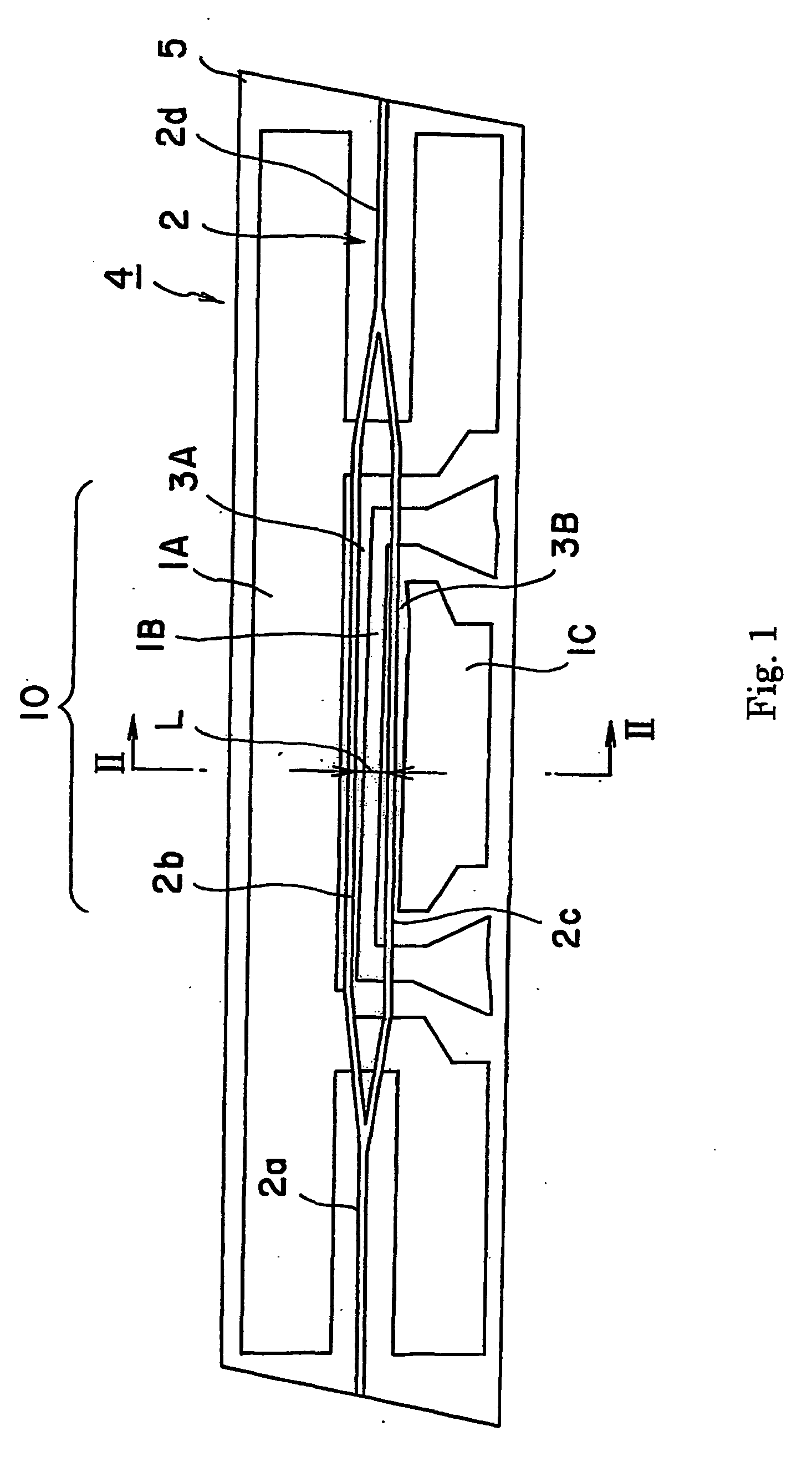
The present invention relates to an optical waveguide device. Prior art which is related to this field of technology can be found e.g. in document An optical modulator, particularly a traveling type optical modulator, using lithium niobate (LiNbO3) lithium tantalate (LiTaO3) or gallium-arsenide (GaAs) for the optical waveguide has excellent properties and may realize a broadband modulation at a high efficiency. Lithium niobate and lithium tantalate are excellent ferroelectric materials having large electro-optic coefficients and can control light within a short optical path. Factors suppressing the modulation speed of the traveling-wave optical modulator include velocity mismatch, dispersion, electrode conductor loss, dielectric loss and mismatch of impedance. Such type of optical modulator normally includes a substrate, an optical waveguide, modulating electrodes including signal and ground electrodes and a buffer layer, and thus has a relatively complex structure. The dimension of each element has been proposed and variously studied until now. The assignee filed a Japanese patent publications Further, so called multi-media industry has been developed and broad band communication has been increasingly demanded, so that it has been already applied an optical communication system operating at a speed higher than 10 Gb/s. Such system operating at even higher speed is expected. An LN optical modulator is applied as a device for modulating electrical signal of 10 Gb/s or higher (microwave signal) to light. It was invented a structure for attaining velocity matching of microwave and light wave to realize wide-band modulation of an optical modulator, by lowering the thickness of an optical waveguide substrate. Further, in the structure having the thinner optical waveguide substrate, it is necessary to reduce the thickness of the substrate around its optical waveguide to about 10 micrometers for satisfying the velocity matching condition. The assignee further filed Japanese patent publication The device described in Japanese patent publication According to the devices of Japanese patent publications According to optical modulators with thin-sheet structure described in Japanese patent publication Nos. An object of the present invention is to improve the extinction ratio characteristic and output power characteristic during on-time in an optical waveguide device comprising a substrate of an electro-optic material, an optical waveguide and a modulation electrode wherein said substrate has a thickness of 30 Further, the assignee has reached the idea of joining a supporting body with an adhesive layer of a substantially uniform thickness on the back face of a thin optical waveguide substrate having a thickness of 30 µm or smaller, as described in Japanese patent publication No. However, a DC drift was observed due to stress generated by the difference of thermal expansion of the optical waveguide substrate and supporting body so as to cause hysteresis in the curve of extinction ratio. When an optical modulator is driven, the bias point is generally shifted at an intermediate point (V/(π/2)) of the maximum and minimum values of optical power by means of an auto bias control circuit. When the hysteresis phenomenon is observed as shown in Further, long-term DC drift is generated to result in a drift of the above bias point so that an auto bias control circuit cannot follow the drift. According to the present invention, it is an option to prevent the hysteresis phenomenon in optical power and long-term DC drift when a signal voltage is applied to an optical waveguide device. The above is accomplished by what is set forth in the appended independent, wherein advantageous modifications are defined in the appended dependent claims. The inventors have studied the cause of the deviation of extinction ratio depending on the wavelength described above in detail and found the followings. That is, when the thickness of the substrate is as small as, for example, 30 Based on the above findings, the present inventors tried to make light propagating in single mode at least around the outlet part of an optical waveguide at least in horizontal direction, when the thickness of the substrate of an electro-optic single crystal is 30 µm or smaller. It is thus found that the deviation of the operational point of the applied voltage and extinction ratio depending on wavelength can be prevented. The "the outlet part" means an optical waveguide elongating straightforwardly after light propagating in Y-shaped branched optical waveguide is optically coupled. Until now, it has not been known that it may occur the deviation of the operational point of the applied voltage and extinction ratio depending on wavelength when the thickness of the optical waveguide substrate is 30 The present invention is realized only after the discovery of the above problems and the cause, and provides great use value in the industry. Further, the inventors have studied the conditions of producing an optical waveguide for making light propagating in single mode in at least horizontal direction of an optical waveguide. It was found that the diffused region forms a swell during the production of an optical waveguide and the shape of the swell and the mode condition of the optical waveguide are correlated with each other. Specifically, the shapes of the optical waveguide and the swells were tested by means of a laser microscope. As a result, it was found that the conditions for single mode propagation of the optical waveguide at least in the horizontal direction is as follows. (A product (H x W) of the height "H" (angstrom) of a swell formed during the formation of an optical waveguide and the width "W" (µ m) of the swell ≤ 7150 angstrom µm) It is thus successfully improved the extinction ratio characteristic. Though, according to the present invention, H x W is set to 6000 angstrom, µm or smaller. When H - W becomes too small, the mode diameter becomes large so that the coupling loss with an outer optical fiber becomes larger. On the viewpoint of reducing the coupling loss, H x W may preferably be 3000 angstrom· µm or larger, and more preferably be 3400 angstrom· µm or larger. According to a preferred embodiment, H ≤ 1100 angstrom and W ≤ 6.5 µm are satisfied. It is thus possible to reduce the dependency of the positions of peak and bottom of the extinction ratio curve on voltage. The inventors have further reached the following discovery. That is, when light is propagated in an optical waveguide in single mode at least in horizontal direction, the mode size is widened so that the mode coupling of the optical waveguides in the waveguide part (interacting part with an electrode) of a Mach-Zehnder interferometer is increased. As a result, the branching ratio may be shifted to deteriorate the extinction ratio. The dependency of the extinction ratio on wavelength becomes large. On the contrary, it is possible to improve the extinction ratio to a value of 20 dB or more by elevating a distance between branched optical waveguides to 46 µm or more. It is thus found that the dependency of the extinction ratio on wavelength can be also reduced. Further according to the present invention an optical waveguide device comprises an optical waveguide substrate, a supporting body for supporting the optical waveguide substrate and an adhesive layer for adhering the optical waveguide substrate and the supporting body. The optical waveguide substrate may comprise a plate-shaped main body comprising an electro-optic material, first and second main faces opposing each other and a thickness of 30 µm or smaller, an optical waveguide provided on the main body and an electrode provided on the main body. The adhesive layer adheres the supporting body and the second main face of the main body. The minimum value of the thermal expansion coefficient of the supporting body may be 1/5 or larger of the minimum value of the thermal expansion coefficient of the main body, and the maximum value of the thermal expansion coefficient of the supporting body may be 5 times or smaller of the maximum value of the thermal expansion coefficient of the main body. When a plate-shaped main body has a thickness of 30 µm or smaller, and a supporting body and main body are adhered with an adhesive layer, it is thus possible to prevent the position of stress concentration in an optical waveguide substrate to disperse the stress and to reduce the maximum stress applied on the optical waveguide substrate. Further, grinding process can be applied for processing the substrate to produce a thin plate, so that processing damage can be considerably prevented by means of an appropriate method and the deterioration of the fracture strength can be prevented at the same time. Simultaneously, when the minimum of the thermal expansion coefficient of the supporting body is made 1/5 or larger of the minimum value of the thermal expansion coefficient of the optical waveguide substrate, and the maximum value of the thermal expansion coefficient of the supporting body is made 5 times or smaller of the thermal expansion coefficient of the optical waveguide substrate, it is thus possible to prevent the hysteresis phenomenon of optical power when a signal voltage is applied and the long-term DC drift can be reduced. The reason for such advantageous effects is not clear. However, " The present invention will be described further in detail referring to the attached drawings. The main body 5 has a shape of a flat plate. Ground electrodes 1A, 1C and a signal electrode 1B are formed on a first main face 5a of a substrate 5. According to the present example, electrode configuration of so called Coplanar waveguide (CPW electrode) is applied. An optical waveguide 2 has an inlet part 2a, an outlet part 2d and a pair of branched parts 2b and 2c. In a region 10 for applying an electric field, a pair of branched parts 2b and 2c of an optical waveguide are positioned between adjacent electrodes, so that a signal voltage can be applied on the optical waveguides 2b and 2c substantially in a horizontal direction. The optical waveguide 2 constitutes an optical waveguide of so-called Mach-Zehnder type. The distance L between the branched parts 2b and 2c is preferably 46 µm or longer. The inventors have further reached the following discovery. The mode coupling of the optical waveguides is problematic in waveguide part of a Mach-Zehnder interferometer (interaction part with an electrode). As to the problem, it is found that the mode coupling between the optical waveguide parts can be reduced by forming a groove 5c between the branched optical waveguide parts as shown in A buffer layer may be provided between the main body and electrodes. Further, the present invention may be applied in the case where the electrode configuration is of asymmetrical coplanar strip line type. The main body is made of a single crystal lithium niobate. The materials of the ground and signal electrodes are not particularly limited as far as the material is excellent in impedance characteristic, and may be composed of gold, silver, copper or the like. The buffer layer may be made of known materials such as silicon oxide, magnesium fluoride, silicon nitride and alumina. The optical waveguide is a titanium diffusion optical waveguide or proton exchange optical waveguide, and most preferably be titanium diffusion optical waveguide. The electrode is formed on the first main face of the main body. The electrode may be directly formed on the first main face or may be formed on the buffer layer. The following ranges are most preferred conditions for producing an optical waveguide.
In the main body, the polarization axis of the crystal is substantially parallel with the first main face 5a of the substrate, which is an X-plate lithium niobate single crystal. It is preferred to further provide a buffer layer between the surface of the substrate and electrode for reducing the propagation loss of light. According to the present invention, as shown in The method of joining the optical waveguide substrate 5 and supporting body 7 is not particularly limited. According to a preferred embodiment, both are adhered. In this case, the refractive index of the adhesive agent may preferably be lower than that of the electro-optic material forming the main body 5. Specific examples of the adhesive agent include an epoxy resin type adhesive, a thermal setting resin type adhesive and an ultraviolet curable resin type adhesive. Such adhesive may preferably have a thermal expansion coefficient relatively close to that of a material having electro-optic effects such as lithium niobate. Preferred embodiments of the second aspect of the invention will be described further in detail referring to drawings. An optical modulator 11 has an optical waveguide substrate 29 and a supporting body 12. Each of the main body 14 and substrate 12 has a shape of a flat plate. The thickness of the main body 14 is 30 m or smaller. Predetermined electrodes 17A, 17B and 17C are formed on a first main face 14a of a main body 14. According to the present example, although so called coplanar type electrode (CPW electrode) configuration is applied, the position and shape of the electrodes are not particularly limited. For example, ACPS type (Asymmetric coplanar strip-line type) may be applied. According to the present example, a pair of optical waveguides 15b and 15c are formed between adjacent electrodes, so that a signal voltage can be applied onto the optical waveguide parts 15b and 15c, respectively, substantially in a horizontal direction. The optical waveguide constitutes so called Mach-Zehnder type optical waveguide in a plan view, and the planar pattern is well known (described later). An adhesive layer 13 having a uniform thickness is interposed between the second main face 14d of the main body 14 and the adhesive face 12a of the supporting body 12, so that the main body 14 and supporting body 12 are joined with each other. According to the optical waveguide device 11, a flat-plate shaped main body having a thickness of 30 µm or smaller is used and adhered with a supporting body with an adhesive, and the adhesion face 12a of the supporting body is made substantially flat. The thickness of the adhesive layer 13 is thus made substantially constant so that the position of stress concentration can be prevented in an optical waveguide device 29. The stress is thus dispersed to reduce the maximum stress in the optical waveguide substrate 29. Further, flat grinding can be used for processing the main body 4 to a thickness of 30 µm or smaller, so that processing damage can be considerably reduced by an appropriate means and the deterioration of the fracture strength can be prevented at the same time. According to the present invention, a main body 14 is composed of a flat plate having a thickness of 30 µm. The flat plate herein described means a flat plate wherein a recess or groove is not formed on the main faces 14d. That is, the second face 14d (adhesion face) is substantially flat. Although the main face 14d is substantially flat, a surface roughness remaining on the surface due to the processing is permitted, and curvature and warping due to the processing are also permitted. According to the present invention, optical waveguides 15b and 15c are provided on the side of the first main face 14a of the main body 14. The optical waveguide may be a ridge type optical waveguide directly formed on the first main face of the main body, or a ridge type optical waveguide formed on another layer on the first main face of the main body, or an optical waveguide formed by inner diffusion or ion exchange process in the inside of the main body, such as titanium diffusion or proton exchange waveguide. Specifically, the optical waveguide may be a ridge type optical waveguide protruding from the main face 14a. The ridge type optical waveguide may be formed by laser or mechanical processing. Alternatively, a film of a high refractive index may be formed on the main body 14 and then processed by mechanical or laser ablation processing to produce a ridge type three-dimensional optical waveguide. The film of a high refractive index may be formed, for example, by chemical vapor deposition, physical vapor deposition, organic metal chemical vapor deposition, sputtering or liquid phase epitaxy process. The main body forming the optical waveguide substrate is composed of a single crystal. In the main body, the polarization axis of the crystal is substantially parallel with the first main face (surface) of the substrate, which is an X-plate lithium niobate single crystal. It is preferred to further provide a buffer layer between the surface of the substrate and electrode for reducing the propagation loss of light. According to the present invention, the minimum value of the thermal expansion coefficient of the supporting body may be 1/5 or larger of the minimum value of the thermal expansion coefficient of the main body, and the maximum value of the thermal expansion coefficient of the supporting body may be 5 times or smaller of the maximum value of the thermal expansion coefficient of the optical waveguide substrate. When each of the electro-optic materials forming the main and supporting bodies has no anisotropy in thermal expansion coefficient, the minimum and maximum values of the thermal expansion coefficient are the same in each of the main and supporting bodies. When each of the electro-optic materials forming the main and supporting bodies is anisotropic in thermal expansion coefficient, the thermal expansion coefficient may be changed for the respective axes. For example, when the electro-optic material forming the main body is lithium niobate, the thermal expansion coefficients for X axis and Y axis are 16 x 10-6 /°C, respectively, which is the maximum value. The thermal expansion coefficient in Z axis is 5 x 10⁻⁶ /°C, which is the minimum value. Therefore, the minimum value of the thermal expansion coefficient of the supporting body is made 1 x 10⁻⁶ /°C or larger, and the maximum value of the thermal expansion coefficient of the supporting body is made 80 × 10-6 /°C or smaller. For example, the thermal expansion coefficient of quartz glass is 0.5 × 10⁻⁶/°C and thus smaller than 1 × 10⁻⁶ /°C, for example. On the viewpoint of the advantageous effects of the present invention, the minimum value of thermal expansion coefficient of the supporting body may more preferably be 1/2 or larger of that of the main body. Further, the maximum value of thermal expansion coefficient of the supporting body may more preferably be 2 times or smaller of the maximum value of that of the main body of the optical waveguide substrate. Specific examples of the material of the supporting body is not particularly limited, as far as the above conditions are satisfied. When lithium niobate single crystal is used for the main body, the material of the supporting body includes lithium niobate, lithium tantalate, a solid solution of lithium niobate-lithium tantalate and potassium lithium niobate. In this case, lithium niobate same as the material of the main body is most preferred on the viewpoint of a difference of thermal expansion. The electrodes are provided on the first main face of the main body. The electrodes may be provided directly on the first main face of the main body, or provided on a low dielectric constant layer or a buffer layer. The low dielectric layer may be made of a known material such as silicon oxide, magnesium fluoride, silicon nitride or alumina. The term "low dielectric layer" means a layer composed of a material having a dielectric constant lower than that of the material forming the main body. The dielectric constant of the material may be preferably lower on the viewpoint of satisfying the velocity matching condition of light and micro wave. When the low dielectric layer is not present, the thickness of the main body may preferably be 20 µm or smaller. According to a preferred embodiment, the face 12a for adhesion of the supporting body 12 is substantially flat. The phrase "the face 12a for adhesion is substantially flat" means that surface roughness remaining after the processing and curvature and warping due to the processing are allowed. On the viewpoint of the present invention, the thickness T1 of the adhesive layer 13 may preferably be 1000 Further, on the viewpoint of velocity matching, it is required that the dielectric constant of the adhesive layer is lower than that of the electro-optic material forming the main body, and the dielectric constant may preferably be 5 or lower. An optical modulator 11A has an optical waveguide device 29 and a supporting body 32. The main body 14 has a shape of a flat plate, and the thickness of the main body 14 is 30 According to the present example, an adhesive layer 33 is interposed between the second main face 14d of the main body 14 and the face 32a for adhesion of the supporting body 32 to adhere the main body 14 and supporting body 32. At the same time, a groove 32b is formed under the main face 14d in regions where optical waveguides 15b and 15c are formed. An adhesive is filled in the groove 32b to form a low dielectric portion 36. According to the optical waveguide device 11A, the flat-plate shaped main body 14 having a thickness of 30 According to the present embodiment, however, the thickness T2 of the low dielectric portion 36 made of an adhesive agent is made larger than that of the thickness T1 of the adhesive layer 33, so that a step having a height of (T2-T1) is formed in the thickness of the adhesive layer. Different from the device whose adhesive layer has a constant thickness over the whole length, the concentration of stress may be easily caused in the main body 14 around the step. The thickness T1 of the adhesive layer 33 may preferably be 200 µ m or smaller, for reducing the DC and temperature drifts due to such concentration of stress. On the viewpoint, it is required that the thickness T1 of the adhesive layer 33 is 200 According to the present invention, the adhesive layer may adhere the second main face and supporting body in a region where an optical waveguide is formed. For example, the optical waveguide devices 11 of Further, according to the present invention, it is preferred to provide a low dielectric portion having a dielectric constant lower than that of the electro-optic material forming the main body between the second main face and supporting body in a region where optical waveguide is formed. It is thus possible to facilitate the velocity matching as described above. The kind of the low dielectric portion is not particularly limited. According to a preferred embodiment, the low dielectric portion is an air layer. Further in another preferred embodiment, the low dielectric part is composed of an adhesive (examples of Further, according to another embodiment of the present invention, the low dielectric portion is composed of a low dielectric material having a dielectric constant lower than that of the electro-optic material, and the low dielectric material does not belong to an adhesive. According to the present example, adhesive layers 43A and 43B are provided between the second main face 14d of the main body 14 and the adhesion face 32a of the supporting body 32 to adhere the main body 14 and supporting body 32. The groove 32b is formed to provide a low dielectric portion 30 under the main face 14d in regions where optical waveguides 15b and 15c are formed. The low dielectric portion 30 according to the present example is composed of a low dielectric material different from adhesives 43A and 43B. According to the present example, adhesive layers 44A and 43B are provided between the second main face 14d of the main body 14 and the adhesion face 12a of the supporting body 12 to adhere the main body 14 and supporting body 12. An air layer 31 is formed under the main face 14d in regions where optical waveguides 15b and 15c are formed. The air layer 31 functions as a low dielectric portion. According to the present example, adhesive layers 43A and 43B are provided between the second main face 14d of the main body 14 and the adhesion face 32a of the supporting body 32 to adhere the main body 14 and supporting body 32. The thickness T1 of each of the adhesive layers 43A and 43B is 200 On the viewpoint of velocity matching, the thickness T2 of the low dielectric portion 30, 35 or 36 may preferably by 10 The present invention may be also applied to a traveling wave type optical modulator of so-called independent modulation type. The material of the electrode is not particularly limited, as far as it has superior impedance property and a low resistance. The material may be gold, silver copper or the like. Specific examples of the adhesives are not particularly limited as far as the above conditions are satisfied, they include an epoxy resin type adhesive, thermal setting resin type adhesive, ultraviolet curable resin type adhesive and "Alon Ceramics C" (trade name: manufactured by Toa Gosei: thermal expansion coefficient of 13 × 10-6 K) having a thermal expansion coefficient relatively close to that of the material having electro-optic effect such as lithium niobate. Further, the adhesive glass may preferably be that having a low dielectric constant and a temperature suitable for adhesion (working temperature) of about 600 °C or lower. Further, it is preferred that a sufficient adhesive strength can be obtained after the processing. Specifically, so-called solder glass containing a composition of a plurality of ingredients such as silicon oxide, lead oxide, aluminum oxide, magnesium oxide, calcium oxide, boron oxide or the like. Further, a sheet of an adhesive may be provided between the back face of the main body 14 and the supporting body to adhere them. Preferably, a sheet made of a thermal setting, light curable or light thickening resin adhesive is provided between the back face of the main body 4 and the supporting body and cured. A Ti diffusion waveguide and CPW electrode pattern were formed on a lithium niobate substrate of X-cut (see Further, the height "H" and width "W" of the swell of an optical waveguide were changed as shown in According to the comparison of tables 1 and 2, multi mode propagation was observed in a wide range as shown in table 1, even under the condition of dimensions of single mode when the thickness of the substrate of electro-optic crystal was large (table 2). Further, when the thickness of the substrate is 1 mm, the optical waveguide was made cut-off to prevent the propagation of light therein when the width of the optical waveguide is 6 It was proved to be necessary to adjust H × W at a value of 7150 angstrom · In the Example 1, the distance "L" between optical waveguide arms was 55 S21 of the device was measured to prove that no ripple was found in a wavelength range of 50 GHz or lower, the curve of the graph was smooth and was lowered by minus 6 dB only in a range of 30 GHz or higher. Further, S11 was minus 10 dB or larger in a measured range of up to 50 GHz. Further, the mode was observed as an optical property. The observed mode proved to be single mode, the extinction ratio was 20 dB or more in a range of 1530 nm to 1610 nm, and the dependency of extinction ratio curve on voltage was proved to be small and ± 5 percent or smaller. Further, the dependency of extinction ratio on wavelength was shown in In the Example 1, the gap between the central electrode 1B and ground electrode 1A or 1C was made 40 S21 of the device was measured to prove that no ripple was found in a wavelength range of 50 GHz or lower, the curve of the graph was smooth and was lowered by minus 6 dB only in a range of 25 GHz or higher. Further, S11 was minus 10 dB or smaller in a measured range of up to 50 GHz. Further, the mode was observed as an optical property. The observed mode proved to be single mode, the extinction ratio was 20 dB or more in a range of 1530 nm to 1610 nm, and the dependency of extinction ratio curve on voltage was proved to be small and ± 5 percent or smaller. A thin type modulator was produced according to the same procedure as the Example 2. The distance between optical waveguide arms was 55 A thin type modulator was produced according to the same procedure as the Example 2. The width of the central electrode was made 20 µm and the distance between optical waveguide arms was made as small as 45 A thin type modulator was produced according to the same procedure as the Example 2. The width of the central electrode was made 20 A thin type modulator was produced according to the same procedure as the Example 2. The distance between optical waveguide arms was 55 Further, the mode was observed as an optical property. The observed mode proved to be multi mode. The extinction ratio was lower than 20 dB in a part of a range of 1530 nm to 1610 nm, and the dependency of extinction ratio curve on voltage was proved to be larger than ± 5 percent. Further, the dependency of extinction ratio on wavelength was shown in A device was produced according to the same procedure as the Example 2. The height of the recess was 860 angstrom, the width was 5 A device was produced according to the same procedure as the Example 2. The height of the recess was 1150 angstrom, the width was 5 An optical modulator 11 of According to the present example, the substrate of X-cut 3 inch wafer (LiNbO3 single crystal) was used. The thermal expansion coefficients in the X-axis and Y-axis are 16 × 10-6/°C, respectively, and the thermal expansion coefficients in the Z-axis is 5 × 10⁻⁶/°C. The material of the supporting body 2 was x-cut lithium niobate single crystal. The extinction curve with respect to a signal of 1KHz is shown in The device 11C of Hysteresis was not observed in the extinction curve with respect to a signal of 1KHz. Further, the DC drift was evaluated at 100 °C to prove that the shift amount of the DC bias was within a deviation of 50 percent with respect to the initial applied voltage. The device 11A of Hysterisis was not observed in the extinction curve with respect to a signal of 1KHz. Further, the DC drift was evaluated at 100 °C to prove that the shift amount of the DC bias was within a deviation of 50 percent with respect to the initial applied voltage. The device 11D of Hysteresis was not observed in the extinction curve with respect to a signal of 1KHz. Further, the DC drift was evaluated at 100 °C to prove that the shift amount of the DC bias was within a deviation of 50 percent with respect to the initial applied voltage. In the same structure as that shown in No hysteresis was found in the extinction curve with respect to a signal of 1kHz. Further, the DC drift was evaluated at 100 °C to prove that the shift amount of the DC bias was within a deviation of 50 percent with respect to the initial applied voltage. According to the present example, a substrate made of 3 inch wafer of x-cut (LiNbO3 single crystal) was used. The thermal expansion coefficients in the X-axis and Y-axis are 16 × 10 -6/°C, respectively, and the thermal expansion coefficient in the Z-axis is 5 × 10 6/°C. The material of the supporting body 2 was quartz glass whose thermal expansion coefficient is 50 × 10-6/°C. No hysteresis was found in the extinction curve with respect to a signal of 1 kHz. Further, the DC drift was evaluated at 100 °C to prove that the shift amount of the DC bias was out of a deviation of 50 percent with respect to the initial applied voltage. According to the invention, it is possible to prevent hysteresis phenomenon in optical power upon the application of a signal voltage and long-term DC drift in an optical waveguide device. An optical waveguide device comprising
a substrate (5) of X-cut lithium niobate single crystal; signal (1B) and ground electrodes (1A, 1C) for modulation formed on a first main face (5a) of the substrate (5); and a titanium diffusion optical waveguide (2) provided between said signal (1B) and ground electrodes (1A, 1C) and comprising an inlet part (2a), an outlet part (2d), and a pair of branched parts (2b, 2c), wherein in a region for applying an electric field, the pair of branched parts (2b, 2c) is positioned between adjacent electrodes so that a signal voltage can be applied on the branched parts (2b, 2c); wherein said substrate (5) has a thickness of 30 µm or smaller at least in the region where signal (1B) and ground electrodes (1A, 1C) can apply an electric field, and wherein the optical waveguide device further comprises a supporting body (7) for supporting said substrate (5) and an adhesive layer for adhering said substrate (5) and said supporting body (7); The optical waveguide substrate of claim 1, wherein said branched parts (2b, 2c) are distant from each other by 46 µm or larger. The optical waveguide device of claim 1, wherein a groove (5c) is formed in said substrate (5) between said branched parts (2b, 2c). The optical waveguide device of any one of claims 1 to 3, wherein the minimum value of a linear thermal expansion coefficient of said supporting body (7) is 1/5 or larger of the minimum value of a linear thermal expansion coefficient of said substrate (5), and wherein the maximum value of a linear thermal expansion coefficient of said supporting body (7) is 5 times or smaller of the maximum value of a linear thermal expansion coefficient of said substrate (5). The optical waveguide device of claim 4, wherein said supporting body (7) comprises one or more material(s) selected from the group consisting of lithium niobate, lithium tantalate, a solid solution of lithium niobate-lithium tantalate and potassium lithium niobate. The optical waveguide device of any one of claims 1 to 5, wherein said supporting body (7) comprises lithium niobate single crystal. The optical waveguide device of any one of claims 1 to 6, wherein said swell has a height H of 1100 angstrom or lower and a width "W" of 6.5 µm or smaller.BEST MODES FOR CARRYING OUT THE INVENTION
EXAMPLES
(Example 1)
3 2.2 1.8 1.4 1.4 Single Single Single Single 2250 2550 3300 3450 4 1.85 1.3 1.22 1.3 Single Single Single Single 3000 3400 4400 4600 5 1.65 1.1 1.09 1 Single Single Single Single 3750 4250 5500 5750 6 1.5 1.05 1 0.9 Single Single Single Single 4500 5100 6600 6900 6.5 1.45 1.02 0.98 0.9 Single Single single Multi 4875 5525 7150 7475 7 1.35 1 0.95 0.9 Single Single Multi Multi 5250 5950 7700 8050 8 1.3 0.95 0.95 0.85 Single Single Multi Multi 6000 6800 8800 9200 9 1.2 0.95 0.9 0.85 single Multi Multi Multi 6750 7650 9900 10350 Notes: upper column: Mode size of an optical waveguide in horizontal direction, provided that 1 is assigned to the mode size of a 1.55 µm band Panda fiber in horizontal direction (direction of slow axis) 3 1150 1.4 Single 3 4 5 0 4 1150 1.2 Single 4 6 0 0 5 1150 1 Single 5 7 5 0 6 1150 0.9 Single 6 9 0 0 7 1150 0.85 Single 8 0 5 0 9 1150 0.85 Multi 1 0 3 5 0 1: Mode size of an optical waveguide in horizontal direction, provided that 1 is assigned to the mode size of a 1.55 µ m band Panda fiber in horizontal direction (direction of slow axis) (Example 2)
(Example 3)
(Example 4)
(Example 5)
(Example 6)
(Comparative Example 1)
(Example 7)
(Example 8)
(Example 9: Device 11 of Fig. 6)
(Example 10: Device 11C of Fig. 9)
(Example 11: Device 11A of Fig. 7)
(Example 12: Device 11D of Fig. 10)
(Example 13: Device 11 of Fig. 6)
(Comparative example 2: Device 11 of Fig. 6)
the optical waveguide (2) is configured for single mode propagation in the 1.55 µm band, and each
of the branched parts (2b, 2c) of said optical waveguide (2) comprises a swell (6) with respect to the main face (5a) of said substrate (5), said swell (6) when viewed in a cross section taken perpendicularly to the extension direction of the branched parts (2b, 2c) having a height H (Ångstrom) defined as a peak height value and a width W (µm) defined as a distance between two most distant points selected from all the points whose heights are 5 percent of the height H whose product (HxW) is 6000 Ångstrom·µm
or smaller and 3000 Ångstrom·µm or larger.