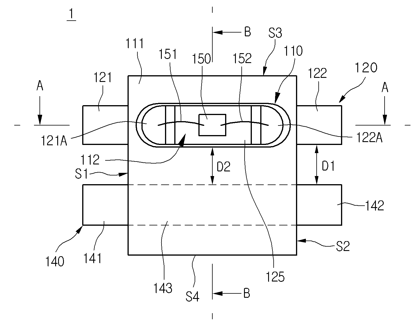
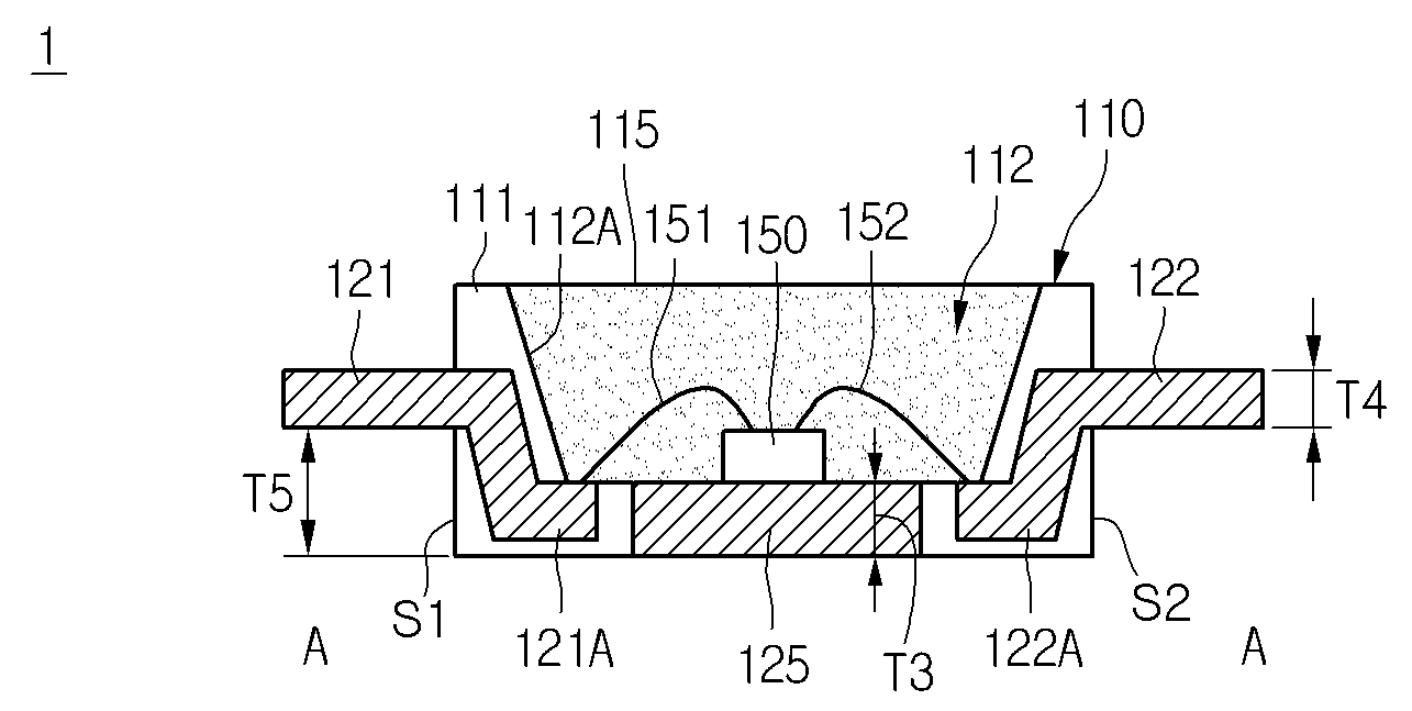
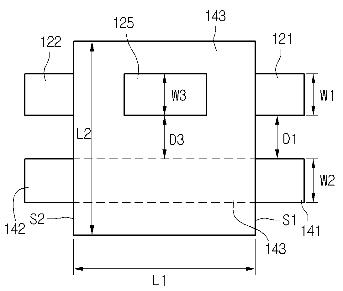
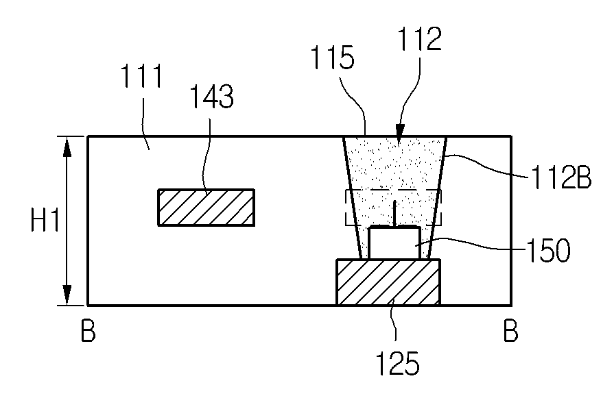
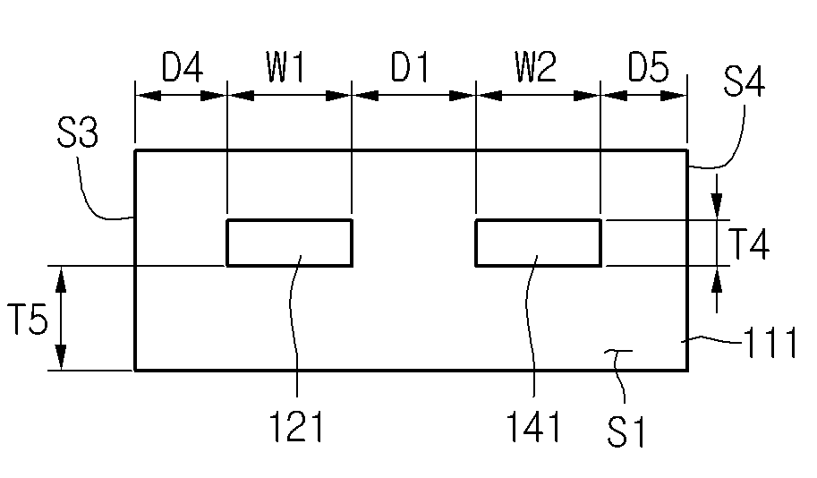
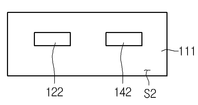
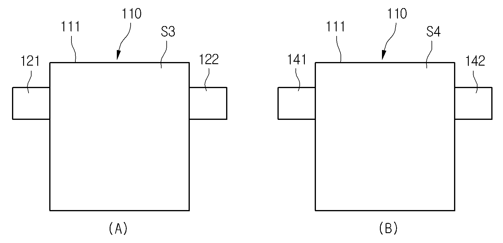
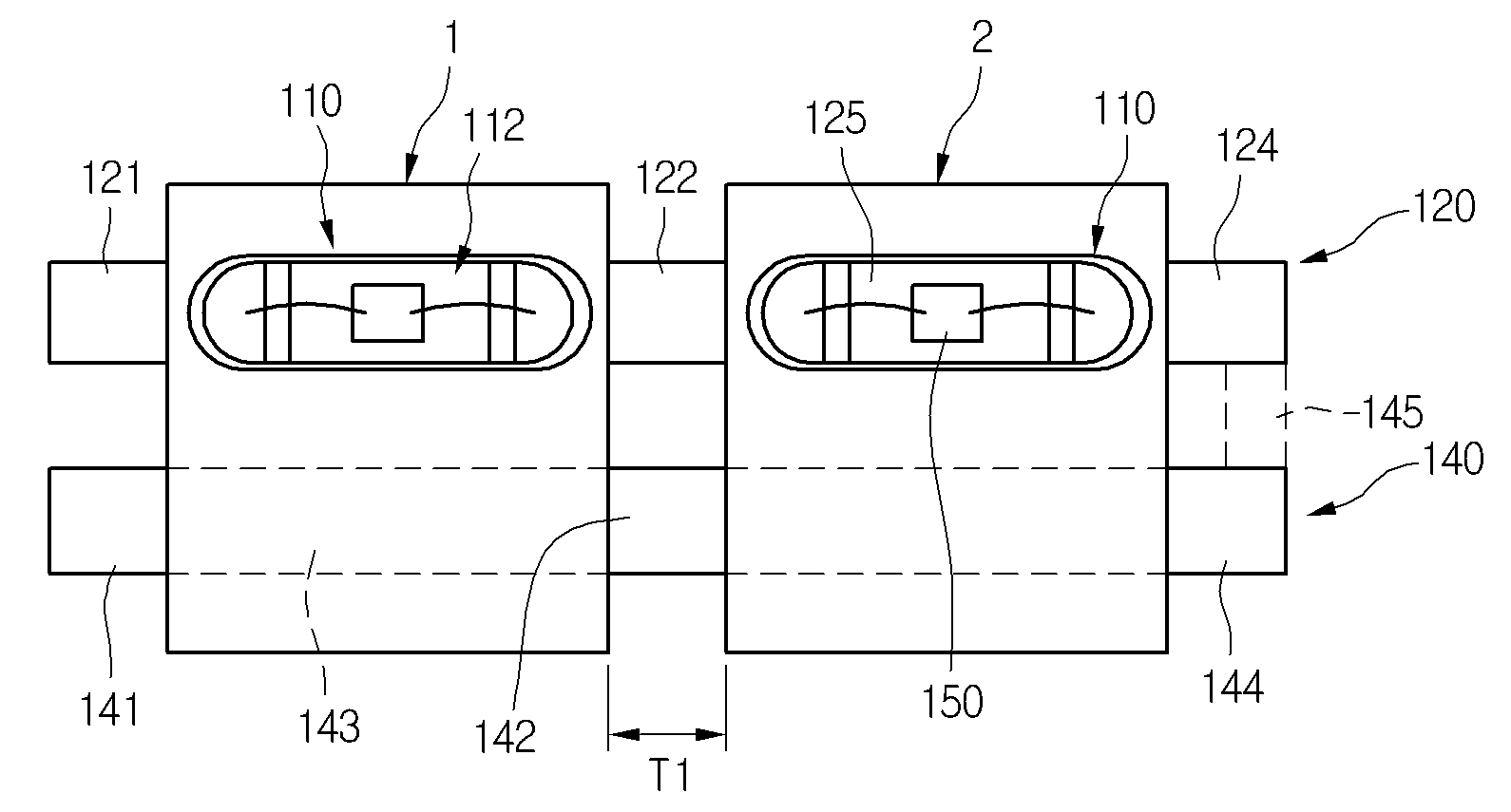
라이트 유닛 및 이를 구비한 발광 장치
The light emitting device having the same light guide embodiment examples are disclosed. Light emitting diode (LED) light electrical energy conversion semiconductor electromagnetic wave is disclosed. The light emitting diode fluorescent lamp, incandescent lamp such as compared to existing low power light source, a semi-permanent life, fast response time, safety, environment friendly benefits have. The progressing forward more for replacing existing light source and light-emitting diodes, the light emitting diode used in indoor or outdoor knob, liquid crystal display device, electric, light sources such as street lighting device used as well as increased and are disclosed. An example embodiment of the light emitting chip inside the body and at least 2 light-emitting element including plurality of frames that are arranged in rows number [...] substrate. An example embodiment of light emitting elements having the same light emitting device arranged to support a light guide frame between a number [...] substrate. Example embodiment a plurality of light emitting elements disposed through the conductive frame number 1 number 2 connected to the conductive frame including said number 1 conductive frame one end-UV light unit and a device number [...] substrate. An example embodiment of light emitting elements having roof frame through a light emitting device attached with the aid of adhesive member writing unit number [...] substrate. Light unit according to the example embodiment, number 1 body having a cavity therein, said number 1 number 1 including blue light of light emitting elements disposed in the cavity; said number 1 cavity and electrically connected to said number 1 in regular intervals, said plurality of light emitting elements between connecting the plurality of frame parts including connecting frame; and said number 1 spaced from the cavity, penetrate the inside of the body by said plurality of said plurality of light emitting elements comprises a connection between the roof frame. Light unit according to the example embodiment, a blue light emitting device having a plurality of number 1; said number 1 light-emitting device having light-emitting chip connected with at least 2 of frame number 1 connecting frame; said plurality of number 1 disposed spaced apart from said number 1 connecting frame number 1 loop frame including number 1 LED light unit; and A blue light emitting device having a plurality of number 2; said number 2 light-emitting device having light-emitting chip connected with at least 2 of frame number 2 connecting frame; said plurality of number 2 LED light unit including number 2 which passed through said number 2 number 2 loop frame spaced apart from the connecting frame, the other end of the roof frame said number 1 number 1 connecting frame is composed of said number 1 light unit, said number 1 and number 2 number 1 corner of the roof frame said number 2 that are connected together with one end of the connecting frame corner of the light emitting device. The light emitting device according to embodiment example, number 1 body having a cavity therein, said number 1 number 1 disposed within a chip including a plurality of light emitting elements; said number 1 cavity and electrically connected to said number 1 in regular intervals, said plurality of light emitting elements between connecting the plurality of frame parts including connecting frame; and said number 1 spaced from the cavity, said light emitting diodes of said plurality of light emitting elements through the body making a connection between the loop frame including light unit; metal plate below said light unit light-emitting elements; and a plurality of light-emitting element comprising said metal plate between said adhesive member. To simplify the process for preparing example embodiment can be package number. Example embodiment individual light-emitting device can be supplied from a mounting process (SMT process). An example embodiment is wherein the loop, loop pattern without using a board that has a thereof can. An example embodiment for arranging individual light emitting element can be mounted using the photoresist pattern series, number tank can be installed. An example embodiment of light unit having the same light emitting device and improve radiation efficiency is not disclosed. Example embodiment between board pattern self frame using a light-emitting element not by soft deficiency, having the same light emitting device improving the reliability of a light guide is not disclosed. Figure 1 shows a plane of the light unit according to example number 1 embodiment also are disclosed. Figure 2 shows a plane view of Figure 1 indicating one example of a light emitting device are disclosed. Figure 3 shows a A provided A side cross-sectional drawing of Figure 2 are disclosed. Figure 4 shows a rear view of a light emitting device of Figure 2 also are disclosed. Figure 5 shows a light-emitting device B provided B side cross-sectional drawing of Figure 2 are disclosed. Number 1 side view of Figure 2 Figure 6 shows a light-emitting device are disclosed. Number 2 side view of Figure 2 Figure 7 shows a light-emitting device are disclosed. (A) (B) number 3 side view and number 4 side view of Figure 2 of Figure 8 includes a light-emitting device are disclosed. Figure 9 shows a plane of the light unit according to example number 2 embodiment also are disclosed. The sides of the cross-sectional drawing of Figure 9 Figure 10 shows a light unit are disclosed. Figure 11 shows a corner of the rear view of Figure 9 also are disclosed. Drawing number 14 to number 3 embodiment according to example 12 also includes indicating light unit are disclosed. Figure 15 shows a number 4 embodiment example according to the indicating light unit also are disclosed. Figure 17 shows a coupling between the light unit according to example 16 and also indicating the example number 5 embodiment also are disclosed. Figure 18 shows a light emitting device according to example indicating the number 6 embodiment also are disclosed. Figure 19 shows a cross-section indicating a display device also number 7 embodiment example according to of Figure 1 light unit are disclosed. Figure 20 shows a cross-section indicating a display device according to of Figure 1 light unit number 8 embodiment example also are disclosed. Figure 21 shows a lighting device according to of Figure 1 light unit indicating the example number 9 embodiment also are disclosed. Figure 23 shows a light unit and light-emitting elements according to example 22 and also indicating the number 10 embodiment also are disclosed. Figure 25 shows a light unit and light-emitting elements according to example 24 and also indicating the number 11 embodiment also are disclosed. Figure 27 shows a light unit and light-emitting elements according to example 26 and also indicating the number 12 embodiment also are disclosed. Figure 28 shows a number 13 embodiment also indicating light unit according to the example are disclosed. Figure 29 shows a light unit indicating the connection between member of Figure 28 also are disclosed. Figure 30 shows a number 14 embodiment also indicating light unit according to the example are disclosed. Figure 39 shows a light unit according to the example embodiment also 31 to light emitting diodes of indicating variants also are disclosed. Figure 46 shows a example according to embodiment also 40 to also emitting, indicating variants of the heat are disclosed. Figure 47 shows a light unit mounted light emitting chip surface-emitting elements according to embodiment example also are disclosed. Figure 48 shows a light unit light-emitting elements according to embodiment example also indicating the way light-emitting chip are disclosed. In the embodiment of in description, each layer (film), region, pattern or structures substrate, each layer (film), region, pad or patterns "on (on)" or "(under) below" when described to be formed in, "on (on)" on "below (under)" is "direct (directly)" or "(indirectly) via another layer" includes both the formation. In addition to drawing of each layer above or below reference reference may be described as follows. Drawing descriptive convenience and clarity or exaggerated in thickness of intermediate magnitude for exposed to determine is also shown. In addition each thread size of the components that reflect the size number entirely are not correct. Figure 1 shows a plane indicating light unit according to example number 1 embodiment also are disclosed. Figure 2 shows a plane view indicating one example of a light emitting device which, also of Figure 2 A provided A cross-sectional drawing and Figure 3 shows a side, rear view of a light emitting device and degrees Figure 4 of Figure 2, and Figure 5 of Figure 2 B provided B cross-sectional drawing side of a light emitting device, light-emitting device number 1 side view and Figure 6 of Figure 2, and Figure 7 of Figure 2 number 2 side view of a light emitting device, number 4 and number 3 side view of Figure 2 (A) (B) side of Figure 1 of Figure 8 includes a light-emitting device are disclosed. The reference also 1, light unit (100) includes a plurality of light-emitting device (11:1) wherein, said plurality of light emitting elements (11) is that are joined together are prevented. Said plurality of light emitting elements (11) is n (n>1) two preset interval (T1) and sequentially connected, said diodes for emitting (1 a-n) includes at least one light emitting unit (110) having a predetermined wavelength. Said light emitting unit (110) includes diodes for emitting said (1 a-n) further includes a groove arranged on one side of center, number 1 (X) direction along heat (row) or the first and second adders are prevented. Wherein, said n is integer more than 2, each light emitting chip (for example: 110V or 220V) divided by the total drive voltage driving voltage or can contain several hundreds - number. Said plurality of light emitting elements (11) is at least 2 or more times higher than the total drive voltage or individual light emitting chip forward of which operates by a smoothing choke coil has to be coated. Said light-emitting device (1 a-n) (T1) spacing between composed a dimension, a random interval, or irregular spacing can be spaced disclosed. Said interval T1 is 0. Can be 1 mm or more of ranges, defined with respect to the not more. Said plurality of light emitting elements (11) and its (110) (T2) is of constant period or irregular period between an inlet can be arranged, defined with respect to the not more. Wherein, two light-emitting elements n (1 a-n) first one of the light-emitting element number 1 light-emitting device (1) and, second light-emitting element number 2 light emitting element (2) and, second light-emitting element emitting n number n (n) can be defined. Said number 1 light-emitting device (1) and one end of the fire number 1 polarity power supply can be powered, the other end of said number n light-emitting device (n) power polarity power supply can be is the number 2. Two light-emitting elements said n (1 a-n) is a plurality of conductive frame is arranged, one conductive frame is said plurality of light emitting elements (11) electrically connects connecting frame (120) and, roof frame for other one conductive frame is loop circuit (140) can be disclosed. Said connecting frame (120) divided into a plurality of frame part (121,122,124) which, conductive frame number 1, number 1 lead frame, or number 1 connecting frame can be defined. Said roof frame (140) comprises at least one contains a frame, return frame, feedback frame, conductive frame number 2, number 2 number 2 lead frame or the column to the connecting frame may be filled. Said connecting frame (120) and said roof frame (140) is said plurality of light emitting elements (11) is arranged number 1 (X) direction is formed. Said connecting frame (120) column on said roof frame (140) when the heat from a top, next to each other or can be disposed parallel to each other. Said light unit (100) testing said number 1 (P1, P2) in the light-emitting device (1) can be connected. (N) said number n light emitting device the connecting member (145) are connected to, said connecting member (145) is said number n light-emitting device (n) coupled with each other. Said connecting frame (120) and said roof frame (140) is made out of a metal material which, for example said metal material, such as conductive material be a lead frame. Said metal material is Cu, Au, Al, Ag, Ni alloy and of selected in at least 2, at least one layer can be formed, defined with respect to the not more. With reference also to the 3 1 also, said connecting frame (120) is said number 1 light-emitting device (1) and projecting number 1 number 1 (S1) of side frame part (121), said diodes for emitting (1 a-n) in the interior of the adjacent light emitting elements (1 a-n) interface between electronic beam emitting elements (1 a-n) interconnecting a plurality of number 2 to frame part (122), and (n) said number n of number 2 (S2) and projecting number 1 end frame portion side light emitting element (124) having a predetermined wavelength. Said number 1 frame portion (121) is said number 1 light-emitting device (1) of light emitting chip (150) connected with the, said number 2 frame portion (122) includes diodes for emitting said (1 a-n) light-emitting chips (150) connected to adjacent light-emitting chip (150) to a Serial connecting to other. Said number 2 frame portion (122) of adjacent light-emitting element 2 is electrically connected to substrate. Said number 1 end frame portion (124) of said number n is number 2 (S2) 2b projects from side light emitting element (n). Said number 1 frame portion (121), number 2 frame portion (122) and number 1 end frame portion (124) is physically separated therefrom. Said roof frame (140) is said number 1 light-emitting device (1) of number 1 (S1) side project number 3 frame portion (141), said luminescence devices (1 a-n) number 4 disposed between the frame part (142), said diodes for emitting (1 a-n) are located inside the number 5 of frame part (143), number 2 (S2) and (n) said number n of light emitting element side and projecting number 2 end frame portion (144) having a predetermined wavelength. Said number 3 frame portion (141), number 4 frame portion (142), number 5 frame portion (143) and number 2 end frame portion (144) is physically connected to the one into the frames of the combustion chamber. Said number 1 frame portion (121) is said light unit (100) and the input of, said number 3 frame portion (141) includes said light unit (100) can be the output of. Said power supply (P1, P2) are used to said input stage and the output stage. Said number 2 frame portion (122) said number 4 on frame part (142) is said light emitting elements (1 a-n) is equal to interval-. Said connecting frame (120) number 1 of end frame portion (124) said number n (n) of light emitting chip includes a light emitting element (150) connected with the, said roof frame (140) number 2 of end frame portion (144) on said connecting frame (120) number 1 of end frame portion (124) is said connecting member (145) can be connected by. Said connecting member (145) is said connecting frame (120) and said roof frame (140) can be formed between the material of the same material. Said connecting member (145) is said roof frame (140) number 2 of end frame portion (144) on said connecting frame (120) number 1 of end frame portion (124) can be integrally formed. As another example, said connecting frame (120) number 1 of end frame portion (124) on said roof frame (140) number 2 of end frame portion (144) are each open to spaced, wire or conductive tape can be connected. Wherein, said wire or conductive tape can be used as a connection member. Said roof frame (140) said number n (n) of the light emitting end frame number 2 (144) on said number 1 light-emitting device (1) of frame part number 3 (141) electrically connected gear, loop circuit formed on the substrate. Said connecting frame (120) number 1 of frame part (121) that are input to the power supply is said number 1 light-emitting device (1) supplied to the light emitting element from said number n (n), (n) said number n light emitting element supplied to said power supply includes roof frame (140) through said number 1 light-emitting device (1) connected to the frame part number 3 (141) is outputted to. Said plurality of light emitting elements (11) includes a board (example: PCB) electrically connected without solder insulating layer, said via power supply (P1, P2) can be driven by a power source. In addition said plurality of light emitting elements (11) is said light unit (100) through thereof can power is supplied to both ends of the channels. The 1, 2 and 4 may also reference, said number 1 frame portion (121) said number 3 on frame part (141) said number 2 (D1) distance between the frame part (122) said number 4 on frame part (142) can be equal to the distance between (D1). the interval D1 0. 5 Mm or more can be spaced disclosed. Said interval D1 part of a supply voltage from said number 1 frame portion (121) said number 3 on frame part (141) or said number 2 frame portion (122) said number 4 on frame part (142) be a distance to set up the interference does not occur. Also such as 2, said light emitting unit (110) said number 5 on frame part (143) D1 (D2) is equal to or other spacing between said interval can be, for example D1 D2 is larger than or equal to said interval said interval thereof can. Figure 5 shows a plurality of light emitting devices to the light-emitting device 2 also indicating one example which also number 1, other light emitting devices include a light-emitting element reference number 1 to less than 1000. The reference also 2 to 5 also, light-emitting device (1) a body (111), said body (111) is opened in the upper surface of cavity (112), said body (111) of the side frame part number 1 number 1 (S1) in a plane (121) and number 3 frame portion (141), said body (111) of the side frame part number 2 number 2 (S2) in a plane (122) and frame part number 4 (142), said cavity (111) and a bottom surface disposed within frame (125), and said heat dissipation frame (125) disposed above said light emitting chip (150) comprises. Said body (111) is chosen amongst the phthalamide (PPA: Polyphthalamide) material such as resin, silicon (Si), metal material, PSG (photo sensitive glass), sapphire (Al2 O3 ), Of at least one of printed circuit board (PCB) can be. Said body (111) (S1, S2, S3, S4) of at least 4 side features with which, for example such as inhaler 6 comprising polyhedron can be, defined with respect to the not more. Said cavity (112) is said body (111) the upper surface of the region number 1 is opened, said body (111) above when open number 1 region is watching, circular, polygonal, such as elliptical can be like, defined with respect to the not more. Said cavity (112) and the shape of the cup-shaped or container shape, defined with respect to the not more. Said light emitting unit (110) is said cavity (112) region of the disclosed. Also such as 3 and 5 also, said cavity (112) side of number 1 (112A) can be obliquely to the bottom of the cavity, said cavity to its tilting angle (112) can be depending on depth of. Said cavity (112) side of number 1 (112A) is realized can be structure, defined with respect to the not more. Said cavity (112) side of number 1 (112A) and number 2 adjacent side (112B) is made for conveniently discharging area between the angle can be formed. Wherein, said cavity (112) of number 1 and number 2 side (112A, 112B) can be obliquely different angle, defined with respect to the not more. Said cavity (112) in said number 1 frame portion (121) of bonding part number 1 (121A), heat dissipation frame (125), number 2 frame portion (122) of bonding part number 2 (122A) is disposed thereon. Said heat dissipation frame (125) is said number 1 frame portion (121) of bonding part number 1 (121A) said number 2 on frame part (122) of bonding part number 2 (122A) can be disposed between. Said number 1 frame portion (121) of bonding part number 1 (121A), heat dissipation frame (125), and said number 2 frame portion (122) of bonding part number 2 (122A) or electrical efficiency of the position of the package can be modified for the reliability. Said number 1 frame portion (121) is said body (111) side of number 1 (S1) in said body (111) through an interior of said cavity (112) extending to the bottom of the, said number 2 frame portion (122) includes said body (111) side of number 2 (S2) in said body (111) through an interior of said cavity (112) extending to the bottom of. Said heat dissipation frame (125) 3 is photosensitive resin composition such as body (111) can be exposed on the lower surface of. Said heat dissipation frame (125) to the first surface of said body (111) can be disposed on the same plane with the lower surface of, defined with respect to the not more. Said heat dissipation frame (125) is provided on the exterior can be stepped structure, said heat said stepped structure frame (125) and said body (111) are provided to improve the adhesion between the be. Said number 1 frame portion (121) of bonding part number 1 (121A) and said number 2 frame portion (122) of bonding part number 2 (122A) to the first surface of said body (111) can be spaced from the lower surface of 2000. Said light emitting chip (150) said heat dissipation frame (125) a lower, visible band within the range of from ultraviolet bands can be predetermined peak wavelength of light, e.g. UV LED, red LED, blue LED, comprises a green LED. Said light emitting chip (150) diodes for emitting the (1 a-n) can be disposed at least one or more, defined with respect to the not more. Also such as 2 and 3 also, said light emitting chip (150) is said number 1 frame portion (121) of bonding part number 1 (121A) number 1 to wire (151) serially connected, said number 2 frame portion (122) of bonding part number 2 (122A) number 2 to wire (152) to connected thereto. Said cavity (112) is molding member (115) is disposed thereon. Said molding member (115) is said cavity (112) internal covers, said light emitting chip (150) is equal to protect. Said molding member (115) comprising a transparent resin material such as epoxy or silicon. Said molding member (115) can be added in the phosphor, said fluorescent material is a phosphor containing garnet (Garnet), silicate phosphor (Silicate), nitride phosphor (Nitride), oxynitride (Oxynitride) can be optionally include low profile. Said phosphor as another example, said light emitting chip (150) or applied to the surface of, said molding member (115) can be arranged on fluorescent sheet, defined with respect to the not more. Said molding member (115) or an upper surface of the flat, concave or/and a convex shape can be formed. Such as also 1, said light unit (100) is said plurality of light emitting elements (11) is said connecting frame (120) connected to the case so that each other by number tank, each light emitting chip adhesions or said phosphor (150) may have different transmissibility distribution according to wavelength distribution. To this end, said light emitting chip (150) on the surface of the phosphor film is a light-emitting element color coordinate distribution between different desired color gamut of e.g., white color gamut color coordinate of distribution can be adjusted. Said number 1 frame portion (121) of bonding part number 1 (121A) said number 2 on frame part (122) of bonding part number 2 (122A) said a portion of the heat dissipation frame (125) can be disposed lower surface of higher than that. In addition said number 1 bonding part (121A) and bonding part number 2 (122A) at least part of one of the body (111) based on said upper surface of the heat dissipation frame (125) can be arranged in different depth, defined with respect to the not more. Said heat dissipation frame (125) said number 1 and number 2 the frame part (121,122) can be made of identical, defined with respect to the not more. The reference also 3 and also 6, said number 1 light-emitting device (1) of number 1 and number 2 (S1, S2) projected side frame part number 1 (121) and number 2 frame portion (122) includes said body (111) spaced apart at a distance from the lower surface of (T5). the interval T5 said heat dissipation frame (125) can be to the LCD panel are thicker than the thickness of (T3), 0. Be a 15 mm or more. Said interval T5 is, 1 also such as said light emitting elements (1 a-n) and projecting in a side part of each said frame part (121,122,124,141,142,144) on said light-emitting device (1 a-n) of a spacing between the be a. Said number 1 frame portion (121) said number 2 on frame part (122) is said number 1 light-emitting device (1) so that the upper surface of, in a circuit pattern on said light emitting element on the system board (1 a-n) mounted to a surface mount technology (SMT: surface mount technology) can be modulate. The light unit 1 also such as (100) by using the adhesive member such as a metal plate can be fixed on the bottom cover. Such as also 4, said number 1 light-emitting device (1) has a length (L1) (L2) number 1 to number 2 can be identical or different to each length of, e.g. length (L1) (L2) on said number 1 number 2 a length L1 L2 is in other cases>implementation being. Wherein, said number 2 frame portion (121) said number 3 on frame part (141) includes said body (1) length (L1) of number 1 in can be arranged. Also 2, 3 and 6 may also reference surface, said number 1 to number 4 frame part (121,122,141,142) (T4) is thickness of thickness can be formed, 0. 1 Mm-a 0. 3 Mm range can be formed. Said heat dissipation frame (125) has a thickness of said number 1 frame portion (T3) (121) (T4) or thickness of the same thickness and is, said number 1 frame portion (121) can be formed thicker than the thickness of (T4). Said heat dissipation frame (125) by considering an area of the upper surface of said light emitting chip radiation efficiency (150) can be formed as a surface of 4 times smaller than the area, defined with respect to the not more. The reference also 4 and also 6, said number 1 frame portion (121) has a width (W1) said number 2 frame portion (122) may be equal to the width of a width, said heat dissipation frame (125) the width of a surface of width (W3) can be formed from identical or different width. Said number 1 frame portion (121) has a width (W1) said number 3 frame portion (141) (W2) either the width of the same width (W1=W2), width (W1 W2>) example other wider width can be formed. Wherein, W1 is 0. Be a 2 mm or more. 1 Also are shown in the roof frame (140) said number 3 the widths of the frame part (141) and can have a width (W2), the widths of the connecting frame said number 1 frame portion (121) of width (W1) can be formed. As another example, said number 3 to frame part number 5 (141,142,143) said number 1 (W2) is the width of a frame part (121) can be formed narrower than the width of (W1), this frame part number 5 to said number 3 (141,142,143) is said light emitting chip (150) or mounted in the cavity (112) is formed is not said number 1 frame portion (121) can be formed narrower than the width (W1). Said heat dissipation frame (125) has a width (W3) on the lower surface of an exposed area of a surface of said light-emitting device as width, said number 1 and number 2 frame part (121,122) (W1) is equal to or wider width can be formed. Said heat dissipation frame (125) thermal conductivity adhesive member such as tapes are glued or metal plate, metal plate bonding material bondable to the PCB can be disclosed. Said light unit (100) thermal conductivity such as tapes/through a seal member can be attached, can be used to, copyright 2000 replacement. The reference also 5, said heat dissipation frame (125) and said number 5 frame portion (143) is spaced apart from each other, said body (111) different height from the lower surface disposed thereon. Said number 5 frame portion (143) includes said light-emitting device (1) and a lower surface of not exposed to can be depths. Wherein, said body (111) has a thickness of 0 (H1). May be 4 mm or more, is defined with respect to not more. 6 Also reference surface, said number 1 frame portion (121) is said body (111) side of number 3 (S2) interspaced on the spacing D4, said number 3 frame portion (141) includes said body (111) and the spacing D5 of number 4 (S4) on side spaced apart. Wherein, said interval D4 D5 can be on the same or other interval. Wherein, said interval D4 D5 on interval thereof can not present either. I.e., the body of the frame part (111) surfaces of can be. Said number 1 frame portion (121) said number 3 on frame part (141) includes said body (111) having the same height as the upper surface of can be arranged in parallel. The reference also 7, said number 2 frame portion (122) said number 4 on frame part (142) is said body (111) having the same height as the upper surface of can be arranged in parallel. The referencing of Figure 8 (A) (B), light-emitting device projecting outside said number 1 frame portion (121), said number 2 frame portion (122), said number 3 frame portion (141) on frame part number 4 (142) is said body (111) of the same height as the upper surface can be formed. Example 9 to Figure 11 number 2 embodiment also are disclosed. Figure 9 shows a plane view and also light unit, and Figure 10 shows a side cross-sectional drawing, Figure 11 of Figure 9 rear view of Figure 9 are disclosed. The reference also 9 to 11 also, write unit includes light-emitting elements (1, 2) and cluster units, frame part number 2 (122) comprises a plurality of light-emitting device (1, 2) are connected in series between, connecting member (145) is the last light emitting element (2) projecting from the end frame portion (124,144) be between connect each other. Wherein, two unit cluster 2, 4 6 one by one unit integrated circuits which can exhibit one or group, defined with respect to the not more. As another example, said light-emitting device (1, 2) disposed at the other end of end frame portion (124,144) not opened and the structure disposed at each other, conductive tape, such as nanowires connecting member can be connected. Example 12 to Figure 14 number 3 embodiment also are disclosed. Figure 14 shows a light-emitting element 12 also modifying the angle between adjacent to also indicating examples are disclosed. The reference also 12, number 1 light-emitting device (1) to number 2 light emitting element (2) can be pendulums are selected. Said number 1 light-emitting device (1) is said number 2 light-emitting device (2) as a reference angle (θ 1) can be disposed between 10° - 80° number 1 as to shift. Wherein, said number 1 light-emitting device (1) light emitting element on said number 2 (2) between the frame part number 4 (142) on frame part number 2 (122) is angle (θ 1) or into a number 1, utilising curvature can be predetermined. Wherein, said range of said number 1 angle (θ 1) disposed elements emitting elements (1, 2) not touch each other at a angle are disclosed. Said number 1 light-emitting device (1) is said number 2 light emitting element (2) into a number 1 from angle (θ 1) so that, said number 1 light-emitting device (1) emitting units (110) to said number 2 light emitting element (2) and its (110) is to be inspected is equal to different areas. 1 Also such as light unit (100) each light emitting element (1 a-n) said number 1 angle (θ 1) one or more times to at least one area between the area controls the bending, ring-shaped, semi-spherical, or polygonal arm is made up of can be arranged in the shape. The reference also 13, number 1 light-emitting device (1) to number 2 light emitting element (2) disposed between the frame part number 4 (142) is 91 - 180° range can be formed ionic (θ 3), adjacent such ionic (θ 3) a light-emitting unit (110) encapsulation can be changed depending on distribution. Wherein, said number 2 frame portion (122) said number 4 ionic is frame part (142) of the upper angle bent along. 1 Also such as light unit (100) each light emitting element (1 a-n) area between said at least one ionic (θ 3) controls the bending area at least twice, ring-shaped, semi-spherical, or polygonal arm is made up of can be arranged in the shape. The reference also 14, number 1 light-emitting device (1) to number 2 light emitting element (2) disposed between the frame part number 4 (142) and number 2 frame portion (122) 90 degrees angle (θ 4) can be arranged in the ionic, said ionic (θ 4) said number 1 light-emitting device (1) to number 2 light emitting element (2) can be arranged in the direction orthogonal to each other. Wherein, 1 also such as write unit includes light emitting elements (1 a-n) or different area among the at least a region between said first connection can be arranged to have ionic (θ 4) one or more times. Figure 15 number 4 embodiment example disclosed. The reference also 15, light unit are joined together have a plurality of light unit (100,101,102) comprises. Number 1 light unit (100) and output (or frame part number 3) number 2 light unit (101) (or, frame part number 1) input terminal of the connection member (146) interconnected by, said number 2 light unit (101) number 3 output end light unit (102) to an input stage of connection member (147) by connected thereto. the number 1 to number 3 light unit (100,101,102) connected in series to a light emitting device co number encoded. Said number 1 light unit (100) number 1 of frame part (121) is an improved power supply number 1 (P1), said number 3 light unit (103) number 3 of frame part (141) is the power supply number 2 (P2) are disclosed. Said embodiment example includes a plurality of light unit (100,101,102) series connecting structure is described but, as another example, a plurality of said light unit (100,101,102) can be connected to parallel structures, each parallel structure said light unit (100,101,102) can be provided to interconnect the amount of end frame parallel circuit. Said number 1 to number 3 light units (100,101,102) disposed in parallel to each other at a predetermined angle can be disposed or mounted on each other. Figure 17 shows a also 16 and also number 5 embodiment for example, the example of indicating different light unit are disclosed. (A) (B) of Figure 16 includes a light unit (100, 100A) drawing indicating examples of light emitting device which are connected to each other, for example also of Figure 16 Figure 17 shows a clamping frame indicating the emitting elements are disclosed. Also 16 and 17 also reference surface, light unit (100) disposed at both ends of a frame part number 1 (121) and number 1 end frame portion (124) number 1 and number 2 to catch protrusion (131,132) atomic absorption spectrometer's desire. In addition such as 17 also, light unit (100) disposed at both ends of a frame part number 3 (141) and number 2 end frame portion (144) to number 3 and number 4 catch protrusion (133,134) atomic absorption spectrometer's desire. Number 1 light unit (100) disposed at one end of said number 1 frame portion (121) of number 1 catch projection (131) and said number 3 frame portion (141) of number 3 catch protrusion (133) is number 2 light unit (100) disposed to the other end of said number 1 and number 2 end frame portion (124,144) of number 2 catch protrusion (132) and number 4 catch projection (134) corresponding thereto. Said number 1 catch projection (131) with a locking projection on said number 2 (132) can be bent in the opposite direction each other coupled, said number 3 catch protrusion (133) with a locking projection on said number 4 (134) can be bent in opposite directions to each coupled. Said catch projections (131 - 134) in order to enhance bonding to the joining areas of adhesive connection member can be disposed, defined with respect to the not more. Such as also 17, said number 1 to number 4 catch protrusion (131,132,133,134) can be formed via bending and forming trimming of the frame. As another example, light unit number 1 (100A) and number 2 light unit (100) can be connected to the wire or conductive tape, defined with respect to the not more. Figure 18 number 6 embodiment example disclosed. The reference also 18, light emitting device includes a light unit (100), adhesive member (175), and a metal plate (170) which, said light unit (100) light-emitting elements (1 a-n) are said adhesive member (175) by said metal plate (170) attached on the substrate. Said light-emitting device (1 a-n) on said metal plate (170) with an adhesive member disposed between (175) includes a heat conductive member for example, comprise a thermally conductive tape. Said adhesive member (175) may be a conductive material, said diodes for emitting (1 a-n) interposed between the frame (125) to said metal plate (170) onto a's desire. As another example, said adhesive member (175) may be the insulating material, said metal plate (170) on said diodes for emitting (1 a-n) interposed between the frame (125) and electrically isolating the jitter is not disclosed. Said metal plate (170) is Cu, Cu-a Alloy, Al, and heat resistant material such as metal can be Al provided Alloy. Said light unit (100) of frame part number 1 (121) which are connected is number 1 connection (L1), are shown in the roof frame also 1 (140) number 3 of frame part (141) is number 2 connections (L2) can be connected. Said number 1 (L1) and (L2) is said number 2 connections connection can be wire or connector. Said light unit (100) can be disposed on a board, said board PCB kind of resin material, metal core PCB (MCPCB, Metal Core PCB), flexible PCB (FPCB, Flexible PCB) may be like, defined with respect to the not more. Figure 19 shows a number 7 embodiment also example, display device having light emitting device such as light unit or 18 of Figure 1 are disclosed. The reference also 19, display device (200) includes a bottom cover (201), reflecting sheet (205), light unit (100), adhesive member (211), light guide plate (220), optical sheet (230), and display panel (240) comprises. Said bottom cover (201) is both sides (202,203) opened box (box) emitting from the light emitting unit to a shape (201A) can be a, can be combined with a top cover, defined with respect to the not more. Said bottom cover (201) containing part (201A) is said light guide plate (220), said light unit (100) and said reflecting sheet (205) is housed, defined with respect to the not. Said bottom cover (201), reflecting sheet (205), light guide plate (220), and optical sheet (230) comprises a bag light unit or a light emitting device can be defined. Said bottom cover (201) can be made of metal material or resin, press molding or extrusion molding using the photoresist pattern as an number bath 1308. In addition said bottom cover (201) communicates heat conductive plate can be metallic or non-battery state, defined with respect to the not more. Said light guide plate (220) is said bottom cover (201) to a lower cotton illuminant and a fuel could be bonded each other. Said light guide plate (220) made of transparent material, e.g., PMMA (polymethyl metaacrylate) such as acrylic resin series, PET (polyethylene terephthlate), PC (poly carbonate), COC (cycloolefin copolymer) and PEN (polyethylene naphthalate) resin comprising one or more can be. Said light unit (100) is said light guide plate (220) and at least one side of number [...] light, act as light sources eventually excreted in display device to be coated. Said light unit (100) is said light guide plate (220) can be directly or indirectly in one aspect of light [...] number. Said light unit (100) to the disclosure example embodiment can be said a write unit. Said light unit (100) is said bottom cover (201) one side of (202) to said adhesive member (211) bonded to the substrate. Said adhesive member (211) which is conductive or non-conductive material including, widths and said light-emitting device (1) can be formed wider than the lower surface of width. Said light guide plate (220) either side of the light incident light can be directly or indirectly a number [...], defined with respect to the not more. Said reflecting sheet (205) includes said light guide plate (220) and said bottom cover (201) can be disposed between the bottom of. Said reflecting sheet (205) includes said light guide plate (220) by the lower surface of the light guide plate in a reflecting face upward, said light unit (100) be luminance is obtained. Said reflecting sheet (205) is e.g., PET, PC, PVC resin like but, defined with respect to the not more. Said reflecting sheet (205) is said bottom cover (201) reflective coating the upper surface of the seed layer, defined with respect to the not more. Said display panel (240) for example, LCD panel, a transparent material of number 1 and number 2 substrate opposing each other, and a liquid crystal layer interposed between the array substrate comprising number 1 and number 2. Said display panel (240) on at least one side can be crystal, such structure not limitation of the polarizing plate. Said display panel (240) is said optical sheet (230) is equal to the light passing through the two polarizers. These display device (200) respective species portable terminal, notebook computer monitor, laptop computer monitor, can be applied to Image display device such as a television. Said optical sheet (230) is said display panel (240) and said light guide plate (220) disposed between, at least one of the functional units transmissive sheet (231,232) without using a tool. Said optical sheet (230) the susceptor includes a diffusion sheet (231), prism sheet (232) which, further comprises a brightness enhancement sheet can be. Said diffusion sheet (231) an incident is dispersed and the rotation, said horizontal or/and vertical prism sheet (232) to the display area is for converging the incident light and has, according to reuse said lost light brightness enhancement sheet's desire. In addition said display panel (240) is disposed on the protective sheet can be, defined with respect to the not more. Wherein, said light unit (100) member is an exposure light source, said light guide plate (220), and optical sheet (230) can be comprising, defined with respect to the not more. Figure 20 shows a number 8 embodiment example also, such as light emitting device 18 of Figure 1 light unit or from other display device are disclosed. The reference also 20, display device includes a bottom cover (201), light unit (100), adhesive member (212), optical sheet (230) and display panel (240) comprises. Said bottom cover (201), light unit (100), adhesive member (212), optical sheet (230) the back-light unit or a light emitting device can be defined. Said light unit (100) to the embodiment example light where the disclosure, said cathode is the bottom cover (201) on the bottom surface are prevented. Said light unit (100) is horizontally arranged in direct type. Said light unit (100) and said bottom cover (201) a gap is formed between the bottom of the adhesive member (212) is arranged, said adhesive member (212) is said light unit (100) to said bottom cover (201) fixed's desire. Said adhesive member (212) can be conductive or non-conductive material is a material including. Said adhesive member (212) includes said light-emitting device (1 a-n) heat released from said bottom cover (201) through conduct with each other. Said adhesive member (212) the widths of the light-emitting device (1 a-n) can be wider than the width of at least, defined with respect to the not more. Said light unit (100) is said light-emitting device (1 a-n) interposed between the frame (125) is said adhesive member (212) to said bottom cover (201) are glued or otherwise to, said adhesive member (212) through replacement of every other number can be simple. Wherein, said optical sheet (230) includes a diffusion sheet (231) and prism sheet used therefor (232) having a predetermined wavelength. Said bottom cover (201) on said optical sheet (230) can be disposed between the light guide plate, defined with respect to the not more. Said diffusion sheet (231) an incident is dispersed and the rotation, said horizontal and vertical prism sheet (232) to the display area is for converging the incident light and has, according to reuse said lost light brightness enhancement sheet's desire. Figure 21 shows a example number 9 embodiment also, lighting device 1 of light unit are disclosed. 21 Also reference surface, lighting device is, base cover (301), said base cover (301) of sidepiece (302,303) arranged inside the light unit (100,105), said base cover (301) grooves of mirror plate (305) having a predetermined wavelength. Said light unit (100,105) is said base cover (301) of sidepiece (302,303) adhesive member inside (311) disposed thereon opposite each other bonded to each other. Said light unit (100,105) heat emitted from said base cover (301) of sidepiece (302,303) conducted to the heat-releasing heat through. Said mirror plate (205) is can be a polygonal cone shape, as another example semi-spherical comprises. Said mirror plate (305) the at least one side of said base cover (301) of 10 - 80° angle adjacent to each time intervals or curved concave are formed obliquely, said light unit (100,105) light-emitting elements (1) to reflect light emitted from the's desire. Said mirror plate (305) the light reflected from said base cover (301) of direction to be coated. Figure 23 shows a light unit and light-emitting elements according to example 22 and also indicating the number 10 embodiment also are disclosed. The reference 22 and also 23 also, light unit (400) each light emitting element (1 a-n) located on each side of a number of light emitting portion (410, 410A) without using a tool. Said plurality of light emitting parts (410, 410A) disposed parallel to each other, said light-emitting unit (410, 410A) in light emitting chip (450) stand in the same wavelength range can be emit light emit light or different wavelength band. Said light unit (400) diodes for emitting the (1 a-n) are arranged in parallel in the area of a plurality of connecting frame (420,440) comprises. Said plurality of connecting frame (420,440) includes a plurality of light-emitting device (14:1) of light emitting chip (450) series connecting substrate. Said plurality of connecting frame (420,440) loop frame either are used. Each said connecting frame (420,440) divided into a plurality of frame part (421,422,424,441,442,444) can be made. Said light-emitting device (1 a-n) structure of the surface, a light-emitting unit number 1 (410) of light emitting chip (450) is number 1 cavity (412) disposed in the heat dissipation frame number 1 (425) is mounted on the on, said number 1 cavity (412) disposed in part of the frame part number 1 (421) number 2 on frame part (422) is connected thereto. A light-emitting unit number 2 (410A) of light emitting chip (450) the number 2 cavity (412A) number 2 disposed in the heat dissipation frame (435) is mounted on the on, said number 2 cavity (412A) disposed in part of the frame part number 3 (441) on frame part number 4 (442) is connected thereto. Said number 2 frame portion (422) and said number 4 frame portion (442) is a light-emitting element adjacent (1 a-n) of light emitting chip (450) series connecting to other. Said light unit (400) end frame portion (424,444) includes a connecting member (445) can be connected to each other by. Figure 25 shows a light unit and light-emitting elements according to example 24 and also indicating the number 11 embodiment also are disclosed. The reference also 24 and 25 also, light unit (500) comprising a center region forming a light emitting unit (510) having a plurality of light emitting elements (15:1), said diodes for emitting (1 a-n) through said light emitting unit (510) arranged along rows of connecting frame (520) and, said connecting frame (520) on both sides of the roof frame number 1 (540) and roof frame number 2 (540A) comprises. Said connecting frame (520) is number 1 frame portion (521), frame part number 2 (522) and number 1 end frame portion (524) which, number of light emitting elements (1 a-n) Serial connecting to other. Said connecting frame (520) of end frame number 1 (524) is roof frame said number 1 (540) said number 2 and/or roof frame (540A) number 2 of end frame part (544) or said number 3 end frame portion (544A) are directly linked to, connecting member (545,546) selectively connected thereto. Roof frame said number 1 (540) and roof frame said number 2 (540A) diodes for emitting the (1 a-n) structure and its (510) can be arranged on each side of. Said number 1 and number 2 roof frame (540, 540A) number 3 to the frame part number 5 (541,542,543) (541A, 542A, 543A), end frame portion (544, 544A) without using a tool. Said number 1 light-emitting device (1) of one end of the frame part 3 (521,541,541A) is protruding, frame portion of said 3 (521,541,541A) is one of the input (P1), (P2, P3) can be the remaining 2 dog output. Figure 27 shows a light unit and light-emitting elements according to example 26 and also indicating the number 12 embodiment also are disclosed. Also 26 and 27 also reference surface, light unit (600) each light emitting element (1 a-n) located on each side of a number of light emitting part (610, 610A), said plurality of light emitting parts (610, 610A) column of number 1 and number 2 placed in corresponding connecting frame (620, 620A), and said number 1 and number 2 connecting frame (620, 620A) disposed between the roof frame (640) comprises. Said number 1 connecting frame (620: 621,622,624) diodes for emitting the (1 a-n) of a light-emitting unit disposed in an area number 1 number 1 (610) that are formed along the rows of, said number 2 connecting frame (620A: 621A, 622A, 624A) diodes for emitting the (1 a-n) of a light-emitting unit disposed in an area number 2 number 2 (610A) heat formed along. Said roof frame (640:641, 642,643,644) is said number 1 connecting frame (620) and said number 2 connecting frame (620A) disposed between, said number 1 connecting frame (620) connecting frame other end said number 2 (620A) at one end of the connected thereto. Said roof frame (640) not used in the loop circuit an intermediate connecting frame. Said number 1 connecting frame (620) number 1 of end frame portion (624) is number 1 connecting member (645) by said roof frame (640) connected with the, said roof frame (640) number 3 of frame portion (641) is said number 2 connecting frame (620A) one end of (621A) number 2 on connection member (646) by connected thereto. Said number 1 connecting member (645) connecting member on said number 2 (646) are each arranged on an opposite side with each other. Number of light emitting elements (16) said number 1 is a light-emitting unit (610) light-emitting chips (650) and a light-emitting unit said number 2 (610A) light-emitting chips (650) is said roof frame (640) eries by connected thereto. Said number 1 light emitting element (1) disposed in one end of the frame part number 1 (621) is an improved power supply number 1 (P11), (n) said number n light emitting element disposed end frame number 3 (624A) (P12) is power supply number 2 is disclosed. Power supply (P11) and said number 1 (P12) are each inverse side power supply said number 2. Also such as 27, said of each light emitting element chip (650) cavity (612, 612A) disposed in a bottom surface of frame (625, 625A) can be respectively disposed on, defined with respect to the not more. Figure 28 shows a connector member indicating light unit which also number 13 embodiment example according to drawing, Figure 29 shows a side cross-section of the connector of Figure 28 C-a C are disclosed. 28 Also reference surface, light unit (700) is number 1 light unit (701) and number 2 light unit (702) coupled between connector member (760) having a predetermined wavelength. Said connector member (760) is said number 1 light unit (701) (n) number n of light emitting element on said number 2 light unit (702) of number 1 light-emitting device (1) Serial connecting to other. Said number 1 and number 2 light unit (701,702) diodes for emitting in (17:1, 17A: 1 a-m) series contains a connecting frame (720) and said connecting frame (720) at least one end connected to the roof frame (740) comprises. Said connecting frame (720) includes a plurality of frame portion (721,722,724) wherein, said roof frame (740) diodes for emitting the (1 a-n, 1 a-m) through a frame part which (741,742,743,744) without using a tool. Wherein, said n and m is integer more than 2, can be identical or different each other. 29 Also leaves, said connector member (760) in insertion hole number 1 (761) and number 2 insertion (762) is situated, said number 1 insertion (761) and said number 2 insertion (762) has a through hole spaced apart are formed. Said connector member (760) is the size of said size or hereinafter can be arranged, defined with respect to the not more. Said connector member (760) is said etching of the body can be made of an insulating, defined with respect to the not more. Said number 1 light unit (701) of end frame number 1 (724) on, said number 2 light unit (702) of frame part number 1 (721) is said number 1 insertion (761) to either accept or refuse, / a stacked arrangement on the coupled and electrically connected thereto. Said number 1 light unit (701) number 2 of end frame portion (744) light unit on said number 2 (702) of frame part number 3 (741) is said number 2 insertion (762) inserted, coupled to/on a stacked arrangement and electrically connected thereto. Said connector member (760) is number 1 light unit (701) light-emitting elements (1 a-n) light unit on said number 2 (702) light-emitting elements (1 a-m) is equal to Serial connecting to. Said number 2 light unit (702) number 1 and number 2 of end frame portion (724,744) is directly combined with the, connecting member (745) can be connected to each other by. Said number 1 light unit (701) disposed at one end of frame part number 1 (721) on frame part number 3 (741) for supplying power to the, said number 1 light unit (701) and said number 2 light unit (702) emitting elements (1 a-n, 1 a-m) driving is not disclosed. Said light unit (700) is said connector member (760) of light unit 2 by (701,702) as well as, 3 series connecting at least one light unit is not disclosed. In addition said light unit (700) is said roof frame (740) by said light unit (701,702) can be [...] number of loop circuits. Figure 30 shows a number 14 embodiment also indicating light unit according to the example are disclosed. The reference also 30, light unit (800) includes a body (811) arrayed in a plurality of light emitting parts (810) having a predetermined wavelength. Said plurality of light emitting parts (810) is said body (811) number 1 direction of arrayed cavity (812) formed by, said light emitting parts (810) light-emitting chips (850) is connected frames (820:821, 822,824) eries by connected thereto. Said each cavity (812) in the heat dissipation frame (825) is arranged, said heat dissipation frame (825) is said light emitting chip (850) generated from the heat-sink is not disclosed. Roof frame (840) number 2 of end frame portion (842) is said body (811) being small on the other side of, said number 1 end frame portion (824) and the connecting member (845) to connected thereto. Said body (811) of said number 1 frame portion laterally projects (821) on frame part number 3 (841) includes a power source end (P1, P2) are used to. Figure 39 shows a light-emitting element 31 also to the indicating other examples also are disclosed. The light emitting devices include a disclosure to the light unit can be selectively applying said light-emitting elements. Figure 31 shows a plane view indicating another example of a light emitting device according to embodiment and also for example, Figure 32 shows a side cross-section of Figure 31 are disclosed. The 31 and 32 may also reference, light-emitting device (900) a body (911) number 1 region of supplied cavity (912), and said cavity (912) part of the number 1 and number 2 disposed frame part (921,922), said number 1 and number 2 frame part (921,922) disposed between a bottom surface of frame (923), said heat dissipation frame (923) disposed on the light-emitting chip (950), said cavity (912) molding member disposed on (915) having a predetermined wavelength. Said heat dissipation frame (923) is said body (911) and arranged in the bottom of, side (923A, 923B) bending and cup-shaped lower cavity (925) seal and disposed therein. Said heat dissipation frame (923) said number 1 both ends of frame part (921) bonding part of number 1 (921A) said number 2 on frame part (922) bonding part of number 2 (922A) enable time of a disposed thereon. Said body (911) cavity (912) body around said surface (911) can be vertically formed on the lower surface of parallel, defined with respect to the not more. Said light-emitting device (900) and its (910) is said cavity (912) and underlying of the lower cavity (925) regions of the substrate. Said light emitting chip (950) said number 1 and frame part (921) bonding part of number 1 (921A) is number 1 wire (951) serially connected, said light emitting chip (950) said number 2 and frame part (922) bonding part of number 2 (922A) is number 2 wire (952) to connected thereto. Wherein, said heat dissipation frame (923) said number 1 the frame part (921) said number 2 or frame part (922) can be formed as a unitary, defined with respect to the not more. Roof frame (940) is said body (911) passed through said number 1 number 2 region of frame part (921), said number 2 frame part (922) and said heat dissipation frame (923) and spaced from the. Said light-emitting element of the light unit (900) array is spaced apart from and, also in the center of area greater than 3 interposed between the frame (923) disposed thereon. The radiation efficiency can be improved. 33 Also reference surface, light-emitting device (1000) a light-emitting chip (1050) and a bottom surface mounted on the frame (1001) and, connecting frame number 1 (1003) and number 2 connecting frame (1005) comprises. Said light-emitting device (1000) is 3 of frame (1001, 1003, 1005) are arranged in a substrate. Said heat dissipation frame (1001) diodes for emitting the (1000) penetrate both the center region, and a part of the (1001A) a body (1011) cavity (1012) exposed to the interior of the body. Said heat dissipation frame (1001) part of (1001A) is said cavity (1012) disposed bottom surface of said light emitting chip (1050) each loading. Said number 1 connecting frame (1003) said heat dissipation frame (1001) disposed away from one side of, said number 2 connecting frame (1005) said heat dissipation frame (1001) away from the other side of the disposed thereon. I.e., said heat dissipation frame (1001) is said number 1 connecting frame (1003) and number 2 connecting frame (1005) disposed thereon between. Said number 1 connecting frame (1003) part of (1003A) is said cavity (1012) which is connected to a number 1 sub cavity (1014) exposed, said light emitting chip (1050) and number 1 wire (1051) to connected thereto. Said number 2 connecting frame (1005) part of (1005A) is said cavity (1012) which is connected to a number 2 sub-cavity (1016) exposed to said light emitting chip (1050) and number 2 wire (1052) to connected thereto. Said number 1 sub cavity (1014) and number 2 sub-cavity (1016) is said body (1011) from the upper surface of can be formed into predetermined depth from. Said number 1 connecting frame (1003) connecting frame and said number 2 (1005) roof frame one of either can be used. Said heat dissipation frame (1001) and, connecting frame number 1 (1003) and number 2 connecting frame (1005) each independent metal frame can be formed, their width and length can be identical to one another, defined with respect to the not more. Said number 1 sub cavity (1014) sub cavity on said number 2 (1016) is said cavity (1012) can be smaller than the size of the, watching on shape is circular, oval or polygonal can be like. Diodes for emitting of light unit (1000) heat in said frame (1001) connecting frame from said number 1 (1003) connecting frame and said number 2 (1005) the spacing of the equal interval or other interval disclosed. Said heat dissipation frame (1001) part of (1001A) of Figure 32 cup structure and said body is bent (1011) extending into the bottom of can be. The reference also 34, light-emitting device (1100) cavity (1112) having a body (1111), said body (1111) number 1 frame portion protruding on both sides (1121) number 2 and frame part (1122), said body (1111) cavity (1112) heat dissipation frame disposed number 1 (1124), heat dissipation frame said number 1 (1124) number 2 spaced apart from the heat dissipation frame (1125), said number 1 heat dissipation frame (1124) and number 2 frame (1125) between pad (1123), heat dissipation frame said number 1 (1124) number 1 on light emitting chip (1150), said number 2 heat dissipation frame (1125) number 2 on light emitting chip (1150A), said cavity (1112) molding member (1115) without using a tool. Said number 1 heat dissipation frame (1124) is cup-shaped number 1 lower cavity (1113) is formed, said number 1 lower cavity (1113) number 1 in light emitting chip (1150) disposed thereon. Said number 1 light emitting chip (1150) the light emitted from the lower cavity said number 1 (1113) by reflected by, reflected light can be increased. Said number 2 heat dissipation frame (1125) cup-shaped number 2 the lower cavity (1114) and form a, lower cavity said number 2 (1114) number 2 in light emitting chip (1150A) disposed thereon. Said number 2 light emitting chip (1150A) the light emitted from the lower cavity said number 2 (1114) by reflected by, reflected light can be increased. Said number 1 light emitting chip (1150) is said number 1 frame portion (1121) number 1 on wire (1151) serially connected, said pad (1123) on number 2 wire (1152) serially connected, said number 2 light emitting chip (1150A) is said pad (1123) on number 3 wire (1153) serially connected, said number 2 frame part (1122) on number 4 wire (1154) to connected thereto. Said number 1 light emitting chip (1150) light emitting chip and said number 2 (1150A) connected in series. Light unit includes a plurality of light-emitting device (1100) is the array, said light-emitting device (1100) of the light emitting parts (1110) there are a plurality of light emitting chip (1150, 1150A) by provided with a, are provided to the drivers, a roof such as the roof circuit also is equal to 1. The reference also 35, light-emitting device (1200) cavity (1212) having a body (1211), said cavity (1212) and is disposed inside said body (1211) protruding amount of side frame part number 1 (1221) on frame part number 2 (1222), said number 2 frame part (1222) disposed over the light-emitting chip (1250), said cavity (1212) in molding member (1215) without using a tool. Said light emitting chip (1250) said number 1 the frame part (1221) number 1 on wire (1251) which are connected, said number 2 frame part (1222) number 2 on wire (1252) to connected thereto. Said light emitting chip (1250) when the cover is disposed at the lower portion of electrode, said number 2 frame part (1222) on said light emitting chip (1250) without connecting the package can be electrically connected. Said light-emitting device (1200) frames with included is the ability to heat may not disclosed. Light unit includes a plurality of light-emitting device (1200) which, in a preferred embodiment said body heat (1211) structure on a lower surface such as DEG can be further, defined with respect to the not more. Said body (1211) cavity (1212) molding member disposed (1215) can be disposed on the lens, said lens can be a convex lens or concave lens. 36 Also reference surface, light-emitting device (1300) cavity (1312) disposed body (1311), said body (1311) disposed in an area number 1 of heat dissipation frame (1321), said body (1311) disposed in an area number 1 number 2 of frame part (1322) and number 2 frame portion (1323), said heat dissipation frame (1321) on light emitting chip (1350), said light emitting chip (1350) and frame part number 1 (1322) and number 2 frame portion (1323) comprising the first metal wire (1351, 1352) without using a tool. Said cavity (1312) is said heat dissipation frame (1321) part of (1321A) is exposed, said heat dissipation frame (1321) part of (1321A) is said body (1311) can be exposed on the lower surface of. Said number 1 frame portion (1322) is said body (1311) of number 1 sub cavity (1314) in said body (1311) projects through a side of number 1, said number 2 frame portion (1323) is said body (1311) of number 2 sub-cavity (1316) in said body (1311) side of number 2 through 2b projects. Said body (1311) of number 1 at the sides of the portion on the opposite side of said number 2 cheeks can be are disclosed. Said number 1 sub cavity (1314) is said cavity (1312) number 1 side of home (1317) connected through, said number 2 sub-cavity (1317) is said cavity (1312) side of home number 2 (1318) through connected thereto. Said number 1 frame portion (1322) part of (1322A) said number 1 is sub cavity (1314) exposed, said number 2 frame portion (1323) part of (1323A) said number 2 is sub cavity (1316) minor axis length is said number 1 home (1317), said number 2 home (1318), said number 1 sub cavity (1314) and said number 2 sub-cavity (1316) is said body (1311) is made equal to the depth from the upper surface of, other depths can be. Said light emitting chip (1350) is number 1 wire (1314) sub cavity on said number 1 (1312) arranged in the bottom of frame part number 1 (1322) part of (1322A) which are connected to, said number 2 wire (1352) sub cavity on said number 2 (1316) arranged in the bottom of said number 2 frame portion (1323) part of (1323A) on connected thereto. Said number 1 and number 2 home (1317, 1318) is said each wire (1351, 1352) is through the path can be used. Said groove (1317, 1318) the body (1311) lower than an upper surface of said cavity (1312) can be bottom of crystalline silicon. 37 Also reference surface, light-emitting device (1400) cavity (1412) having a body (1411), said cavity (1412) disposed on said body (1411) protruding amount of right frame part number 1 (1421) and frame part number 2 (1422), said body (1411) disposed heat number 2 of roof frame (1440), said roof frame (1440) from said cavity (1412) and a bottom surface of the bottom of the extending (1445) without using a tool. Said roof frame (1440) is said body (1411) number 3 and number 4 amount of projecting right frame part (1441, 1442), said body (1411) number 5 disposed in the frame part (1443), said number 5 frame part (1443) from said cavity (1412) which extends in a direction extension (1444), and said extension (1444) from said cavity (1412) and a bottom surface of the bottom of the extending (1445) without using a tool. Said roof frame (1440) of a heat-dissipating unit (1445) on extension (1444) is formed integrally said extension (1444) is said body (1411) on the bottom of said heat-dissipating unit (1445) may be disposed or such as, said body (1411) can be disposed inside. Said heat-dissipating unit (1445) said number 5 includes a frame part (1443) than can be positioned, defined with respect to the not more. Said roof frame (1440) of a heat-dissipating unit (1445) mounted on the light-emitting chip (1450) is said cavity (1412) said number 1 in frame part (1421) number 1 on wire (1451) which are connected, said number 2 frame part (1442) number 2 on wire (1452) to connected thereto. The reference also 38, light-emitting device (1550) cavity (1512) having a body (1511), said body (1511) arranged in the bottom of the inside of frame (1525), said heat dissipation frame (1525) on light emitting chip (1550), said body (1511) when a user presses said body (1511) force on the predetermined height (H2) with the lower surface of the protruding projection (1513) without using a tool. Said projections (1513) is said body (1511) which the top of the step, within said side cavity (1512) extending from either side of the. Said body (1511) of projections (1513) is said cavity (1512) said light emitting chip disposed (1550) reflecting light emitted from the arc gear, light distribution encapsulation is not disclosed. Roof frame (1540) is said number 1 frame portion (1521) spaced from, said body (1511) cavity (1512) spaced-apart region from through the substrate. The reference also 39, light-emitting device (1600) one body (1611) connected in a frame column of the plurality of light (1610, 1610A) is situated, said plurality of light emitting parts (1610, 1610A) are each spaced apart. Said light emitting parts (1610, 1610A) of light emitting chip (1650, 1651) dissipated frame (1625) can be disposed on. Said light-emitting device (1600) is one end of frame part number 1 (1621) is arranged, the other end of the frame part number 2 (1623) disposed thereon. Said light-emitting device (1600) in intermediate frame (1622) is arranged, said intermediate frame (1622) both ends of each cavity (1612) extending to said light emitting chip (1650, 1651) electrically connected thereto. Said light emitting chip (1650, 1651) is frame part number 1 (1621), intermediate frame (1622) number 2 and frame part (1623) eries by connected thereto. Said plurality of light emitting parts (1610, 1610A) is said body (1611) penetrate the inside loop frame (1640) and spaced from one another, said roof frame (1640) at least one of the plurality of light emitting elements such as light-emitting elements also 1 example, n can be connected to the end supports the second light emitting element. Said light unit said plurality of light emitting parts (1610, 1610A) light-emitting element having (1600) arranged in a plurality of, said light-emitting device (1600) light emitting lamp light is not disclosed. The example embodiment according to the disclosure can be lens is positioned on said light emitting unit, said lens is a concave lens, a convex lens, Fresnel lens, a convex or concave lenses having a selective combining of can be optionally provided. Said lens and said light-emitting element can be spaced can be provided with an integral, defined with respect to the not more. Figure 46 shows a example according to embodiment also 40 to also emitting, indicating variants of the heat are disclosed. Figure 42 shows a frame 40 to heat other structures of example number 1 embodiment also also indicating as drawing, Figure 40 plane view of a light emitting device and, Figure 41 shows a light-emitting device which D provided D cross-sectional drawing side, rear view of Figure 40 Figure 42 of Figure 40 light-emitting device are disclosed. The reference also 40 to 42 also, light-emitting device (1700) cavity (1712) disposed in a bottom surface of frame (1725) and said heat dissipation frame (1725) disposed over the light-emitting chip (1750) comprises. Said heat dissipation frame (1725) at least one side a heat-dissipating unit (1725B) is further formed, said heat-dissipating unit (1725B) is said cavity (1712) roof frame from (1740) number 3 of frame part (1743) or number 4 (S4) extending direction side. Said heat dissipation frame (1725) said number 3 and frame part (1743) are each spaced apart. Said light emitting chip (1750) is said cavity (1712) number 1 in frame part (1721) number 1 with a portion of the wire (1751) serially connected, frame part number 2 (1722) number 2 with a portion of the wire (1752) to connected thereto. Said heat-dissipating unit 42 also leaves (1725B) having heat dissipation frame (1725) (W13) said number 1 is the width of a frame part (1721 (W1) the width of said number 3 or frame part (1741) can be formed wider than the width (W2), e.g. width W1 or W2 width rather than 1. 5 Times thereof can wide. Said heat-dissipating unit (1725B) is said body (1711) disposed in or said body (1711) can be arranged in the bottom of. Said roof frame (1740) number 3 to number 5 of frame part (1741, 1742, 1743) number 1 and number 2 includes a frame part (1721, 1722) spaced apart preset interval (D1). The light emitting unit (1710) in light emitting chip (1750) said heat generated from the heat dissipation frame (1725) by effectively dissipating by, said light-emitting device (1700) column of the reliability can be improved. Said heat dissipation frame (1725) so that the wider area of, the adhesion with the adhesive member can be further improved. 43 Also reference surface, light-emitting device (1800) comprises a plurality of cavity (1812, 1812A) having a body (1811), said body (1811) of the light emitting parts (1810, 1810A) disposed within the light-emitting chip (1850), said light emitting chip (1850) supports the part (1821, 1822) (1841, 1842), said light emitting chip (1850) below the heat dissipation frame (1825, 1843), said heat dissipation frame (1825, 1843) between a heat-dissipating unit (1825B) without using a tool. Said light emitting chip (1850) is said each cavity (1812, 1812A) disposed in a bottom surface of frame (1825, 1843) placed on the is mounted on, said frame portion (1821, 1822) (1841, 1842) electrically connected thereto. Said heat dissipation frame (1825, 1843) discharge unit (1825B) is composed by, said heat-dissipating unit (1825B) is said each cavity (1812, 1812A) heat disposed within said frame (1825, 1843) forces the connection between, widths and frame part number 2 (1822) on frame part number 4 (1842) corresponding to spacing between widths (D1) can be formed. In addition said heat-dissipating unit (1825B) is said body (1811) or disposed on a lower surface of said body (1811) can be disposed within. The reference also 44, light-emitting device (1900) a body (1911) number 1 of 3 of the side frame part (1921, 1941, 1941A) is protruding, number 2 3 of the side frame part (1922, 1942, 1942A) is 2b projects. Said light-emitting device (1900) a body (1911) of a center side cavity (1912) is situated, said cavity (1912) and a bottom surface disposed within frame (1925) arranged on (1950) each loading. Connecting frame (1920) the body (1911) said body center side (1911) of number 1 and number 2 number 1 and number 2 projecting right frame part (1921, 1922) without using a tool. Number 1 and number 2 roof frame (1940, 1940A) is said connecting frame (1920) are spaced apart from, said body (1911) number 3 and number 5 to both sides of center passing through the frame part (1941, 1942, 1943) (1941A, 1942A, 1943A) without using a tool. Said heat dissipation frame (1925) is a heat-dissipating unit number 1 (1925A) and a heat-dissipating unit number 2 (1925B) wherein, a heat-dissipating unit said number 1 (1925A) is said heat dissipation frame (1925) from said body (1911) side of number 4 (S4) substantially extends in the direction, a heat-dissipating unit said number 2 (1925B) is said heat dissipation frame (1925) from said body (1911) side of number 3 (S3) extending direction. A heat-dissipating unit said number 1 (1925A) or a heat-dissipating unit said number 2 (1925B) said number 2 the widths of the frame part (1922) said number 4 on frame part (1942, 1942A) equal width spacing between D1 can be formed. Said heat-dissipating unit (1925A, 1925B) having heat dissipation frame (1925) the roof frame said number 1 the whole width (1940) and roof frame number 2 (1940A) between first and width can be formed. Said heat dissipation frame (1925) so that a wider area, and radiation efficiency improved, adhesion adhesive member can be improved. The reference also 45, light-emitting device (2000) a body (2011) on opposite sides of a plurality of light emitting parts (2010, 2010A) and said plurality of light emitting parts (2010, 2010A) roof frame between (2040) disposed thereon. Said light emitting unit (2010, 2010A) of light emitting chip (2050) the body (2011) cavity (2012) and a bottom surface disposed within frame (2025, 2026) placed on the is mounted on, a light-emitting unit number 1 (2010) of light emitting chip (2050) number 1 the heat dissipation frame (2025) located on each side of a frame portion (2021, 2022) which are connected to, a light-emitting unit number 2 (2010A) of light emitting chip (2050) number 2 the heat dissipation frame (2026) located on each side of a frame portion (2021A, 2022A) coupled with each other. Said number 1 heat dissipation frame (2025) of a heat-dissipating unit (2025B) said number 1 has a heat dissipation frame (2025) from said roof frame (2040) substantially extends in the direction, said number 2 heat dissipation frame (2026) of a heat-dissipating unit (2026B) said number 1 has a heat dissipation frame (2026) from said roof frame (2040) extending direction. Said number 1 heat dissipation frame (2025) of a heat-dissipating unit (2025B) said number 2 and heat dissipation frame (2026) of a heat-dissipating unit (2026B) is said roof frame (2040) number 5 of frame part (2043) can be spaced from 2000. Said number 1 heat dissipation frame (2025) and heat dissipation frame number 2 (2026) compared so that the wider area of other embodiment example, write unit light-emitting device (2000) heat efficiency is improved, adhesion adhesive member can be increased. The reference also 46, light-emitting device (2100) one body (2111) there are a plurality of the light emitting unit (2110, 2110A) is situated, said plurality of light emitting parts (2110, 2110A) is said body (2111) through connecting frame (2120) disposed thereon along. Said connecting frame (2120) the body (2111) number 1 and number 2 projecting on a side of frame part (2121, 2122) and said light emitting unit (2110, 2110A) disposed between the intermediate frame (2124) without using a tool. Said connecting frame (2120) said at least one side of the body (2111) penetrated roof frame (2140:2141, 2142, 2143) disposed thereon. Said light emitting chip (2150) cavity (2112) in the heat dissipation frame (2125) placed on the disposed, said heat dissipation frame (2125) each heat-dissipating unit (2125B) which, said heat-dissipating unit (2125B) loop frame (2140) extending direction. The disclosure also 31 - of Figure 46 holes are formed on the light emitting element to said light unit light-emitting elements can be to selectively apply a example embodiment. Figure 47 shows a light emitting chip is one example of indicating of Figure 1 also are disclosed. An example embodiment of Figure 1 which is a light-emitting device to explain about a light emitting chip, the light-emitting chip of said light-emitting element can example embodiment other disclosure reference the on-sensors other. 47 Also reference surface, light emitting chip substrate (2211), number 1 semiconductor layer (2213), light emitting structural layer (2210:2214, 2215, 2216), current spreading layer (2217), number 1 electrode (2218) and number 2 electrode (2219) comprises. Said substrate (2211) sapphire (Al2 O3 ), Si, GaN, SiC, GaAs can be made, said substrate (2211) nitride semiconductor having a refractive index of refractive index (refractive index=2. 4) Material having an refractive index lower than the which, e.g. sapphire having a refractive index of 1. 75 - 1. 76 Has a. Said substrate (2211) comprising conductive material or insulating material can be, the grinding structure (2212) can be formed. Said concavo-convex structure (2212) is said substrate (2211) formed by etching or of, separate material can be. Said substrate (2211) on the light-emitting layer can be. Said light-emitting layer -5 group compound semiconductor of group 3 which, for example, Inx Aly Ga1- X -y N (0 ≤ x ≤ 1, 0 ≤ y ≤ 1, 0 ≤ x + y ≤ 1) can be of the superconductor having a compound semiconductor material. Said substrate (2211) number 1 on semiconductor layer (2213) is arranged, said number 1 semiconductor layer (2213)/(Undoped) and an undoped buffer layer or semiconductor layer can be formed. Said undoped semiconductor layer doped with dopant conductivity type undergoes no, number 1, 2 conductive-type semiconductor layer (2214, 2216) having significantly lower electrical conductivity as compared, for example, Inx Aly Ga1- X -y N (0 ≤ x ≤ 1, 0 ≤ y ≤ 1, 0 ≤ x + y ≤ 1) of semiconductor material with a superconductor, e.g. InAlGaN, GaN, AlGaN, InGaN, AlN, InN, AlInN but in NaCl, defined with respect to the not more. Said buffer layer is undoped semiconductor layer said said substrate (2211) are arranged between the, difference lattice formed between two layers for mitigating disapproval. Said buffer layer (not shown) said substrate lattice constant (2211) lattice and said mid-value having the undoped semiconductor layer due to lattice constant can be. In addition said buffer layer (not shown) is Inx Aly Ga1- X -y N (0 ≤ x ≤ 1, 0 ≤ y ≤ 1, 0 ≤ x + y ≤ 1) of semiconductor material with a superconductor, e.g. InAlGaN, GaN, AlGaN, InGaN, AlN, InN, AlInN but in NaCl, defined with respect to the not more. In addition said buffer layer 6 can be formed of a compound semiconductor element from group 2, defined with respect to the not more. Said light emitting structural layer (2214, 2215, 2216) number 1 is conductive-type semiconductor layer (2214), active layer (2215) and number 2 conductive-type semiconductor layer (2216) is laminated in sequence. Said number 1 conductive-type semiconductor layer (2214) number 1 on electrode (2218) and said number 2 conductive-type semiconductor layer (2216) on current spreading layer (2217) and number 2 electrode (2219) can be disposed. Said light emitting structural layer (2210) is said number 1, 2 electrode (2218, 2219) converted from light to be coated. Said light emitting structural layer (2210) blue, green, or red light such as visible light is reflected emission or, can emit the light of the ultraviolet bands. Said light emitting structural layer (2210) number 1 is conductive-type semiconductor layer (2214), active layer (2215) and number 2 conductive-type semiconductor layer (2216) comprises. Said number 1 conductive-type semiconductor layer (2214) semiconductor layer the number 1 (2213) to be placed over a be. Said number 1 conductive-type semiconductor layer (2214) group compound semiconductor layer comprising the conductive-type dopant -5 group including 3 number 1. Said number 1 conductive-type semiconductor layer (2214) for example, can be n type semiconductor layer, said n type semiconductor layer Inx Aly Ga1 A-x-a y N (0 ≤ x ≤ 1, 0 ≤ y ≤ 1, 0 ≤ x + y ≤ 1) of semiconductor material with a superconductor, e.g. InAlGaN, GaN, AlGaN, InGaN, AlN, InN, AlInN can be in NaCl, Si, Ge, Sn, n-type dopant such as C may be doped disclosed. Said number 1 conductive-type semiconductor layer (2214) having at least 2 different thickness or different dopant concentration can be layer, defined with respect to the not more. Said active layer (2215) said number 1 is conductive-type semiconductor layer (2214) is formed on, said number 1 conductive-type semiconductor layer (2214) injected through said number 2 on electronic (or hole) conductive-type semiconductor layer (2216) injected through the hole (or electronic) and engage one another, said active layer (2215) of forming material according to the band gap energy band (Energy Band) (Band Gap) layer generating light by differences are disclosed. In addition, said active layer (2215) a single quantum well structure, the multiple quantum well structure (MQW: Multi Quantum Well), (Quantum wire) structure of at least one of quantum dots (Quantum Dot) structure and both line can be. Said active layer (2215) includes a plurality of accommodation can be alternately layering a plurality of barrier, said quantum well layer and quantum barrier layer has different energy band gap, e.g., Inx Aly Ga1- X -y N (0 ≤ x ≤ 1, 0 ≤ y ≤ 1, 0 ≤ x + y ≤ 1) of comprising a semiconductor material formed on the superconductor can be formed. Said active layer (2215) (not shown) beneath this is n-type dopant doped clad layer of P-type dopant is and on the substrate can be doped impurity area is formed, said clad layer (not shown) is said active layer (2215) of quantum barrier layer or quantum well layer and/energy band gap than the circuit e.g., AlGaN layer or InAlGaN layer can be implemented. Said active layer (2215) said number 2 on conductive-type semiconductor layer (2216) can be formed. Said number 2 conductive-type semiconductor layer (2216) 3 group -5 group compound semiconductor layer which layer is the number 2 conductivity type, e.g., p-type semiconductor layer can be implemented. In said p type semiconductor layerx Aly Ga1- X -y N (0 ≤ x ≤ 1, 0 ≤ y ≤ 1, 0 ≤ x + y ≤ 1) of semiconductor material with a superconductor, e.g. InAlGaN, GaN, AlGaN, InGaN, AlN, InN, AlInN can be in NaCl, Mg, Zn, Ca, Sr, Ba of p-type dopant can be doped with disclosed. On the other hand, said number 1 conductive-type semiconductor layer (2214) and the p-type dopant, said number 2 conductive-type semiconductor layer (2216) comprising the n-type dopant may be, defined with respect to the not more. In addition, said number 2 conductive-type semiconductor layer (2216) conductive-type semiconductor layer (not shown) is formed on n or p-type dopant including number 3 may be, the, said light emitting chip n-a p, p a-n, p a-n-a p or n-a p a-n may have either a junction structure of a junction. Wherein, the n n-type semiconductor layer, the p p-type semiconductor layer, comprising two - layer laminated directly or indirectly. Said active layer (2215) light emitted is created in said can be emitted outside through the upper and lateral sides of the light emitting chip. Although not shown but, in order to improve the light extraction efficiency of the top and/or side light emitting chip said concavo-convex structure, such as 1b (roughness) can be formed. Said current spreading layer (2217) can be formed into a transparent electrode layer for improving the current the sincerity spreading out may be filled. Said substrate (2211) and said light extraction structure such as the upper or 1b of each layer can be further formed, defined with respect to the not more. A surface of said light emitting chip translucent insulating layer (2250) can be formed, said translucent insulating layer (2250) silicon or such as epoxy which is equal to the surface of said light emitting chip isolation material and electrically protected. Said translucent insulating layer (2250) can be added in the phosphor, said other part of light emitted from the interior phosphor to emit light into light of a wavelength to be coated. Said translucent insulating layer (2250) the phosphor-seed layer, said phosphor layer emitted from the light emitted from the light-emitting chip and can be of a color. Said phosphor is formed by red, green, and yellow phosphor comprising at least one, defined with respect to the not more. Said light emitting chip by applying an insulating layer on the surface of the phosphor added, 1 also such as light unit (100) when a high pressure liquid coolant number, diodes for emitting (1 a-n) both mounted within a light-emitting chip (150) the rank of the light distribution of other door number can be compensating. Figure 48 shows a example according to the embodiment also indicating another example of a light emitting chip are disclosed. 48 Also reference surface, a plurality light emitting chip of the compound semiconductor layer (2311, 2312, 2313) light emitting structural layer (2310), protective layer (2315), a plurality of conductive layer (2314, 2317, 2318), support member (2319), and electrode (2320) comprises. Said compound semiconductor light emitting chip for example, group 3 -5 group compound semiconductor (Light emitting diode) can be implemented including LED, said LED is blue, green, or red LED emits light such as visible band can have either UV LED, embodiment example technique in which a tube can be. Said light emitting structural layer (2310) number 1 is conductive-type semiconductor layer (2311), active layer (2312), and number 2 conductive-type semiconductor layer (2313) comprises. Said number 1 conductive-type semiconductor layer (2311) layer is the number 1 conductivity type 3 group -5 group compound semiconductor for example, GaN, AlN, AlGaN, InGaN, InN, InAlGaN, AlInN, AlGaAs, GaP, GaAs, GaAsP, AlGaInP can be in NaCl. N type semiconductor conductivity when said number 1, said number 1 conductivity type dopant is Si, Ge, Sn, Se, comprising N-type dopant such as Te. Said number 1 conductive-type semiconductor layer (2311) is single or multi-layer can be formed, defined with respect to the not more. Said number 1 conductive-type semiconductor layer (2311) is fixed to a top surface of the varnish or/and pattern and light extraction structure and light extraction efficiency, insulating layer selectively formed on the transparent electrode for current spreading light extraction and the like can be, defined with respect to the not more. Said number 1 conductive-type semiconductor layer (2311) comprising the plurality of semiconductor layers, said plurality of semiconductor layer dopant concentration is different or, or different thickness, of the superconductor can be different. Said number 1 conductive-type semiconductor layer (2311) (SLS: Super lattice structures) the superlattice structures can be formed, its material is GaN, InN, AlN, InGaN, AlGaN, InAlGaN, SiO2 , SiOx , SiN2 , SiNx , Si0x Ny Or metallic material can be selected from the group consisting. Said superlattice structures alternately repeated at least 2 different layer formed having at least 2 period, e.g., such as InGaN/GaN layered structure substrate. Number A or more can be formed at a thickness of each layer of said superlattice structures. Said number 1 conductive-type semiconductor layer (2311) on the electrode (2320) can be formed. Said electrode (2320) or pad, said pad comprising a branch structure of electrode patterns can be, defined with respect to the not more. Said electrode (2320) to be top 1b pattern is to be formed, defined with respect to the not more. Said number 1 conductive-type semiconductor layer (2311) of the upper surface of said electrode (2320) can be formed flat faces so formed, defined with respect to the not more. Said electrode (2320) said number 1 is conductive-type semiconductor layer (2311) can be ohmic contact on the upper surface of, Cr, Ti, Al, In, Ta, Pd, Co, Ni, Si, Ge, Ag, Cu and Au mixing one or a plurality of single or multi-layer can be formed. Said electrode (2320) the number 1 conductive-type semiconductor layer (2311) ohmic contact with, inter metal adhesion, reflection properties, such as conductivity characteristics taking into account said substance or the like can be selected. Said active layer (2312) said number 1 is conductive-type semiconductor layer (2311) formed below, the multiple quantum well structure can be formed in addition both line (Quantum wire) structure, the magnetic circuit with the quantum dots (Quantum dot) disapproval. Said active layer (2312) 3 group -5 group compound semiconductor material barrier layer period the well layer, for example InGaN well support layer/GaN barrier layer period, InGaN well layer/AlGaN barrier layer period, or InGaN/InGaN barrier layer period well support layer can be formed, defined with respect to the not more. Said active layer (2312) for example, Inx Aly Ga1- X -y N (0 ≤ x ≤ 1, 0 ≤ y ≤ 1, 0 ≤ x + y ≤ 1) quantum well layer formed on the superconductor of Inx Aly Ga1- X -y N (0 ≤ x ≤ 1, 0 ≤ y ≤ 1, 0 ≤ x + y ≤ 1) of on the superconductor barrier layer can be formed. Said active layer (2312)/and below or above may be formed from a conductive type formed, said conductivity type nitride-based semiconductor clad layer can be formed. Said barrier layer band gap is higher than the first-in said well, said conductivity type clad band gap than the bandgap thereof can reach said barrier layer. Said number 2 conductive-type semiconductor layer (2313) is said active layer (2312) formed below, number 2 conductivity type group -5 group compound semiconductor layer is 3 example, GaN, AlN, AlGaN, InGaN, InN, InAlGaN, AlInN, AlGaAs, GaP, GaAs, GaAsP, AlGaInP can be in NaCl. P-type semiconductor conductivity when said number 2, said number 2 Mg conductivity type dopant, such as P-type dopant comprises Zn. Said number 2 conductive-type semiconductor layer (2313) is single or multi-layer can be formed, defined with respect to the not more. Said number 2 conductive-type semiconductor layer (2313) under number 3 can be further comprises conductive type semiconductor layer, said number 3 conductivity type semiconductor layer said number 2 conductivity type semiconductor layer may have opposite polarity. In addition said number 1 conductive-type semiconductor layer (2311) the P-type semiconductor layer and, said number 2 conductive-type semiconductor layer (2313) N-type semiconductor layer may be implemented in the disapproval. The light emitting is structured so as said N a-P junction, P-a N junction, N a-P-a N junction, and at least one P-a N-a P junction structure can. Said number 2 conductive-type semiconductor layer (2313) conductive-type semiconductor layer or protective layer beneath this is number 3 (2315) and conductive layer (2314) can be formed. Hereinafter, descriptions for facilitating light emitting structural layer (2310) conductive-type semiconductor layer of the semiconductor element is number 2 (2313) less than 1000 a as one example to explain. Said protective layer (2315) chip area outside of channel region is disposed, said channel region around chip chip size of it is a guard region with each other. Said protective layer (2315) outside the upper surface of exposed outside side different material for example, can be covered by a insulating layer. In addition said protective layer (2315) is fixed and a top surface of the varnish or pattern is to be formed, the protective layer (2315) and improving light extraction efficiency in the region 1b or pattern is not disclosed. Or said 1b or pattern is said protective layer (2315) outside the upper surface of said protective layer (2315) having a material different from materials having different or refractive be rough varnishes or pattern is to be formed. Said group 3 or pattern is 1b -5 group compound semiconductor for example, GaN, AlN, AlGaN, InGaN, InN, InAlGaN, AlInN, AlGaAs, GaP, GaAs, GaAsP, such as AlGaInP, isolation can be formed by etching can be formed using a conductivity type semiconductor number 2. Said protective layer (2315) a width of the upper the extent said number 2 conductive-type semiconductor layer (2313) outside surface of contact with each other. Wherein, said width within tens m number - which, depending on chip size can be. Said protective layer (2315) said number 2 is conductive-type semiconductor layer (2313) of around the loop-shaped, annular, or frame of two or pattern can be formed. Said protective layer (2315) defining the channel layer can be, like pattern shape pattern can be continuous or discontinuous. Said protective layer (2315) -5 group compound semiconductor of group 3 is lower refractive index than the material e.g., translucent oxide, silicon nitride or a translucent insulating layer can be selected from light-transmitting material. Said protective layer (2315) is, for example ITO (indium tin oxide), IZO (indium zinc oxide), IZTO (indium zinc tin oxide), IAZO (indium aluminum zinc oxide), IGZO (indium gallium zinc oxide), IGTO (indium gallium tin oxide), AZO (aluminum zinc oxide), ATO (antimony tin oxide), GZO (gallium zinc oxide), SiO2 , SiOx , SiOx Ny , Si3 N4 , Al2 O3 , TiO2 Or the like can be selectively formed. Said protective layer (2315) is SiO2 When, its refractive index 2. 3 Degree and, having a refractive index about 2 ITO. 1 Degree and, having a refractive index about 2 GaN. 4 As, said number 2 conductive-type semiconductor layer (2313) through protective layer (2315) the electric can be extracted in a specific, in this case to improve the light extraction efficiency is not disclosed. Said protective layer (2315) is exposed to moisture than the outer wall of said light emitting structural layer, includes a plurality of short each other by preventing, a humidity resistant LED can be [...] number. Said protective layer (2315) transmitted laser irradiated by a transparent material when used laser the [su grows round city, fragments of a metal material in the channel region due to first and second generation laser, light emitting structural layer in sidewalls of interlayer short door number can be prevent. Said protective layer (2315) is 0. 02 - 5 Can be formed at a thickness of micro m, depending on the thickness of the chip size can be said. Said plurality of conductive layer (2314, 2317, 2318) number 1 to number 3 the conductive layer (2314, 2317, 2318) which, said number 1 conductive layer (2314) number 2 is conductive-type semiconductor layer (2313) and an ohmic contact, its material is ITO, IZO (In a-ZnO), GZO (Ga-a ZnO), AZO (Al non-ZnO), AGZO (Al a-Ga ZnO), IGZO (In a-Ga ZnO), IrOx, RuOx, RuOx/ITO, Ni/IrOx/Au, and selectively using a multilayer in contact conductive oxide such as Ni/IrOx/Au/ITO, IZO/Ni, AZO/Ag, IZO/Ag/Ni, AZO/Ag/Ni or the like deposit disclosed. In addition said number 1 conductive layer (2314) in the current blocking layer (2316) is arranged, the material may be e.g., SiO2 , SiOx , SiOx Ny , Si3 N4 , Al2 O3 , TiO2 Can be further formed on the selected material, number 2 conductive-type semiconductor layer (2313) from the lower surface of said electrode (2320) corresponding can be disposed. Said number 1 conductive layer (2314) said number 2 is conductive-type semiconductor layer (2313) or disposed on the lower surface of the can be, or said protective layer (2315) the heating of said protective layer (2315) of the width of 80% hereinafter can be formed. Said number 1 conductive layer (2314) conductive layer beneath this is number 2 (2317) is arranged, said number 2 conductive layer (2317) is said protective layer (2315) extending below can be. Said number 2 conductive layer (2317) reflective metal, or/and can be seed metal, are used for said seed metal is plating process. The conductive layer said number 2 (2317) can also, seed layer, reflective layer such as layer can be selectively formed, defined with respect to the not more. Said number 2 conductive layer (2317) is Ag, Ni, Al, Rh, Pd, Ir, Ru, Mg, Zn, Pt, Au, Hf and their selective combination of carbon can be formed by utilizing the single or multi-layer. Said number 2 conductive layer (2317) conductive layer beneath this is number 3 (2318) is formed, said number 3 conductive layer (2318) barrier metal or bonding metal which, for example, Ti, Au, Sn, Ni, Cr, Ga, In, Bi, Cu, at least one of Ta or Ag can. Said number 3 conductive layer (2318) example, bonding layer functioning, below support member (2319) is brazed with. Said number 3 conductive layer (2318) without forming, said number 2 conductive layer (2317) to said support member (2319) plating such as attached or sheet is not disclosed. Said support member (2319) as a base, copper (Cu), gold (Au), nickel (Ni), molybdenum (Mo), tungsten (Cu-a W) - copper, carrier wafer (example: Si, Ge, GaAs, ZnO, SiC, SiGe, GaN or the like) or the like can be implemented. Said support member (2319) is electrically connected to the radiating or frame to said disclosure on can be, said electrode (2320) wire frame portion can be electrically connected to each other. Said support member (2319) conducted by heat conducted from said frame unit, and improving the radiation efficiency is not disclosed. The light emitting chip are provided to improving the reliability of be. Said light emitting structural layer (2310) outer surface can be an inclined surface, translucent insulating layer (2350) can be formed. Said translucent insulating layer (2350) is the refractive index of said compound semiconductor (e.g.: GaN: 2. 4) Than low insulating material e.g., SiO2 , SiOx , SiOx Ny , Si3 N4 , Al2 O3 , TiO2 Can be like. A surface of said light emitting chip phosphor added translucent insulating layer (2350) can be disposed, said translucent insulating layer (2350) isolation material comprising silicon or such as epoxy, path can be added therein. Said phosphor is formed by red, green, yellow phosphor can be at least one. Said phosphor is formed by light-emitting light of different wavelengths at an amount of part of light emitted from the light emitting chip's desire. In the embodiment above are described features, structure, in the embodiment of the present invention effect is at least one included, in the embodiment of specific confined only to are not correct. Further, in the embodiment each exemplified feature, structure, in the embodiment having the usual knowledge field effect belong in the embodiment that has been modified by other embodiment combination even for pivotably. The range of the present invention related to content is translated strain this combination will be interpreted. In addition, in the embodiment described above the present invention is but only about only example defining but is, in the embodiment of the present invention if a person with skill in the art and flawless biosensors properties inputted from deviating from a not illustrated or more deflection of the various applications may be know are disclosed. For example, each component can be deformed embodiment specifically in the embodiment shown are disclosed. Such distortion and applications and related appended in the claims of the present invention defining the differences range will be interpreted. 100,400,500,600,700,800: Light unit, 1 a-n: light-emitting device, 120: connecting frame, 121: frame part number 1, 122: frame part number 2, 124: number 1 end frame portion, 125: heat dissipation frame, 140: roof frame, 141: frame part number 3, 142: frame part number 4, 143: frame part number 5, 144: end frame number 2, 150: light emitting chip, 175,211,212,311: adhesive member, 200: display device PURPOSE: A light unit device and a light emitting device including thereof are provided to improve reliability of the light unit device and the light emitting device including the same by connecting light emitting devices through a self frame instead of a pattern of a board. CONSTITUTION: A plurality of light emitting devices(1-n) includes a body having a first cavity and a first light emitting chip arranged inside the first cavity. A connection frame(120) is connected electrically to the first light emitting chip inside the first cavity. The connection frame includes a plurality of the frame parts connecting a plurality of the light emitting device within the first cavity. A loop-frame(140) is separated from the first cavity. The loop-frame connects a plurality of light emitting devices by penetrating inside the body of a plurality of the light emitting devices. The loop-frame is arranged in parallel with a part of the link frame. Number 1 body having a cavity therein, said number 1 number 1 disposed within a chip including a plurality of light emitting elements; said light-emitting device electrically connected to the light emitting chip cavity in said number 1 said number 1 number 1 right frame portion within said plurality of light emitting elements between said light emitting element projecting number 1 number 2 connecting the plurality of said light-emitting device which protrude from a side frame portion end frame portion including connecting frame number 1 number 2; said number 1 cavity spaced from said light-emitting device number 1 number 3 right frame portion extended from said light emitting element and projecting said number 3 frame disposed within said frame portion extended from said number 5 frame number 5 which is arranged between the light emitting elements emitting said right frame portion projecting number 2 number 2 number 4 connecting said light-emitting device including a frame part species roof frame; a light unit including a connecting member for connecting said number 2 end frame portion and said number 1 end frame portion. According to Claim 1, with a portion of said loop frame is said connecting frame are arranged in a light unit. According to Claim 1, said number 2 a frame portion said number 4 frame portion at a predetermined angle bracket light unit. According to Claim 2, said number 2 frame portion between said support frame portion said number 4 light emitting elements, said end frame and said number 2 said number 1 the connecting member end frame integral light unit. According to Claim 4, the distance between said number 1 frame portion between said number 2 frame part said number 4 frame part said number 3 frame portion by introducing light unit. Back number Back number According to Claim 4, said loop frame is one or both of said connecting frame disposed light unit. Back number According to Claim 1 or Claim 2, said number 1 said number 1 light-emitting chips is mounted on the frame portion said plurality of physically separating the cavity and a bottom surface of a frame, a plurality of said light emitting chip said number 1 wire frame portion connected light unit. Back number Back number Back number Back number Back number Back number According to Claim 1, said at least one of the plurality of light emitting elements and said light-emitting element by the welding said connecting frame roof frame deviation during light unit. Back number Back number Back number According to Claim 1, said portion of said light emitting element to reduce the number 2 roof frame said inside the body cavity; said number 2 number 2 which cavity light emitting chip, the light emitting chip in the cavity roof frame said said number 2 number 2 each other contains a light unit. Number 1 body having a cavity therein, said number 1 number 1 disposed within a chip including a plurality of light emitting elements; said light emitting chip number 1 frame portion projecting laterally connected to said number 1 number 1 and number 2 number 1 number 2 sealing connection between the light emitting elements with a normally projecting laterally connecting frame including end frame; and said plurality of number 1 connecting frame arranged spaced loop frame of, and the other side of the frame and the other end of the frame end said number 1 number 1 and number 2 end said number 1 including light unit. A blue light emitting device having a plurality of number 1; said number 1 light-emitting device having light-emitting chip connected with at least 2 of frame number 1 connecting frame; said plurality of number 1 LED light unit disposed spaced apart from said number 1 connecting frame including number 1 number 1 loop frame; and a blue light emitting device having a plurality of number 2; said number 2 light-emitting device having light-emitting chip connected with at least 2 connecting frame of frame number 2; said plurality of number 2 LED light unit including number 2 which passed through said number 2 number 2 loop frame spaced apart from the connecting frame, said number 1 number 2 in the longitudinal direction and disposed on the side of luminous end corner of the number 1 connecting frame end frame of number 1, said number 1 number 4 in the longitudinal direction and disposed on the side of luminous end corner of the roof frame said number 1 number 2 species contains a frame end, said number 2 in the longitudinal direction and the other side of the corner of the number 2 connecting frame is disposed frame part number 1 and number 1 end clamp, said number 2 number 3 in the longitudinal direction and the other side of the corner of the number 2 loop frame is disposed a frame number 3 clamp end, the light emitting device being moved up and down said number 4 the coupled body includes said number 1 being moved up and down said number 2 coupled body includes said number 3. According to Claim 23, coupled body includes said number 1 being moved up and down said number 2 the two bending portions opposite to each other, the second position being moved up and down said number 4 body includes said number 3 are preferably light emitting device. Back number Back number Back number Back number