LIQUID CRYSTAL DISPLAY DEVICE
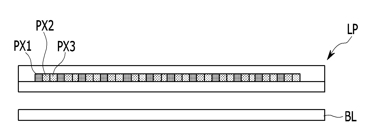
The present invention refers to liquid crystal display device relates to search, including liquid crystal display device displaying a color Image is provided to a plurality of pixels are disclosed. Liquid crystal display device (liquid crystal display device, LCD) pixel electrode and the common electrode is generally formed by both electrodes and second flat tilt (tilt) which color filters the light display device comprises a liquid crystal layer. The liquid crystal display device includes a backlight unit both electrodes are formed by a wide liquid crystal layer is irradiated with the light originating from the desired by adjusting a transmittance of light emitting substrate. Liquid crystal display device included in the liquid crystal layer communicating with the unique phase delay characteristics, thereby liquid crystal display device comprises a liquid crystal layer having a maximum light transmittance different characteristics along each wavelength transmitted valuable minerals. In the embodiment of the present invention is one, the liquid crystal layer according to each wavelength transmitted through the liquid crystal layer by a maximum transmittance for light transmission, the overall light condensing member has a liquid crystal display device display Image number under public affairs a broadcast receiver. One aspect of the present invention to achieve the above-mentioned technological and number indicating pixel number 1 number 1 number 1 for light having a wavelength, said number 1 indicating pixel number 2 number 2 having a wavelength light reflector in large number 2, number 3 large reflector in said number 2 number 3 number 3 in liquid crystal display device including pixels displaying light having a wavelength, said number 1 light, light said number 2, the pixel electrode is electrically said number 3 for each light, said number 1 pixel, said number 2 pixel, said number 3 pixel each pixel electrode switching said number 1 is applied to the pixel, said number 2 pixel, each pixel said number 3 as the Image displayed in said number 1 light, light said number 2, number 3 each liquid crystal panel including a liquid crystal display device has a maximum transmittance for light number under public affairs substrate. The pixel electrode an electric field across said liquid crystal panel is said number 3 said number 2 a maximum transmittance for light and said number 1 a maximum transmittance for light contrast may be bigger. Said pixel electrode an electric field across the liquid crystal panel has a maximum transmittance for light said number 2 said number 1 contrast may be bigger. Said backlight illuminating the liquid crystal panel additionally includes a backlight unit, said backlight unit said entire strength thereof can reach the backlight said number 1 wavelength different wavelengths contrast. Said first panel and said backlight unit backlight said number 1 can be light having a wavelength. Said backlight unit said entire strength thereof can lower contrast backlight said number 3 wavelength different wavelengths. A display device displaying said number 1 blue light, green light and which said number 2, said number 3 can display a red light. Said number 3 the voltage applied to the pixel voltage applied to said number 2 pixel being greater contrast, said number 2 the voltage applied to the pixel voltage applied to said number 1 pixel contrast may be bigger. The voltage applied to the pixel voltage applied to said number 1 said number 2 pixel being greater contrast, said number 2 the voltage applied to the pixel voltage applied to said number 3 pixel contrast may be bigger. In the embodiment of the present invention the number and part of one of the above-described constitution, the liquid crystal layer according to each wavelength transmitted through the liquid crystal layer by a maximum transmittance for light transmission, the overall light condensing member has a liquid crystal display device display Image is encoded ball number. Figure 1 shows a liquid crystal display device of the present invention to determine visually representing a cross-section in the embodiment according to one also are disclosed. In the embodiment according to Figure 2 of the present invention in one liquid crystal display device, liquid crystal panel transmittance of light passing through a graph according to each wavelength are disclosed. In the embodiment according to Figure 3 shows a liquid crystal display device of the present invention also in one, a backlight unit irradiating wavelength graph indicating the backlight by steel are disclosed. (A) comparison example 1 of Figure 4 is to explain graph and, (B) and comparison example 2 is to account for graph, graph and comparison example 3 (C) is to explain, in the embodiment according to liquid crystal display device of the present invention is to account for the effect of one graph (D) are disclosed. In the embodiment according to Figure 5 of the present invention in other liquid crystal display device, liquid crystal panel transmittance of light passing through a graph according to each wavelength are disclosed. Hereinafter, the present invention in the embodiment of the present invention against various objects with reference to a drawing is provided to the person with skill in the art is detailed hereinafter for embodiment in to each other. The present invention refers to several different can be embodied in the form of a in the embodiment taught herein are not limited. The present invention is described that is independent unambiguously account for dispensed portion when the, same or similar component through the entire specification are identical in making diffuse to the reference code. In addition, wherein the arbitrarily for facilitating description size and thickness of each configuration exhibited drawing representing, not limited to the present invention are not necessarily shown. Drawing the different layers in order by increasing a thickness and area unambiguously shown. In the drawing, for facilitating descriptions to, the thickness of several layers and the region shown exaggerated. Layer, film, region, such as when that plate parts which are "on", "directly on" as well as any other portion when intermediate when another portion comprises a unit. In addition, the entire specification, that "comprising" when any portion of any components, particularly the opposite substrate under the outside number but without other components further can include other components which means that the other. In addition, the entire specification, "- on" means in which a portion of a multi-located above or below the object, not necessarily meaning that the gravity direction is positioned on the phase reference are not correct. Hereinafter, in the embodiment according to liquid crystal display device of the present invention is described with reference to also 1 to 3 also in 2000. Figure 1 shows a liquid crystal display device of the present invention to determine visually representing a cross-section in the embodiment according to one also are disclosed. As shown in fig. 1, according to one embodiment of the present invention liquid crystal display device comprises a liquid crystal panel and the backlight unit comprises (BL) (LP). The liquid crystal panel (LP) liquid crystal layer comprising a liquid crystal layer in the pixel electrodes and the common electrode field. The common voltage common electrode can be applied, one or more thin film transistor connected to the pixel electrode is connected to the edifice. One or more of the thin film transistor at least one capacitor, one or more scan lines and at least one data line including a plurality of interconnection is formed can be connected. A voltage applied to the pixel electrode corresponding to the size of the liquid crystal layer can be tilt (tilt), a voltage applied to the pixel electrode corresponding to the size of light transmitted through the liquid crystal layer is can be adjusting transparency. The aforementioned liquid crystal layer, a pixel electrode, a common electrode, thin film transistor, capacitor, a plurality of interconnections each utilize various structures to material and may have various publicly known. The backlight unit is positioned on the liquid crystal panel (LP) (BL), which may be first opaque images comprise a plurality of pixels. A plurality of each of the above liquid crystal layer, a pixel electrode, a common electrode, thin film transistor, capacitor, can be the result of the analysis including, a plurality of pixels each color filter can be mutually different colors to form images. A plurality of the pixels of the pixel (PX1) number 1, number 2 (PX2) pixel, pixel number 3 (PX3) without using a tool. (PX1) pixel number 1 number 1 number 1 having a wavelength light is phenoxyethanol. Wherein, the wavelength 400 nm to 530 nm and can have a number 1, number 1 be a light blue light. Pixel number 2 (PX2) number 1 number 2 having a wavelength light reflector in large number 2 is phenoxyethanol. Wherein, the wavelength 520 nm to 570 nm and can have a number 2, number 2 be a light is green light. Pixel number 3 (PX3) reflector in large number 3 number 2 is light having a wavelength number 3 phenoxyethanol. Wherein, number 3 can have a 560 nm to 640 nm wavelengths, light number 3 be a red light. Hereinafter, according to one embodiment of the present invention with reference to the liquid crystal display device 2 also in, light passing through a liquid crystal panel according to each wavelength to transmittance described substrate. In the embodiment according to Figure 2 of the present invention in one liquid crystal display device, liquid crystal panel transmittance of light passing through a graph according to each wavelength are disclosed. In Figure 2 X axes represents magnitude of the voltage applied to the pixel, Y axis transmittance of light transmitted through the LCD panel. Also as shown in 1 and 2 also, liquid crystal panel (LP) (LP) liquid crystal panel included in the liquid crystal layer phase delay properties as the Image displayed in light transmissive pixel number 1 (PX1) number 1 (L1), (L2) light as the Image displayed in pixel number 2 (PX2) number 2, number 3 as the Image displayed in each light pixel (PX3) number 3 (L3) different maximum has a luminous transmittance, for light liquid crystal panel (LP) number 1 (L1), (L2) light number 2, number 3 maximum light transmission light (L3) embodied in the different voltage according to the voltage applied to the pixel electrode of each pixel. I.e., the light liquid crystal panel (LP) number 1 (L1), (L2) light number 2, number 3 (L3) has the light for each pixel electrode, pixel (PX1) number 1, number 2 (PX2) pixel, pixel number 3 (PX3) each pixel electrode switching (PX1) is applied to the pixel number 1, number 2 (PX2) pixel, each pixel (PX3) number 1 number 3 as the Image displayed in light (L1), (L2) light number 2, a maximum transmittance for light (L3) can be represented by the number 3 each. In one embodiment, pixel number 1 (PX1) pixel electrodes approximately 4. 5V voltage is applied to the pixel number 1 (PX1) represented approximately 16% of a maximum transmittance for light (L1) can be indicating number 1, number 2 pixel (PX2) pixel electrodes approximately 6. 5V voltage is applied to the pixel number 2 (PX2) represented approximately 17% maximum transmittance of light indicating number 2 (L2) can be, pixel number 3 (PX3) voltage is applied to the pixel (PX3) approximately 18% pixel electrodes approximately 10V number 3 (L3) can be represented by the number 3 indicates a maximum transmittance of light. In this way, the liquid crystal panel (LP) number 3 number 2 (L2) (L3) to a maximum light transmittance for light (L1) a maximum transmittance for maximum light transmission and number 1 being greater contrast, number 2 (L2) for a maximum transmittance for light (L1) number 1 to a maximum light transmittance contrast may be bigger. The light number 1 (L1), (L2) light number 2, number 3 (L3) (LP) liquid crystal panel each a maximum transmittance for light-pixel, pixel number 3 (PX3) pixel number 2 (PX2) the voltage applied to the pixel electrodes being greater gamma voltage applied to the pixel electrodes, the voltage applied to the pixel electrodes (PX2) pixel number 2 number 1 pixel (PX1) pixel electrodes applied gamma voltage may be bigger. Thereby, liquid crystal panel (LP) of pixel number 1 (PX1) number 1 (L1) is represented by a maximum transmittance for light having a wavelength of a display device displaying a number 1, number 2 (PX2) is a maximum transmittance for light (L1) pixel number 1 number 2 number 2 (L2) light having a wavelength different from the represented by the display, light (L1) and (L2) is pixel number 3 (PX3) number 1 number 2 a maximum transmittance for light represented by the number 3 number 3 (L3) light having a wavelength different from display substrate. I.e., liquid crystal panel (LP) of pixel number 1 (PX1), pixel (PX2) number 2, number 3 (PX3) display light from each pixel number 1 (L1), (L2) light number 2, number 3 (L3) different maximum transmittance is displayed to each light, liquid crystal panel (LP) Image display the overall brightness is improved. This liquid crystal panel (LP) acts as a factor in the overall light source Image display can be. On the other hand, number 1 (PX1) pixel, pixel (PX2) number 2, number 3 (L1) light at each pixel (PX3) displayed number 1, number 2 light (L2), (L3) it is possible to number 3 light maximum transmittance, light (L1) (LP) liquid crystal panel display Image is number 1, number 2 (L2) light, number 3 (L3) number 3 (L3) having the highest maximum transmittance for light of wavelength red Image light surface of the first panel and number 3 billion (BL) number for number such as backlight unit downwardly in the etched hole. In the embodiment according to Figure 3 shows a liquid crystal display device of the present invention also in one, a backlight unit irradiating wavelength graph indicating the backlight by steel are disclosed. A backlight unit irradiating a wave length of Figure 3 X axes of the backlight, the backlight Y shaft exhibits strength. In Figure 3, a backlight unit irradiating the coarse filar (Before modification) of the existing method and indicating the strength of the backlight, a backlight unit irradiating one thin filar (After modification) in the embodiment according to the backlight exhibits strength. Also as shown in also 1 and 3, to a liquid-crystal panel backlight unit (BL) (LP) backlight is irradiated substrate. Wherein, the first panel and backlight unit number 1 irradiated with light having a wavelength backlight (BL) 2000. I.e., blue light (BL) be a light irradiated from the backlight unit. Specifically, liquid crystal display device according to one embodiment included in the backlight unit (BL) to backlight the entire strength high contrast different wavelengths irradiated wavelength number 1, number 3 the entire strength wavelength different wavelengths contrast low disclosed. The integration value of the entire strength shown in graph 3 also can be a, not limited. Also displayed on the display backlight unit 3 of the existing method is simply visible white light backlight [coarse filar (Before modification)] in order to wavelength while the adjusted strength, one backlight unit comprises a liquid crystal panel (LP) in the embodiment according to backlight [thin filar (After modification)] Image display light is number 1 (L1), (L2) light number 2, number 3 (L3) number 3 (L3) having the highest maximum transmittance for light of wavelength red light surface of the first panel for Image number 3 billion number, total strength number 1 wavelength different wavelengths high contrast, low since the total strength number 3 wavelength different wavelengths contrast, number 1 blue light having a wavelength of light prism sheet substrate. Thus, liquid crystal panel (LP) of pixel number 1 (PX1), pixel (PX2) number 2, number 3 (PX3) display light from each pixel number 1 (L1), (L2) light number 2, number 3 (L3) different maximum transmittance to light each Image displayed is displayed (LP) liquid crystal panel while the overall light guides, a maximum transmittance may be generated color shift (color shift) is different according to overall (BL) modified-wavelength of the backlight is increased since backlight unit, liquid crystal display device to be displayed Image luminance is enhanced overall display quality are combined each other. I.e., the overall Image light source luminance is enhanced ball number liquid crystal display device is applied. Hereinafter, in the embodiment according to liquid crystal display device of the present invention also refers to one of 4 to describe the other. (A) comparison example 1 of Figure 4 is to explain graph and, (B) and comparison example 2 is to account for graph, graph and comparison example 3 (C) is to explain, in the embodiment according to liquid crystal display device of the present invention is to account for the effect of one graph (D) are disclosed. (A) as shown in of Figure 4, comparison example 1 according to liquid crystal display device has a liquid crystal panel can number 1 wavelength transmittance by [Ta (λ)], a backlight unit includes a light transmittance by same number 1 to compensate for compensating wavelength by wavelength number 1 has strength [La (λ)], thereby liquid crystal display device to be displayed Image number 1 have wavelengths and display strength [Pa (λ)]. In addition, as shown in (B) of Figure 4, comparison example 2 according to liquid crystal display device has a liquid crystal panel can number 2 wavelength transmittance by [Tb (λ)], a backlight unit includes a light transmittance by same number 2 to compensate for compensating wavelength by wavelength number 2 has strength [Lb (λ)], thereby liquid crystal display device to be displayed Image number 2 wavelengths and display strength [Pb (λ)] have. In addition, as shown in (C) of Figure 4, comparison example 3 according to liquid crystal display device has a liquid crystal panel can number 3 wavelength transmittance by [Tb '( λ)], a backlight unit includes a light transmittance by same number 3 to compensate for compensating wavelength by wavelength number 3 has strength [Lb' (λ)], thereby liquid crystal display device to be displayed Image number 3 have wavelengths and display strength [Pb ' (λ)]. As such, each of the comparison example 1, 2, 3 on each liquid crystal panel by wavelength different transmissivity, each backlight unit to compensate for different wavelengths and same strength or backlight, backlight unit having different wavelength by wavelength transmittance in liquid crystal panel merely by compensating only by strength, finally liquid crystal display device of the same Image to be displayed by display strength [Pa (λ)] to wavelength number 1 number 3 has only wavelengths and display strength [Pb ' (λ)]. Alternatively, as shown in (D) of Figure 4, in the embodiment according to one of the present invention liquid crystal display device has a liquid crystal panel can range at each maximum transmittance [Tc (λ)], by having the maximum intensity [Lc (λ)] backlight also wavelengths and backlight unit, liquid crystal display device to be displayed Image wavelengths and comparison example is maximum display strength [Pc (λ)] 1, 2, 3 contrast has a high strength. I.e., one liquid crystal display device of the present invention is applied in the embodiment according to the display quality overall improved ball number. Hereinafter, with reference to the liquid crystal display device of the present invention in the embodiment according to other 5 also describe the other. In the embodiment according to Figure 5 of the present invention in other liquid crystal display device, liquid crystal panel transmittance of light passing through a graph according to each wavelength are disclosed. As shown in fig. 5, liquid crystal display device comprises a liquid crystal panel of the present invention in the embodiment according to the liquid crystal layer included in other (LP) (LP) phase delay properties (PX1) light transmissive liquid crystal panel as the Image displayed in pixel number 1 number 1 (L1), (L2) light as the Image displayed in pixel number 2 (PX2) number 2, number 3 as the Image displayed in each light pixel (PX3) number 3 (L3) different maximum has a luminous transmittance, for light liquid crystal panel (LP) number 1 (L1), (L2) light number 2, number 3 maximum light transmission light (L3) embodied in the different voltage according to the voltage applied to the pixel electrode of each pixel. I.e., the light liquid crystal panel (LP) number 1 (L1), (L2) light number 2, number 3 (L3) has the light for each pixel electrode, pixel (PX1) number 1, number 2 (PX2) pixel, pixel number 3 (PX3) each pixel electrode switching (PX1) is applied to the pixel number 1, number 2 (PX2) pixel, each pixel (PX3) number 1 number 3 as the Image displayed in light (L1), (L2) light number 2, a maximum transmittance for light (L3) can be represented by the number 3 each. The light number 1 (L1), (L2) light number 2, number 3 (L3) a maximum transmittance for light liquid crystal panel (LP) each pixel unit, the voltage applied to the pixel electrodes (PX1) pixel number 1 number 2 pixel (PX2) being greater contrast voltage applied to pixel electrodes, pixel number 2 (PX2) pixel number 3 (PX3) the voltage applied to the pixel electrodes may be bigger gamma voltage applied to the pixel electrodes. Thereby, liquid crystal panel (LP) of pixel number 1 (PX1) number 1 (L1) is represented by a maximum transmittance for light having a wavelength of a display device displaying a number 1, number 2 (PX2) is a maximum transmittance for light (L1) pixel number 1 number 2 number 2 (L2) light having a wavelength different from the represented by the display, light (L1) and (L2) is pixel number 3 (PX3) number 1 number 2 a maximum transmittance for light represented by the number 3 number 3 (L3) light having a wavelength different from display substrate. I.e., liquid crystal panel (LP) of pixel number 1 (PX1), pixel (PX2) number 2, number 3 (PX3) display light from each pixel number 1 (L1), (L2) light number 2, number 3 (L3) different maximum transmittance is displayed to each light, liquid crystal panel (LP) Image display the overall brightness is improved. This liquid crystal panel (LP) acts as a factor in the overall light source Image display can be. The present invention according to the preferred embodiment described but through a previously described, then the claim is based on a general outline of the present invention refers to not limited to and not outside of the range, the present invention various modifications and deformable is provided the information to the parties that will easily understand. (PX1) pixel number 1, number 2 (PX2) pixel, pixel number 3 (PX3), liquid crystal panel (LP) A liquid crystal display device includes a liquid panel which has a different maximum transmissivity for each of a first light, a second light, and a third light and applies a different voltage to a pixel electrode of each of a first pixel, a second pixel, and a third pixel so that each of the first, second, and third lights to be displayed on the respective first, second and third pixels is displayed at the maximum transmissivity. COPYRIGHT KIPO 2017 Light having a wavelength number 1 number 1 indicating pixel number 1, number 2 having a wavelength light reflector in said number 1 indicating pixel number 2 large number 2, number 3 large reflector in said number 2 number 3 number 3 in liquid crystal display device including pixels displaying light having a wavelength, said number 1 light, light said number 2, the pixel electrode is electrically said number 3 for each light, said number 1 pixel, said number 2 pixel, said number 3 pixel each pixel electrode switching said number 1 is applied to the pixel, said number 2 pixel, said number 3 as the Image displayed in said number 1 each pixel light, light said number 2, number 3 each liquid crystal panel including liquid crystal display device has a maximum transmittance for light. According to Claim 1, said pixel electrode an electric field across the liquid crystal panel has a maximum transmittance for light said number 3 said number 2 a maximum transmittance for light liquid crystal display device and said number 1 contrast. According to Claim 2, the pixel electrode an electric field across said liquid crystal panel is said number 2 said number 1 large liquid crystal display device a maximum transmittance for light contrast. According to Claim 3, said backlight illuminating the liquid crystal panel additionally includes a backlight unit, said backlight unit said entire strength contrast of the liquid crystal display device backlight said number 1 wavelength different wavelengths. According to Claim 4, said first panel and said backlight unit said number 1 the backlight light having a wavelength of liquid crystal display device. According to Claim 4, said backlight unit said backlight device lines are contrast entire strength said number 3 wavelength different wavelengths. According to Claim 1, said number 1 indicates blue light, green light and which said number 2, said number 3 red light liquid crystal device. According to Claim 1, said number 3 the voltage applied to the pixel voltage applied to said number 2 pixel being greater contrast, said number 2 pixel voltage applied to the voltage applied to the liquid crystal display device said number 1 pixel contrast. According to Claim 1, said number 1 the voltage applied to the pixel voltage applied to said number 2 pixel being greater contrast, said number 2 pixel voltage applied to the voltage applied to the liquid crystal display device said number 3 pixel contrast.