3D TOUCH SENSOR AND MANUFACTURING METHOD THEREOF
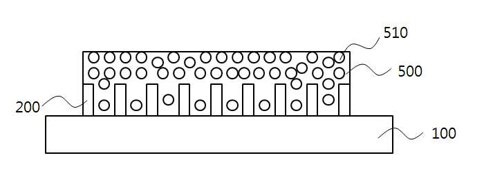
The present invention refers to 3 dimensional touch sensor and the number of bath method are disclosed. Touch-entry is next generation input manner to penetrate through the data to the electronic device without an attempt are more various touch input and reduces, the applicable to a wide variety of environments for enabling recognition of the touch sensor touch the correct development studies has been also reduces disclosed. This touch input technology is considerably resistor film and method for monitoring capacitance can be. First, resistor film has upper and lower electrode film are spaced apart by a spacer, caused forms a arranged so as to contact each other, the upper electrode film is formed on the top plate finger, between the upper and lower electrode film is pressed by means of an input pen electrical, resistance value change according to its position coordinates a voice control unit number voltage variations in such a way that contact are disclosed. On the other hand, for capacitive again to classification for capacitive (Surface Capacitive) projected surface for capacitive (Projected Capacitive) can be. For capacitive metal edge pattern ITO layer of a flat surface, said ITO layer formed magnetic field throughout the finger screen in which the change of capacity of four-dimensional extracting corner detection scheme is disclosed. The first transparent electrode for capacitive projection formed according to variations in capacitance is provided by each channel longitudinal axis and a transverse axis and a longitudinal axis axis in such a way that extracting position coordinates are disclosed. The touch sensor Z axis direction in addition to a dielectric layer can be 3 dimensional touch techniques know pressure is introduced into the disclosed. However, conventional touch input technique is multi-touch bottom face to make it difficult, interference between the three air sensing becomes difficult, X, Y axis position detection additionally Z axis makes a door number response sensitive to pressure applied flow tides. The touch screen is capable of processing 3 dimensional signal related publicized patent number 2010 - 0004324 Korean disclosure but, when the aforementioned door number alternative point number was inaccurate. The present invention refers to 3 dimensional touch sensor capable of improving the transmittance number 3 dimensional touch sensor under public affairs intended. The present invention refers to 3 dimensional touch sensor capable of improving the sensitivity of the intended number under public affairs 3 dimensional touch sensor. The present invention refers to said 3 dimensional touch sensor intended for a number the number under public affairs bath method. 1. Said substrate and formed on the transparent electrode including conductive nano partition; and Said transparent electrode on one side of the transparent dielectric layer; a including 3 dimensional touch sensor. 2. In on 1, 5 to 200 nm thickness in said compartment provides a nano, 3 dimensional touch sensor. 3. In over 1, the partition is formed a predetermined pattern said nano, 3 dimensional touch sensor. 4. In on 3, said pattern openings are won, oval, triangular, rectangular, five rectangularities, hexagon, or octagon shape mixed figure opening pattern, 3 dimensional touch sensor. 5. In 1 above, wherein the substrate is at least a part connected to one another on the substrate between the partition and the partition said nano, 3 dimensional touch sensor. 6. In over 1, said nano is from 50 to 2,000 nm in, 3 dimensional touch sensor. 7. In over 1, said compartment provides a nano In, Co, Si, Ge, Au, Pd, Pt, Ru, Re, Mg, Zn, Hf, Ta, Rh, Ir, W, Ti, Ag, Cr, Mo, Nb, Al, Ni, Cu, and consisting of at least one metal selected from the group consisting 1 WTi; or indium composition for producing cable (ITO), indium gong [khu[khu] oxide (IZO), indium gong [khu[khu] oxide (IZTO), aluminum gong [khu[khu] oxide (AZO), gallium gong [khu[khu] oxide (GZO), polyarylene ether sulfone for producing cable (FTO), the indium composition for producing cable (ITO-a Ag a-ITO) indium composition for producing cable - -, - - gong [khu[khu] oxidegong [khu[khu] oxide indium is indium (IZO provided Ag provided IZO), indium and aluminum indium gong [khu[khu] oxidegong [khu[khu] oxide - - - - the aging [...] some silkgong [khu[khu] oxide (IZTO provided Ag provided IZTO) is at least one selected from the group consisting of aluminum (AZO provided Ag provided AZO) 1 including a non-metal oxide as a by-product, 3 dimensional touch sensor. 8. In over 1, said transparent dielectric layer covering said conductive nano separation wall openings, 3 dimensional touch sensor. 9. In over 1, said transparent dielectric layer including conductive particles, 3 dimensional touch sensor. 10. In the Kr-doped tin oxide (tin oxide) 9 on said conductive particles, metal nanowires and carbon nano wire is at least one selected from the group consisting, 3 dimensional touch sensor. 11. In on 9, said transparent dielectric layer said conductive particle density including a plurality of layers different, 3 dimensional touch sensor. 12. In on 11, said transparent dielectric layer applied to the layer of conductive particle density side pressure higher, 3 dimensional touch sensor. 13. In 1 above, further including at least a portion of polymer pattern between the partition said conductive nano, 3 dimensional touch sensor. 14. In over 1, said transparent electrodes are formed along said number 1 and number 2 number 1 number 1 sensing electrodes insulated from sensing electrodes in at least one of sensing electrodes formed along number 2, 3 dimensional touch sensor. 15. In over 14, said number 1 and number 2 the sensing electrodes sensing electrodes formed on the same substrate, 3 dimensional touch sensor. 16. 1 to 15 of 3 dimensional touch sensor including on touch screen panel. 17. Forming a conductive layer on a substrate; Said forming a polymer pattern over the conductive layer; The exposed conductive layer and an ion milling etching said pattern, said pattern is prepared by forming a barrier polymer nano thickness supports; and Said nano separation wall transparent dielectric layer formed on a substrate; Including a, 3 dimensional touch sensor number bath method. 18. Forming a polymer pattern on a substrate; Said polymer pattern formed on the substrate on which conductive layer; An ion milling etching said conductive layer, said polymer pattern prepared by forming a side of the inner side of barrier rib supports; and Said nano separation wall transparent dielectric layer formed on a substrate; Including a, 3 dimensional touch sensor number bath method. 19. In on 17 or 18, said partition wall has a thickness of 5 to 200 nm in nano, 3 dimensional touch sensor number bath method. 20. In on 17 or 18, said polymer pattern is formed into nano the printing law being, 3 dimensional touch sensor number bath method. 21. In 17 or 18 above, conductive particles to said coating layer ion milling tearing out, wash-off attached to the polymer pattern formed by, 3 dimensional touch sensor number bath method. 22. In on 17 or 18, said conductive layer In, Co, Si, Ge, Au, Pd, Pt, Ru, Re, Mg, Zn, Hf, Ta, Rh, Ir, W, Ti, Ag, Cr, Mo, Nb, Al, Ni, Cu, and consisting of at least one metal selected from the group consisting 1 WTi; or indium composition for producing cable (ITO), indium gong [khu[khu] oxide (IZO), indium gong [khu[khu] oxide (IZTO), aluminum gong [khu[khu] oxide (AZO), gallium gong [khu[khu] oxide (GZO), polyarylene ether sulfone for producing cable (FTO), the indium composition for producing cable (ITO-a Ag a-ITO) indium composition for producing cable - -, - - gong [khu[khu] oxidegong [khu[khu] oxide indium is indium (IZO provided Ag provided IZO), indium and aluminum gong [khu[khu] oxide - - - - the indium gong [khu[khu] oxidegong [khu[khu] oxide (IZTO provided Ag provided IZTO) is at least one selected from the group consisting of aluminum gong [khu[khu] oxide (AZO provided Ag provided AZO) 1 including a non-metal oxide as a by-product, 3 dimensional touch sensor number bath method. 23. In on 17 or 18, said ion milling is 10-5 Torr to 10-3 Torr to accelerating plasma is carried out to a pressure of at 100ev 1500eV, 3 dimensional touch sensor number bath method. 24. In on 17 or 18, further including a stand-alone said polymer pattern number, 3 dimensional touch sensor number bath method. 25. In on 17 or 18, said transparent dielectric layer including conductive particles, 3 dimensional touch sensor number bath method. 26. In on 17 or 18, wherein the transparent dielectric layer said conductive particles having a layer of a different, 3 dimensional touch sensor number bath method. 27. In over 26, said transparent dielectric layer applied to the layer of conductive particle density formed higher pressure side, 3 dimensional touch sensor number bath method. The touch sensor of the present invention 3 dimensional conductive nano partition, 3 dimensional touch sensor transmittance can be significantly. A transparent electrode on one side of the transparent dielectric layer of the present invention 3 dimensional touch sensor including, Z axis in response to sensitivity can be significantly sensitive to pressure applied. In one embodiment of the present invention is used in 1 to 4 also according to 3 dimensional touch sensor with coarse perspective view are disclosed. 5 and 6 respectively of the present invention in one embodiment according to 3 dimensional touch sensor number bath method also of coarse standpoint are disclosed. Figure 7 shows a schematic diagram of the operation of the implementation of the present invention is to produce a shape according to 3 dimensional touch sensor also are disclosed. The present invention refers to said substrate and formed on the transparent electrode including conductive nano partition; and said transparent electrode on one side of the transparent dielectric layer; thereby, as well as minimizes applied to transmittance 3 dimensional touch sensor, sensitive to pressure applied Z axis in response to a 3 dimensional touch sensor and method for improving sensitivity of the number tank are disclosed. Hereinafter, with reference to the drawing of the present invention specific embodiment form produced in less than 1000. But, the next drawing are appended to the specification of the present invention preferred one embodiment example in which, further understanding of the invention the video and feature of the present invention which serves the aforementioned three, in the present invention refers to a confined only to the interpreted to such drawing like a WD other. As shown in fig. 1 of the present invention 3 dimensional touch sensor, substrate (100) and said substrate (100) which is located on the conductive nano partition (200) including a transparent electrode; and said transparent electrode on one side of the transparent dielectric layer (500) comprises. Substrate (100) having proper strength if this resin does not specifically defined, such as silicone, quartz, glass, polymer, metal, metal oxide, non-metallic oxide, such as norbornene or polycyclic norbornene monomer including a cycloolefin monomer unit having a cycloolefin-based derivatives, diacetyl cellulose, triacetyl cellulose, acetyl cellulose butyl rate, isobutyl ester cellulose, propionyl cellulose, butyrolactone pro blood Oniel cellulosereel cellulose or acetyl cellulose in NaCl, ethylene - vinyl acetate copolymer, polyester, polystyrene, polyamide, polyether-imide, polyacrylamide, polyimide, polyether sulfone, polysulfone, polyethylene, polypropylene, poly methylpentene, polyvinyl chloride, poly vinylidene chloride, polyvinyl alcohol, polyvinyl acetal, polyether ketone, polyether ether ketone, polyether sulfone, slurry by, polyethylene terephthalate, polybutylene terephthalate, polyethylene naphthalate, polycarbonate, polyurethane, epoxy substrate (100) including a front end equipped 99900 00327999 implementation being. These materials can be mixed alone or in combination with at least one 2. Substrate (100) has a thickness of not specifically defined, for example 10 to 500 micro m implementation being. As shown in fig. 2, conductive nano partition (200) substrate (100) positioned on, the present invention according to the partition at the nano level heaters are formed nano means other. The touch sensor of the present invention 3 dimensional X, Y axis direction sensing electrodes is formed is injected into the first panel nano sensing electrodes not significantly improved transmittance...copyright 2001. Conductive nano partition (200) is prepared by the number conductive material, for example In, Co, Si, Ge, Au, Pd, Pt, Ru, Re, Mg, Zn, Hf, Ta, Rh, Ir, W, Ti, Ag, Cr, Mo, Nb, Al, Ni, Cu, and consisting of at least one metal selected from the group consisting 1 WTi; or indium composition for producing cable (ITO), indium gong [khu[khu] oxide (IZO), indium gong [khu[khu] oxide (IZTO), aluminum gong [khu[khu] oxide (AZO), gallium gong [khu[khu] oxide (GZO), polyarylene ether sulfone for producing cable (FTO), the indium composition for producing cable (ITO-a Ag a-ITO) indium composition for producing cable - -, - - gong [khu[khu] oxidegong [khu[khu] oxide indium is indium (IZO provided Ag provided IZO), the indium gong [khu[khu] oxide - 999 0000398999 gong [khu[khu] oxidegong [khu[khu] oxide - aluminum and aluminum indium (IZTO provided Ag provided IZTO) is selected from the group consisting of 1 - gong [khu[khu] oxide (AZO provided Ag provided AZO) at least one metal oxide or the like can be used. The partition wall nano sensitivity improvement effect can be achieved within a range to minimize the degradation in the transmittance and if not specifically defined, and may be 5 to 200 nm thickness for example then, preferably 5 to 100 nm, more preferably 5 to 50 nm, most preferably 10 to 30 nm implementation being. There may be a door number and thickness is below conductive and endurance is 5 nm, 200 nm can be greater than the pressure drop. Nano height may indicate if sufficient sensitivity and light transmittance within a range not specifically defined, for example 50 nm to 2,000 nm implementation being. The degree of sensitivity can be insignificantly height is below 50 nm, greater than 2,000 nm excessive deterioration of the durability of the presence of the gap 3 dimensional touch sensor can be door number is generated. Nano partition (200) alone or a plurality of wall can be located. A plurality of wall when positioned parallel, nano partition (200) does not variable are specially defined, for example 10 nm to 3 may be micro m, preferably 10 to 200 nm in terms of improving light extraction efficiency implementation being. A plurality of wall without parallel, or meet each other, the extended line positioned to meet each other disapproval. The interval of the nano partition does not specifically defined, for example 10 nm to 3 may be micro m, preferably 10 to 200 nm in terms of improving light extraction efficiency implementation being. Nano 3 as at least a part between the partition also illustrated compartment provides a substrate (100) may be connected to one another on. They are sensitivity can be improved more. (F) 5 also hexagonal opening apart on the substrate between at least a part of the partition wall opening even nano when connected to one another is shown disclosed. Nano compartment provides a predetermined pattern the Optocomponents. For example opening as a pattern, won opening, oval, triangular, rectangular, five rectangularities, hexagonal, polygonal such as octagon, or can be combined with shape, linear pattern, a mesh pattern, zigzag, helical, radiation type, irregular shape such as a single sum may have disclosed. 4 hexagonal opening is an opening pattern but also plate is illustrated, the one number are not disclosed. While partition opening pattern as a pattern having an opening surrounded into nano, alone or in combination with an opening pattern for the plurality can be positioned. When a plurality of opening patterns is located, each aperture pattern of regularly or irregularly intervals can be located. In addition, a plurality of opening patterns are connected to each other or can be spaced apart from, axisymmetric, point-symmetrical or irregular can be positioned. The illustrated figure shape pattern for said opening; said combined with the illustrated figure shape; or may have at least one or more figure 1 is mixed shape as, opening periodically, aperiodically over a can be arranged. Not specifically defined with an aperture, for example the length of 100 nm to 1 micro m long implementation being. Of the present invention 3 dimensional touch sensor with transparent electrodes are conductive nano partition (200) between at least a portion of polymer pattern (420) can be further. Polymer pattern (420) if it was found using publicly known polymer resin grudge without number it transparent polymer can be, for example epoxy, cellulosic, acrylic, vinyl chloride, vinyl acetic acid, polyvinyl alcohol, polyurethane, be a polymer resin such as polyester. They can be mixed alone or in combination with at least one 2. In addition, as shown in fig. 1 according to 3 dimensional touch sensor of the present invention in one embodiment, substrate and said transparent electrode located on one side of the transparent dielectric layer including conductive nano partition (500) comprises. Transparent dielectric layer (500) is in the range of mops can be publicly known one special number is cannot be formed, for example, binder and conductive particles (510) can be a. The Z axis can be applied to sense pressure resilient transparent by including a dielectric layer including conductive particles, Z-axis direction can be further improving touch sensitivity. In one embodiment of the present invention is also 7 when pressure is applied to the touch sensor according to 3 dimensional, conductive particles (510) surface of the and density varying coarse form is shown disclosed. Conductive particles (510) surface of the and density changes in capacitance along Z-axis direction to change a specified point can touch recognition. Mops and publicly known binder can be used without a special number of redundant rows or columns, for example, Poly (3, 4 a-ethylenedbxythbphene) poly (styrenesulfonate) (PEDOT/PSS) can be using. Special number has a conductive elastic and conductive particles can be used but if grudge without, for example Kr-doped tin oxide (tin oxide), metal nanowires and carbon nano wires is cited. They can be mixed alone or in combination with at least one 2. Kr-doped tin oxide (tin oxide) is can be spherical, or complex electrical and mechanical properties can be shaped. For example, an electrical sensitivity field - in order to increase the pressure applied to the auxiliary electron tunneling (field a-assisted electron tunnelling) (acicular) particles for promoting the needle shape can be. More particularly is used for supporting, -doped tin oxide (tin oxide) needle particles spherical particles (e.g., needle-shaped particles having an aspect ratio greater than 1:1) can be a mixture of. Selection of a number of spherical particles in a specific proportion to needle pressure sensitivity can be selected according to the final article. In addition, conductive particles does not metal are specially defined metal nanowires, for example the (Ag), gold, aluminum, copper, iron, nickel, titanium, [theyl[theyl] Rhenium, such as chromium is cited. They can be mixed alone or in combination with at least one 2. If necessary, further comprise transparent dielectric layer dielectric filler may be filled. Dielectric filler be a fumed silica or other dielectric particles. Optical properties of composite dielectric particles in small amounts can be further for maintaining, or changing an optical property contains can be further. Dielectric particles by adding an resistance force (resistance-a force) can be alter - response. Preferably, as shown in fig. 1 of the present invention another example implementation according to 3 dimensional touch sensor, comprising a plurality of layers different transparent dielectric layer conductive particle density can be, more specifically includes a P-side transparent dielectric layer layer by forming higher density of conductive particles, conductive particles of sensitive deformation upon application pressure to further improve touch sensitivity capable of Z-axis direction. In addition, sensing electrodes of the present invention 3 dimensional touch sensor with transparent electrodes are formed along number 1 number 1 and number 2 sensing electrodes insulated from said number 1 number 2 can be formed along at least one of sensing electrodes. Thus, the present invention according to at least one of the transparent electrode layer is formed number 1 and number 2 sensing electrodes sensing electrodes effect can be displayed. In the present invention according to one in the embodiment, sensing electrodes each other said number 1 and number 2 the sensing electrodes can be formed on the substrate, 3 dimensional touch sensor of the present invention 3 dimensional touch sensor includes when applied to conventional configuration can be further required. In the embodiment in the present invention according to other, said number 1 and number 2 the sensing electrodes can be formed on the same substrate sensing electrodes, number 1 and number 2 of the present invention 3 dimensional touch sensor includes sensing electrodes electrically insulated from each other electrode measures with insulating layers, number 1 or number 2 sensing electrodes electrically interconnecting bridge (connecting electrodes) 3 dimensional touch sensor electrode measures such as when applied to conventional configuration can be further required. In addition, the present invention refers to said 3 dimensional touch sensor including touch screen panel number under public affairs substrate. The present invention according to 3 dimensional touch sensor configuration except that the mops are combined to form a touch screen panel can be publicly known. In addition, the present invention refers to said 3 dimensional touch sensor with a number bath method number under public affairs substrate. Hereinafter of the present invention in one embodiment according to 3 dimensional touch sensor number bath method are described substrate. First, (b) also 5 such as substrate (100) on a conductive layer (300) formed on the substrate. Conductive layer (300) forming method is not specifically defined, physical vapor deposition, chemical vapor deposition, plasma deposition, plasma polymerization process, thermal deposition method, a thermal oxidation method, by using an anodizing process, cluster ion-beam deposition, screen printing, gravure printing, flexographic printing, offset printing, inkjet coating, dispenser printing, such as it was found by a photolithography method can be publicly known. Conductive layer (300) conductive material is preferably used for example In, Co, Si, Ge, Au, Pd, Pt, Ru, Re, Mg, Zn, Hf, Ta, Rh, Ir, W, Ti, Ag, Cr, Mo, Nb, Al, Ni, Cu, and consisting of at least one metal selected from the group consisting 1 WTi; or indium composition for producing cable (ITO), indium gong [khu[khu] oxide (IZO), indium gong [khu[khu] oxide (IZTO), aluminum gong [khu[khu] oxide (AZO), gallium gong [khu[khu] oxide (GZO), polyarylene ether sulfone for producing cable (FTO), the indium composition for producing cable (ITO-a Ag a-ITO) indium composition for producing cable - -, - - gong [khu[khu] oxidegong [khu[khu] oxide indium is indium (IZO provided Ag provided IZO), the indium gong [khu[khu] oxide - - - - aluminum gong [khu[khu] oxidegong [khu[khu] oxide[...] ∴ [...]pettysilk (IZTO provided Ag provided IZTO) and aluminum is made of at least one selected from the group consisting 1 (AZO provided Ag provided AZO) but using metal oxide or the like, the number one are not disclosed. Polymer pattern (420) before a conductive layer (300) when using the first photoresist pattern, polymer pattern (420) to a conductive layer (300) is present. In such a case the after alcoholic beverage it will do partition the nanotubes that are formed by a conductive layer (300) exists, e.g. nano conductive layer (300) on a substrate by (100) connected to one another on to be coated. The, electric conductivity and sensitivity can be improved. After, also 5 (c), (d) said such as conductive layer (300) on polymer pattern (420) formed on the substrate. Polymer pattern (420) conductive layer (300) on polymer resin layer (410) is formed, anti-reflective coating can be same. Polymer pattern is removed along the height of the nano, polymer pattern of the present invention can be selected to adjust the height of the nano height. Polymer resin layer (410) using publicly known polymer resin can be grudge without number provided it was found, for example epoxy, cellulosic, acrylic, vinyl chloride, vinyl acetic acid, polyvinyl alcohol, polyurethane, be a polymer resin such as polyester. They can be mixed alone or in combination with at least one 2. Polymer resin layer (410) of e-beam exposure method are specially without limit for example screen-printing, gravure printing, flexographic printing, offset printing, inkjet coating, dispenser printing, photolithography, such as using nano-imprinting method can be, transmittance to further improve and sensitivity can be can be in one aspect preferably by nano in the printing law being. An opening pattern defined by partition and bulkheads determined. plaque turning conductive layer (300) to etching of the insulating layer for patterning portion of hereinafter (300) can be performed to expose. After, said pattern (e) also 5 such as exposed conductive layer (300) and an ion milling etching, said polymer pattern (420) side supports and nano thickness prepared by partition (200) formed on the substrate. Ion milling technique is by radiating an ion beam conductive layer (300) is physically etching method, a voltage difference between the ion conductive layer accelerate (300) to physical shocking the substrate. The metal particles are out polymer pattern tearing out, (420) is attached to the, polymer pattern (420) can be nano thickness of coating layer. Nano thickness coating layer nano partition (200) corresponding to each other. For example argon ion for forming gas, helium, nitrogen, hydrogen, oxygen or a combination of red may be gas, preferably argon can be. Ion milling conditions not specifically defined, for example 10-5 Torr to 10-3 Torr a pressure of at gas formed plasma, plasma can be accelerated to 100eV - 1500eV widthwise. Energy less than 100eV conductivity layer (300) may be difficult for etching, the polymer pattern greater than 1500eV (420) is difficult to be produced to form nano partition. Nano partition (200) can be achieved within a range to minimize the thickness of the light shielding effect and sensitivity if not specifically defined, for example thickness may be 5 to 200 nm, preferably 5 to 100 nm, more preferably 5 to 50 nm, most preferably 10 to 30 nm implementation being. There may be a door number and thickness is below conductive and endurance is 5 nm, 200 nm can be greater than the pressure drop. Nano partition (200) which can effect sufficient sensitivity and sensitivity in the height of the if not specifically defined, for example 50 nm to 2,000 nm implementation being. The degree of sensitivity can be insignificantly thickness is below 50 nm, greater than 2,000 nm excessive deterioration of the durability of the presence of the gap 3 dimensional touch sensor can be door number is generated. Nano partition (200) does not specifically defined the distance of, for example 10 nm to 3 may be micro m, preferably 10 to 200 nm in terms of transmission and sensitivity implementation being. Next, nano separation wall substrate (100) on the center of the dielectric layer (not shown) formed on the substrate. A transparent dielectric layer are formed using a special number grudge without mops and publicly known back method can be, for example the aforementioned conductive particles including curing/drying formed binder solution but, limited to are not correct. Transparent dielectric layer can be conductive particle, can be conductive particles comprises the above-described conductive particles. In addition, the method of the present invention another example implementation according to 3 dimensional touch sensor number tank, transparent dielectric layer can form a plurality of layers having different density of conductive particles, more specifically by forming a layer of conductive particle density higher pressure applied side, conductive particles of sensitive deformation upon application pressure to further improve touch sensitivity capable of Z-axis direction. If necessary, the method of the present invention 3 dimensional touch sensor number bath (f) also 5 such as said polymer pattern (420) further include the step of a number can be industry. In addition, the present invention refers to a method according to 3 dimensional touch sensor with another implementation number tank number under public affairs substrate. Hereinafter, another implementation according to 3 dimensional touch sensor number bath method are described substrate. First, also 6 (a) as the substrate (100) on polymer pattern (420) formed on the substrate. Polymer pattern (420) substrate (100) on polymer resin layer is formed, anti-reflective coating can be same. Polymer resin layer is formed on the it was found using publicly known polymer resin grudge without number can be, for example epoxy, cellulosic, acrylic, vinyl chloride, vinyl acetic acid, polyvinyl alcohol, polyurethane, be a polymer resin such as polyester. They can be mixed alone or in combination with at least one 2. Polymer resin layer patterning method are specially without limit for example screen-printing, gravure printing, flexographic printing, offset printing, inkjet coating, dispenser printing, photolithography, such as using nano-imprinting method can be, transmittance to further improve and sensitivity can be can be in one aspect preferably by nano in the printing law being. After, 6 (b) also leaves said polymer pattern (420) are formed (100) on a conductive layer (300) formed on the substrate. Conductive layer (300) at least one ferritic 1 metal, 1 of at least one metal oxide conductive material, physical vapor deposition, chemical vapor deposition, plasma deposition, plasma polymerization process, thermal deposition method, a thermal oxidation method, by using an anodizing process, cluster ion-beam deposition, screen printing, gravure printing, flexographic printing, offset printing, inkjet coating, dispenser printing, such as photolithography method it can be formed, the one number are not disclosed. After, 6 (c) also leaves said conductive layer (300) and an ion milling etching, said polymer pattern (420) side supports and nano thickness prepared by partition (200) formed on the substrate. For example argon ion for forming gas, helium, nitrogen, hydrogen, oxygen or a combination of red may be gas, preferably argon can be. Ion milling conditions not specifically defined, for example 10-3 To 10 mTorr-5 Formed mTorr a pressure of at gas plasma, plasma can be accelerated to 100eV - 1500eV widthwise. Energy less than 100eV conductivity layer (300) may be difficult for etching, the polymer pattern greater than 1500eV (420) is difficult to be produced to form nano partition. Nano partition (200) minimizing the thickness of the sensibility improvement effect and the degradation in the transmittance can be achieved if not specifically defined within which, for example may be 5 to 200 nm, preferably 5 to 100 nm, more preferably 5 to 50 nm, most preferably 10 to 30 nm implementation being. There may be a door number and thickness is below conductive and endurance is 5 nm, 200 nm can be greater than the pressure drop. Nano partition (200) may exhibit sufficient sensitivity and the height of the light transmittance within a range not specifically defined if, for example 50 nm to 2,000 nm implementation being. The degree of sensitivity can be insignificantly thickness is below 50 nm, greater than 2,000 nm excessive deterioration of the durability of the presence of the gap 3 dimensional touch sensor can be door number is generated. Nano partition (200) does not specifically defined the distance of, for example 10 nm to 3 may be micro m, preferably 10 to 200 nm in terms of transmission and sensitivity implementation being. If necessary, the method of the present invention 3 dimensional touch sensor number bath (d) also 6 such as polymer pattern (420) number by a stand-alone, on a top surface of a nano partition (200) to a level that leaves only be. (D) of Figure 4 A provided A is also 6' cross-section are disclosed. Next, nano separation wall substrate (100) on the center of the dielectric layer (not shown) formed on the substrate. A transparent dielectric layer are formed using a special number grudge without mops and publicly known back method can be, for example the aforementioned conductive particles including curing/drying formed binder solution but, limited to are not correct. 100: substrate 200: conductive nano partition 300: conductive layer 410: polymer resin layer 420: polymer pattern 500: transparent dielectric layer 510: conductive particles The present invention relates to a three-dimensional touch sensor and a manufacturing method thereof. More particularly, the present invention relates to a three-dimensional touch sensor and a manufacturing method thereof. The three-dimensional touch sensor includes a transparent electrode including a substrate and a conductive nanobarrier wall disposed on the substrate; and a transparent dielectric layer formed on one side of the transparent electrode. So, the transmittance degradation can be minimized and also sensitivity can be remarkably improved by responding sensitively to a pressure applied to a Z axis. COPYRIGHT KIPO 2017 Said substrate and formed on the transparent electrode including conductive nano partition; and said transparent electrode on one side of the transparent dielectric layer; a including 3 dimensional touch sensor. According to Claim 1, has a thickness of 5 to 200 nm in said nano partition, 3 dimensional touch sensor. According to Claim 1, the partition is formed a predetermined pattern said nano, 3 dimensional touch sensor. According to Claim 3, said pattern openings are won, oval, triangular, rectangular, five rectangularities, hexagon, or octagon shape mixed figure opening pattern, 3 dimensional touch sensor. According to Claim 1, at least a part connected to one another on the substrate wherein the substrate is the partition between the partition said nano, 3 dimensional touch sensor. According to Claim 1, said nano is from 50 to 2,000 nm in, 3 dimensional touch sensor. According to Claim 1, said compartment provides a nano In, Co, Si, Ge, Au, Pd, Pt, Ru, Re, Mg, Zn, Hf, Ta, Rh, Ir, W, Ti, Ag, Cr, Mo, Nb, Al, Ni, Cu, and consisting of at least one metal selected from the group consisting 1 WTi; or indium composition for producing cable (ITO), indium gong [khu[khu] oxide (IZO), indium gong [khu[khu] oxide (IZTO), aluminum gong [khu[khu] oxide (AZO), gallium gong [khu[khu] oxide (GZO), polyarylene ether sulfone for producing cable (FTO), the indium composition for producing cable (ITO-a Ag a-ITO) indium composition for producing cable - -, - - gong [khu[khu] oxidegong [khu[khu] oxide indium is indium (IZO provided Ag provided IZO), indium and aluminum indium - - - 99 90000985999 gong [khu[khu] oxidegong [khu[khu] oxide the gong [khu[khu] oxide (IZTO provided Ag provided IZTO) is at least one selected from the group consisting of aluminum gong [khu[khu] oxide (AZO provided Ag provided AZO) 1 including a non-metal oxide as a by-product, 3 dimensional touch sensor. According to Claim 1, said transparent dielectric layer covering said conductive nano separation wall openings, 3 dimensional touch sensor. According to Claim 1, said transparent dielectric layer including conductive particles, 3 dimensional touch sensor. According to Claim 9, said conductive particles Kr-doped tin oxide (tin oxide), metal nanowires and carbon nano wire is at least one selected from the group consisting, 3 dimensional touch sensor. According to Claim 9, said transparent dielectric layer said conductive particle density including a plurality of layers different, 3 dimensional touch sensor. According to Claim 11, said transparent dielectric layer applied to the layer of conductive particle density side pressure higher, 3 dimensional touch sensor. According to Claim 1, further including at least a portion of polymer pattern between the partition said conductive nano, 3 dimensional touch sensor. According to Claim 1, said transparent electrodes are formed along said number 1 and number 2 number 1 number 1 sensing electrodes insulated from sensing electrodes in at least one of sensing electrodes formed along number 2, 3 dimensional touch sensor. According to Claim 14, said number 1 and number 2 the sensing electrodes sensing electrodes formed on the same substrate, 3 dimensional touch sensor. 3 dimensional touch sensor including touch screen panel of claim 1 to 15. Forming a conductive layer on a substrate; forming said polymer pattern over the conductive layer; said pattern and an ion milling etching the exposed conductive layer, said polymer pattern prepared by forming a side of the inner side of barrier rib supports; and said nano separation wall transparent dielectric layer formed on a substrate; including a, 3 dimensional touch sensor number bath method. Forming a polymer pattern on a substrate; said polymer pattern formed conductive layer formed on a substrate; and an ion milling etching said conductive layer, said polymer pattern prepared by forming a side of the inner side of barrier rib supports; and said nano separation wall transparent dielectric layer formed on a substrate; including a, 3 dimensional touch sensor number bath method. In claim 17 or 18, has a thickness of 5 to 200 nm in said nano partition, 3 dimensional touch sensor number bath method. In claim 17 or 18, said polymer pattern is formed into nano the printing law being, 3 dimensional touch sensor number bath method. In claim 17 or 18, said coating layer is ion milling tearing out, conductive particles formed by wash-off attached to the polymer pattern, 3 dimensional touch sensor number bath method. In claim 17 or 18, said conductive layer In, Co, Si, Ge, Au, Pd, Pt, Ru, Re, Mg, Zn, Hf, Ta, Rh, Ir, W, Ti, Ag, Cr, Mo, Nb, Al, Ni, Cu, and consisting of at least one metal selected from the group consisting 1 WTi; or indium composition for producing cable (ITO), indium gong [khu[khu] oxide (IZO), indium gong [khu[khu] oxide (IZTO), aluminum gong [khu[khu] oxide (AZO), gallium gong [khu[khu] oxide (GZO), polyarylene ether sulfone for producing cable (FTO), the indium composition for producing cable (ITO-a Ag a-ITO) indium composition for producing cable - -, - - gong [khu[khu] oxidegong [khu[khu] oxide indium is indium (IZO provided Ag provided IZO), indium and aluminum gong [khu[khu] oxide - - - - the indium gong [khu[khu] oxidegong [khu[khu] oxide (IZTO provided Ag provided IZTO) is at least one selected from the group consisting of aluminum gong [khu[khu] oxide (AZO provided Ag provided AZO) 1 including a non-metal oxide as a by-product, 3 dimensional touch sensor number bath method. In claim 17 or 18, said ion milling is 10-3 Torr to 10-5 Torr to accelerating plasma is carried out to a pressure of at 100ev 1500eV, 3 dimensional touch sensor number bath method. In claim 17 or 18, further including a stand-alone said polymer pattern number, 3 dimensional touch sensor number bath method. In claim 17 or 18, said transparent dielectric layer including conductive particles, 3 dimensional touch sensor number bath method. In claim 17 or 18, wherein the transparent dielectric layer said conductive particles having a layer of a different, 3 dimensional touch sensor number bath method. According to Claim 26, said transparent dielectric layer applied to the layer of conductive particle density formed higher pressure side, 3 dimensional touch sensor number bath method.