TOUCH DISPLAY PANEL AND MANUFACTURING METHOD THEREOF
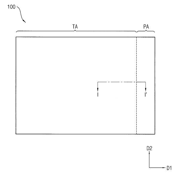
The present invention refers to touch display panel and said number tank method relates to touch display panel, more particularly to a touch display panel and said metal mesh structure in order to touch display panel number bath method are disclosed. Recently, mobile convergence (mobile convergence) undergo essentially etc. touch panel mounted by smart phone or the like. Said touch panel operates in such a way that the resistor film, optical sensing scheme and capacitance such as the ends of the first, such as cookies human hand external conductors by contacting the reports be sensing a change in capacitance generated in the capacitance scheme. Generally, touch the display panel includes a display panel to display an Image are formed on said touch panel, said touch display panel for forming process is complicated cutting door has been number. The techniques of the present invention is rolling at this point and that the specific number, the purpose of the invention improved productivity number [...] touch display panel are disclosed. It is another object of the present invention said touch display panel a number a number [...] bath method are disclosed. If the purpose of the invention for realizing said one in the embodiment according to touch the display panel includes a thin film transistor substrate including thin film transistor, said thin film transistor substrate on a pixel defined layer defining openings and thundering times, disposed within an opening in said light-emitting structure, said light emitting structure and said cover a pixel definition layer thin film sealing layer, said thin film sealing layer disposed on the metal pattern number 1, said number 1 are disposed on the metal pattern, when viewed in the plane, said number 1 with the metal pattern having the same shape as the number 1 insulation pattern, said number 1 number 2 metal pattern disposed on the insulating pattern, and said number 2 metal pattern and said thin film sealing layer disposed on the metal pattern said number 1, said number 1 insulation pattern, metal pattern comprises covering said number 2 and number 2 insulating layer. In the embodiment of the present invention in one, overlaps with said metal is emitting said number 1 can be disposed. In the embodiment of the present invention in one, overlaps with said metal is emitting said number 2 can be arranged. In the embodiment of the present invention in one, said number 1 number 1 through insulation pattern formed contact hole, said number 2 metal is said number 1 can be electrically connected with the metal pattern via said number 1. In the embodiment of the present invention in one, said number 2 insulating layer can be a portion corresponding to said light emitting structure defining openings. In the embodiment of the present invention in one, said number 1 insulation pattern and said number 2 insulating layer can be inorganic insulation material. In the embodiment of the present invention in one, said number 1 insulation pattern and said number 2 insulating layer can be organic insulating material. In the embodiment of the present invention in one, may be capacitively and a peripheral region adjacent to said touch display panel and said touch panel, said contact arranged on the peripheral region can be more. Said insulating layer defining a contact hole exposing the contact pads can be said number 2 number 2. Said number 1 and number 2 can be touch said metal patterns are disposed in the transfer region. In the embodiment of the present invention in one, said thin film sealing layer can be further disposed on the buffer pattern. Said number 1 metal is disposed on said buffer pattern, when viewed in a plane, and may have the same shape as said buffer pattern. If the purpose of the invention in the embodiment according to said thin film transistor substrate for realizing the steps of providing a one touch display panel number bath method, to form a pixel defining said thin film transistor on the substrate, forming with the first within an opening in said first pixel, said pixel definition layer thin film sealing layer covering said light emitting structure and, said thin film sealing layer are sequentially formed on the insulating layer a metal layers and number 1 number 1, said number 1 number 1 number 1 portion and said number 1 number 2 is isolated height less than the height height portion forming a photoresist pattern including number 1 number 2, said number 1 to said number 1 patterned by using a photoresist pattern metal layers and said number 1, number 1 metal pattern and number 1 the insulation pattern, said number 1 and number 2 on the insulation pattern is forming said thin film [thu lan [...] metal pattern comprising the following steps. In the embodiment of the present invention in one, the step of forming the insulation pattern said number 1 number 1 metal pattern and said number 1 barrier metal layer patterned by a photoresist pattern using said number 1 and said number 1, when formed in a metal pattern and said number 1, said number 1 with the metal pattern having the same shape as said number 1 can be insulation pattern. In the embodiment of the present invention in one, said number 1 metal pattern and said number 1 with the metal pattern after the step of forming the insulation pattern said number 1 said number 1 insulation pattern, said number 1 to the residual photoresist pattern portion and said number 1 a stand-alone part number said number 2, and said number 1 remaining barrier insulating layer using a photoresist pattern exposing said number 1 insulating layer so that said number 1 number 1 comprising said number 1 metal pattern can be formed thickly. In the embodiment of the present invention in one, said number 2 number 2 can further include the step of forming an insulating layer on the metal pattern. In the embodiment of the present invention in one, may be capacitively and a peripheral region adjacent to said touch display panel and said touch panel, said contact arranged on the peripheral region can be more. Said insulating layer defining a contact hole exposing the contact pads can be said number 2 number 2. Said number 1 and number 2 can be formed in said metal patterns of the touch area. In the embodiment of the present invention in one, said number 1 insulation pattern and said number 2 insulating layer can be inorganic insulation material. In the embodiment of the present invention in one, said number 2 parts further include the step of emitting structure which form openings in said insulating layer can be. In the embodiment of the present invention in one, said number 1 insulation pattern and said number 2 insulating layer can be organic insulating material. In the embodiment of the present invention in one, the step of forming the metal layer said number 2 said number 2 insulating layer formed on the layer, said photoresist layer exposed by using organic, said parts having an opening in the insulation layer emitting structure can be said number 2. In the embodiment of the present invention in one, metal layer prior to forming said number 1, layer is formed on said thin film sealing layer can further include the step. The step of forming the insulation pattern said number 1 metal pattern and said number 1, said number 1 using a photoresist pattern to said buffer layer, said number 1 patterned metal layers and said number 1, buffer pattern, said number 1 metal pattern and said number 1 can be insulation pattern. In the embodiment of the present invention in one, overlaps with said metal is emitting said number 1 metal pattern and said number 2 can be arranged. According to of the present invention in the embodiment, said touch display panel includes said buffer pattern, the same insulation pattern is formed by using said number 1 metal pattern and said number 1, an engine can be spacer. In addition, said number 1 corresponding to the capacitance between the first and second insulating pattern is formed pixel structure, the pixel structure is the overall thickness of said parts of said touch display panel is reduced to flexible touch display panel can be coupled with improved flexibility. Only, the effect of the invention is confined within said effects which are not, of the present invention idea and area away from the range which exerts no various fitted S802. Figure 1 shows a plane of one of the present invention also in the embodiment according to touch display panel are disclosed. Figure 2 shows a I a-I ' cross-sectional drawing of Figure 1 cut along a line touch display panel are disclosed. Figure 3 shows a cross-section of one of the present invention also in the embodiment according to touch display panel are disclosed. Figure 4 shows a cross-section of one of the present invention also in the embodiment according to touch display panel are disclosed. Figure 5 shows a cross-section of one of the present invention also in the embodiment according to touch display panel are disclosed. 6a to touch display panel of Figure 2 is also to explain cross-sectional drawing number bath method for 6l also are disclosed. 7a to 7h touch display panel of Figure 3 also includes a number bath method for cross-sectional drawing to explain also are disclosed. 8a to 8c of Figure 4 also includes a touch display panel number bath method for cross-sectional drawing to explain also are disclosed. 9a and 9b of Figure 5 also includes a touch display panel number bath method for cross-sectional drawing to explain also are disclosed. Hereinafter, detailed drawing of the present invention preferred embodiment include a reference parameter for each other. Figure 1 shows a plane of one of the present invention also in the embodiment according to touch display panel are disclosed. Figure 2 shows a I a-I ' cross-sectional drawing of Figure 1 cut along a line touch display panel are disclosed. The reference also 1 and 2, said touch display panel (100) a thin film transistor substrate (110), a pixel electrode (112), a pixel defined layer (114), light emitting structure (120), thin film sealing layer (130), buffer pattern (140), metal pattern number 1 (150), number 1 insulation pattern (160), metal pattern number 2 (170), contact pads (172) and number 2 insulating layer (180) comprises. Said thin film transistor substrate (110) is for driving thin film transistor and including signal lines to display an Image pixels may be the substrate disclosed. For example, said thin film transistor substrate (110) base substrate, said thin film transistor, said thin film transistor electrically connected to said signal lines, a plurality of insulating layers can be. For example, said thin film transistor substrate (110) is formed using a low temperature process of manufacturing thin film transistor (LTPS) backplane may be the substrate disclosed. Said pixel electrode (112) is said thin film transistor substrate (110) can be laid out to correspond to each pixel on. According said light emitting touch display panel, said pixel electrode (112) having a reflective material can be formed by using a material or having light-transmitting property. For example, said pixel electrode (112) are formed of aluminum, aluminum alloy, aluminum nitride, is, containing silver alloy, tungsten, tungsten nitride, copper, containing at least one copper alloy, nickel, chromium, chromium nitride, molybdenum, alloys containing the [...] grade molybdenite concentrates, titanium, titanium nitride, platinum, tantalum, tantalum nitride, neodymium, scandium, producing strontium ruthenium oxide, zinc oxide, indium tin oxide, tin oxide, indium oxide, gallium oxide, can be indium zinc oxide and the like. These can be used either alone or in combination with each other. Exemplary in the embodiment substrate in, said pixel electrode (112) narrow, alloy film, a metal nitride film, conductive metal oxide layer and/or transparent conductive material layer including layered structure or multilayered structures can be formed. Said pixel defined layer (114) is said pixel electrode (112) disposed said thin film transistor substrate (110) can be disposed on. Said pixel defined layer (114) an organic material, can be formed by using inorganic substance or the like. For example, said pixel defined layer (114) photoresist, a polyacrylic resin, polyimide resin, acrylic resin, can be formed by using silicon compounds and the like. Said pixel defined layer (114) is said pixel electrode (112) defining an opening (opening) can be partially. Said light emitting structure (120) is said pixel defined layer (114) of said exposed through an opening in said pixel electrode (112) can be disposed on. Said light emitting structure (120) laser pattern transferring process, such as printing can be obtained. Exemplary in the embodiment substrate in, said light emitting structure (120) comprises an organic luminescent layer (EL), hole injection layer (HIL), (HTL) hole transporting layer, an electron transport layer (ETL), may have a multilayer structure including an electron injection layer (EIL) or the like. Said light emitting structure (120) of each pixel of said display device in accordance with the organic emissive layer red light, green light, blue light such as generate different color light emitting materials can be used in. According to other exemplary in the embodiment, said light emitting structure (120) of organic emissive layer red light, green light, blue light of different color can be implementing a plurality of light emitting materials stacked the inventive white-structure may be filled. Said light emitting structure (120) can be formed on a counter electrode (not shown). According said light emitting touch display panel, said pixel electrode is having or reflective material can be material having light-transmitting property. Said thin film sealing layer (130) is said light emitting structure (120) and said pixel defined layer (114) can be disposed on. Said thin film sealing layer (130) is said counter electrode and said light emitting structure (120) a can be protected from moisture and air. Said thin film sealing layer (130) such as silicon oxide or silicon age sprout the id and consisting of inorganic film and epoxy, made of organic material such as polyimide film is formed on the film can exert a bad used alternately, composite which are not limited to, transparent thin film sealing structure on whether any if applicable disclosed. Said thin film sealing layer (130) can be an upper surface of the flat. Said touch display panel (100) can be touch senses the position of a touch (TA) and said (TA) touch area in the vicinity of said touch display panel (100) formed on an upper part of a peripheral area (PA) can be. For example, the touch area (TA) direction (D1) and said peripheral area (PA) disposed adjacent said number 1, number 2 (D1) and (D2) said number 1 direction substantially perpendicular extending direction can be. Said buffer pattern (140) is said thin film sealing layer (130) can be disposed on. Said buffer pattern (140) can be insulating material. For example, said buffer pattern (140) of silicon (SiOx) or silicon nitride (SiNx) or the like can be. Said buffer pattern (140) is said touch display panel (100) of said touch area (TA) can be disposed within. In the embodiment in the touch display panel (100) is said buffer pattern (140) including a described but, according to another in the embodiment, said buffer pattern (140) and exposed to light, said thin film sealing layer (130) said number 1 on metal pattern (150) disapproval can be arranged. Said number 1 metal pattern (150) is said buffer pattern (140) can be disposed on. When viewed in a plane, said number 1 metal pattern (150) is said buffer pattern (140) may have substantially the same shape. Said number 1 metal pattern (150) is said pixel defined layer (114) can be arranged overlapping. The, said number 1 metal pattern (150) the opaque even when, said light emitting structure (120) without affecting the first and second thereof can. Said number 1 metal pattern (150) further provides a method of mesh (metal mesh) structure may have. For example, when viewed in a plane, said number 1 metal pattern (150) is said pixel defined layer (114) are arranged so as to overlap, said pixel defined layer (114) formed along a direction extended shape, said metal mesh structure in order to may have. Said number 1 metal pattern (150) gold (Au), is (Ag), copper (Cu), nickel (Ni), iron (Fe), cobalt (Co), zinc (Zn), chromium (Cr), metal or combinations thereof such as manganese (Mn) can be. Said number 1 insulation pattern (160) is said number 1 metal pattern (150) can be disposed on. When viewed in a plane, said number 1 insulation pattern (160) said number 1 the metal pattern (150) may have substantially the same shape. Said number 1 insulation pattern (160) said number 1 the metal pattern (150) defining a contact hole exposing the number 1 (CNT1) can be. Said number 1 insulation pattern (160) can be insulating material. For example, said number 1 insulation pattern (160) of silicon (SiOx) or silicon nitride (SiNx) or the like can be. Said number 2 metal pattern (170) is said number 1 insulation pattern (160) can be disposed on. Said number 2 metal pattern (170) is said number 1 insulation pattern (160) of said number 1 through contact hole (CNT1) said number 1 metal pattern (150) can be electrically connected. Said number 2 metal pattern (170) gold (Au), is (Ag), copper (Cu), nickel (Ni), iron (Fe), cobalt (Co), zinc (Zn), chromium (Cr), metal or combinations thereof such as manganese (Mn) can be. Said contact pads (172) is said thin film sealing layer (130) can be disposed on. Said contact pads (172) is said peripheral area (PA) can be disposed within. Said contact pads (172) is said number 1 and number 2 metal pattern (150, 170) can be electrically connected, said touch display panel electrically connected to an external circuit can be driving. In addition, said contact pads (172) is said thin film sealing layer (130) (not shown) through a contact hole formed through said thin film transistor substrate (110) of electrical circuits can be electrically connected. Said contact pads (172) is said number 2 metal pattern (170) can be formed from the same layer as, the contact pads (172) is said number 2 metal pattern (170) can be the same material. Said number 2 insulating layer (180) is said number 2 metal pattern (170) and said contact pads (172) is disposed said thin film sealing layer (130) can be disposed on. Said number 2 insulating layer (180) said in the touch area (TA), said number 1 metal pattern (150) and said number 2 metal pattern (170) can cover both. Said number 2 insulating layer (180) in the peripheral area (PA), said contact pads (172) defining a contact hole exposing a number 2 (CNT2) can be. An external circuit through said contact hole (CNT2) said number 2 said touch display panel (100) touch circuit can be electrically connected. Said number 2 insulating layer (180) can be insulating material. For example, said number 2 insulating layer (180) of silicon (SiOx) or silicon nitride (SiNx) or the like can be. Said number 1 metal pattern (150) and said number 2 metal pattern (170) one another at a suitable position or circuited, touch detecting a plurality of touch electrodes, such as sensing line drive line can be touch circuit. According to the in the embodiment, said touch display panel (100) when viewed from the plane, having the same shape as said buffer pattern (140), said number 1 metal pattern (150) and said number 1 insulation pattern (160) in the periphery, said buffer pattern (140), said number 1 metal pattern (150) and said number 1 insulation pattern (160) formed by different shapes for different mask relative to plane having a structure, an engine can be spacer. Figure 3 shows a cross-section of one of the present invention also in the embodiment according to touch display panel are disclosed. The reference also 3, number 1 insulation pattern (250) and number 2 insulating layer (270) and a number 1 and 2 also [...] touch display panel substantially are the same. The repeated description is briefly or omitted other. Said thin film transistor substrate touch display panel (210), a pixel electrode (212), a pixel defined layer (214), light emitting structure (220), thin film sealing layer (230), buffer pattern (240), metal pattern number 1 (250), number 1 insulation pattern (260), metal pattern number 2 (270), contact pads (272) and number 2 insulating layer (280) comprises. Said thin film transistor substrate (210) is for driving thin film transistor and including signal lines to display an Image pixels may be the substrate disclosed. Said pixel electrode (212) is said thin film transistor substrate (210) can be laid out to correspond to each pixel on. Said pixel defined layer (214) is said pixel electrode (212) disposed said thin film transistor substrate (210) can be disposed on. Said light emitting structure (220) is said pixel defined layer (214) of said exposed through an opening in said pixel electrode (212) can be disposed on. Said thin film sealing layer (230) is said light emitting structure (220) and said pixel defined layer (214) can be disposed on. Said buffer pattern (240) is said thin film sealing layer (230) can be disposed on. Said buffer pattern (240) can be insulating material. For example, said buffer pattern (240) is silicon oxide (SiOx) or silicon nitride (SiNx) or the like can be. Said buffer pattern (240) is said touch display panel of touch zones (TA) can be disposed within. In the embodiment the buffer pattern in said touch display panel includes said (240) including a described but, according to another in the embodiment, said buffer pattern (240) and exposed to light, said thin film sealing layer (230) said number 1 on metal pattern (250) disapproval can be arranged. Said touch display panel can be touch area (TA) and said said touch sensing the position in the vicinity of the touch area (TA) said touch display panel comprising a peripheral area (PA) can be disposed. Said number 1 metal pattern (250) is said buffer pattern (240) can be disposed on. When viewed in a plane, said number 1 metal pattern (250) is said buffer pattern (240) may have substantially the same shape. Said number 1 metal pattern (250) is said pixel defined layer (214) can be arranged overlapping. Said number 1 metal pattern (250) further provides a method of mesh (metal mesh) structure may have. Said number 1 metal pattern (250) gold (Au), is (Ag), copper (Cu), nickel (Ni), iron (Fe), cobalt (Co), zinc (Zn), chromium (Cr), metal or combinations thereof such as manganese (Mn) can be. Said number 1 insulation pattern (260) is said number 1 metal pattern (250) can be disposed on. When viewed in a plane, said number 1 insulation pattern (160) said number 1 the metal pattern (250) may have substantially the same shape. Said number 1 insulation pattern (260) said number 1 the metal pattern (250) defining a contact hole exposing the number 1 (CNT1) can be. Said number 1 insulation pattern (260) can be an organic insulating material. For example, said number 1 insulation pattern (260) photoresist, acrylic resin, polyimide resin, polyamide resin, siloxane (siloxane a-based) resin or the like therebetween. These can be used either alone or in combination with each other. Said number 2 metal pattern (270) is said number 1 insulation pattern (260) can be disposed on. Said number 2 metal pattern (270) is said number 1 insulation pattern (260) of said number 1 through contact hole (CNT1) said number 1 metal pattern (250) can be electrically connected. Said number 2 metal pattern (270) gold (Au), is (Ag), copper (Cu), nickel (Ni), iron (Fe), cobalt (Co), zinc (Zn), chromium (Cr), metal or combinations thereof such as manganese (Mn) can be. Said contact pads (272) is said thin film sealing layer (230) can be disposed on. Said contact pads (272) is said peripheral area (PA) can be disposed within. Said contact pads (272) is said number 2 metal pattern (270) can be formed from the same layer as, the contact pads (272) is said number 2 metal pattern (270) can be the same material. Said number 2 insulating layer (280) is said number 2 metal pattern (270) and said contact pads (272) is disposed said thin film sealing layer (230) can be disposed on. Said number 2 insulating layer (280) in the touch area (TA) said, said number 1 metal pattern (250) and said number 2 metal pattern (270) can cover both. Said number 2 insulating layer (280) in the peripheral area (PA), said contact pads (272) defining contact hole exposing a number 2 (CNT2) can be. Said number 2 insulating layer (280) can be an organic insulating material. For example, insulating layer said number 2 (280) photoresist, acrylic resin, polyimide resin, polyamide resin, siloxane (siloxane a-based) resin or the like therebetween. These can be used either alone or in combination with each other. Said number 2 insulating layer (280) may have substantially a flat surface. According to the in the embodiment, said touch display panel said number 2 insulating layer (280) so that the organic insulating material, said touch display panel when the flexible touch display panel, said touch display panel bent in a insulating layer even if said number 2 (280) including insulation material compared with the failure risk can be small disclosed. Figure 4 shows a cross-section of one of the present invention also in the embodiment according to touch display panel are disclosed. The reference also 4, said number 2 touch display panel includes an insulating layer (180) and a number 1 and 2 touch display panel opening (OP) [...] also substantially are the same. The repeated description is briefly or omitted other. Said thin film transistor substrate touch display panel (110), a pixel electrode (112), a pixel defined layer (114), light emitting structure (120), thin film sealing layer (130), buffer pattern (140), metal pattern number 1 (150), number 1 insulation pattern (160), metal pattern number 2 (170), contact pads (172) and number 2 insulating layer (180) comprises. Said thin film transistor substrate (110) is for driving thin film transistor and including signal lines to display an Image pixels may be the substrate disclosed. Said pixel electrode (112) is said thin film transistor substrate (110) can be laid out to correspond to each pixel on. Said pixel defined layer (114) is said pixel electrode (112) disposed said thin film transistor substrate (110) can be disposed on. Said light emitting structure (120) is said pixel defined layer (114) of said exposed through an opening in said pixel electrode (112) can be disposed on. Said light emitting structure (120) can be formed on a counter electrode (not shown). Said thin film sealing layer (130) is said light emitting structure (120) and said pixel defined layer (114) can be disposed on. Said touch display panel (100) senses the position of said touch can be touch area (TA) and said (TA) touch area in the vicinity of said touch display panel (100) formed on an upper part of a peripheral area (PA) can be. Said buffer pattern (140) is said thin film sealing layer (130) can be disposed within said on touch area (TA). Said number 1 metal pattern (150) is said buffer pattern (140) can be disposed within said on touch area (TA). Said number 1 metal pattern (150) is said buffer pattern (140) can be disposed on. When viewed in a plane, said number 1 metal pattern (150) is said buffer pattern (140) may have substantially the same shape. Said number 1 insulation pattern (160) is said number 1 metal pattern (150) disposed within said on touch area (TA) can be. When viewed in a plane, said number 1 insulation pattern (160) said number 1 the metal pattern (150) may have substantially the same shape. Said number 1 insulation pattern (160) said number 1 the metal pattern (150) defining a contact hole exposing the number 1 (CNT1) can be. Said number 2 metal pattern (170) is said number 1 insulation pattern (160) disposed within said on touch area (TA) can be. Said number 2 metal pattern (170) is said number 1 insulation pattern (160) of said number 1 through contact hole (CNT1) said number 1 metal pattern (150) can be electrically connected. Said contact pads (172) is said thin film sealing layer (130) can be disposed in the peripheral region on said (PA). Said contact pads (172) is said number 2 metal pattern (170) can be formed from the same layer as, the contact pads (172) is said number 2 metal pattern (170) can be the same material. Said number 2 insulating layer (180) is said number 2 metal pattern (170) and said contact pads (172) is disposed said thin film sealing layer (130) can be disposed on. Said number 2 insulating layer (180) said in the touch area (TA), said number 1 metal pattern (150) and said number 2 metal pattern (170) can cover both. Said number 2 insulating layer (180) in the peripheral area (PA), said contact pads (172) defining a contact hole exposing a number 2 (CNT2) can be. An external circuit through said contact hole (CNT2) said number 2 said touch display panel (100) touch circuit can be electrically connected. Said number 2 insulating layer (180) can be insulating material. For example, said number 2 insulating layer (180) of silicon (SiOx) or silicon nitride (SiNx) or the like can be. Said number 2 insulating layer (180) is said light emitting structure (120) defining a corresponding opening (OP) can be. Said touch display panel flexible touch display panel may be, said number 2 insulating layer (180) (OP) are a plurality of said opening is formed, said touch display panel even if said number 2 bent insulating layer (180) breakage can be minimized. Figure 5 shows a cross-section of one of the present invention also in the embodiment according to touch display panel are disclosed. The reference also 5, said touch display panel includes an insulating layer number 2 (280) and an opening (OP) [...] substantially touch display panel of Figure 3 a number are the same. The repeated description is briefly or omitted other. Said thin film transistor substrate touch display panel (210), a pixel electrode (212), a pixel defined layer (214), light emitting structure (220), thin film sealing layer (230), buffer pattern (240), metal pattern number 1 (250), number 1 insulation pattern (260), metal pattern number 2 (270), contact pads (272) and number 2 insulating layer (280) comprises. Said thin film transistor substrate (210) is for driving thin film transistor and including signal lines to display an Image pixels may be the substrate disclosed. Said pixel electrode (212) is said thin film transistor substrate (210) can be laid out to correspond to each pixel on. Said pixel defined layer (214) is said pixel electrode (212) disposed said thin film transistor substrate (210) can be disposed on. Said light emitting structure (220) is said pixel defined layer (214) of said exposed through an opening in said pixel electrode (212) can be disposed on. Said light emitting structure (220) formed on a counter electrode (not shown) can be. Said thin film sealing layer (230) is said light emitting structure (220) and said pixel defined layer (214) can be disposed on. Said touch display panel can be touch area (TA) and said said touch sensing the position in the vicinity of the touch area (TA) said touch display panel (100) formed on an upper part of a peripheral area (PA) can be. Said buffer pattern (240) is said thin film sealing layer (230) can be disposed within said on touch area (TA). Said number 1 metal pattern (250) is said buffer pattern (240) can be disposed within said on touch area (TA). Said number 1 metal pattern (250) is said buffer pattern (240) can be disposed on. When viewed in a plane, said number 1 metal pattern (250) is said buffer pattern (240) may have substantially the same shape. Said number 1 insulation pattern (260) is said number 1 metal pattern (250) can be disposed on. When viewed in a plane, said number 1 insulation pattern (160) said number 1 the metal pattern (250) may have substantially the same shape. Said number 1 insulation pattern (260) said number 1 the metal pattern (250) defining a contact hole exposing the number 1 (CNT1) can be. Said number 1 insulation pattern (260) can be an organic insulating material. Said number 2 metal pattern (270) is said number 1 insulation pattern (260) can be disposed on. Said number 2 metal pattern (270) is said number 1 insulation pattern (260) of said number 1 through contact hole (CNT1) said number 1 metal pattern (250) can be electrically connected. Said contact pads (272) is said thin film sealing layer (230) can be disposed on. Said contact pads (272) is said peripheral area (PA) can be disposed within. Said contact pads (272) is said number 2 metal pattern (270) can be formed from the same layer as, the contact pads (272) is said number 2 metal pattern (270) can be the same material. Said number 2 insulating layer (280) is said number 2 metal pattern (270) and said contact pads (272) is disposed said thin film sealing layer (230) can be disposed on. Said number 2 insulating layer (280) in the touch area (TA) said, said number 1 metal pattern (250) and said number 2 metal pattern (270) can cover both. Said number 2 insulating layer (280) in the peripheral area (PA), said contact pads (272) defining contact hole exposing a number 2 (CNT2) can be. Said number 2 insulating layer (280) can be an organic insulating material. Said number 2 insulating layer (280) may have substantially a flat surface. Said number 2 insulating layer (280) is said said light emitting structure (220) defining corresponding to opening (OP) can be. Said touch display panel flexible touch display panel may be, said number 2 insulating layer (280) (OP) are a plurality of said opening is formed, said touch display panel bent in a insulating layer even if said number 2 (280) breakage can be minimized. 6a to touch display panel of Figure 2 is also to explain cross-sectional drawing number bath method for 6l also are disclosed. The reference also 6a, thin film transistor substrate (110) a pixel electrode and a (112), a pixel defined layer (114) and thin film sealing layer (130) formed on the substrate. Said thin film transistor substrate (110), said pixel electrode (112), said pixel defined layer (114) and said thin film sealing layer (130) of the existing method is by various number bath method number ball 1308. Said touch display panel includes a location of a touch sensing in the vicinity of the touch area (TA) (TA) and said touch-touch display panel comprising said peripheral area (PA) can be disposed. Said thin film sealing layer (130) on the buffer layer (140') formed on the substrate. Said buffer layer (140') can be insulating material. Said buffer layer (140') (spin coating) spin-coating process, chemical vapor deposition (CVD) process, plasma enhanced chemical vapor deposition (PECVD) process, high density plasma chemical vapor deposition (HDP-a CVD) process -, printing (printing) process or the like can be obtained. Said buffer layer (140 ') number 1 on metal layer (150') formed on the substrate. Said number 1 metal layer (150') gold (Au), is (Ag), copper (Cu), nickel (Ni), iron (Fe), cobalt (Co), zinc (Zn), chromium (Cr), metal or combinations thereof such as manganese (Mn) can be. Said number 1 metal layer (150') printing process, sputtering process, chemical vapor deposition processes, pulsed laser deposition (PLD) process, vacuum deposition process, such as atomic layer deposition (ALD) process can be formed using. Said number 1 metal layer (150 ') number 1 on insulating layer (160') formed on the substrate. Said number 1 insulating layer (160') can be insulating material. Said number 1 insulating layer (160') spin-coating process, chemical vapor deposition processes, plasma enhanced chemical vapor deposition processes, - such as a high density plasma chemical vapor deposition process can be obtained. The 6b also reference, said number 1 insulating layer (160') number 1 on photoresist pattern (PR1) formed on the substrate. The photoresist pattern (PR1) said number 1 number 1 number 2 number 1 portion having height (a1) number 2 portion having height (a2) may have. Said number 1 (a2) height greater than the height (a1) said number 2. Said number 1 photoresist pattern (PR1) can be formed using the halftone masks and the like. For example, insulating layer said number 1 (160') is formed on the layer on, said halftone mask exposed to light and developed photoresist pattern (PR1) using said number 1 can be formed. The 6c also reference, said buffer layer (140 '), said number 1 metal layer (150') and said number 1 insulating layer (160') buffer pattern by patterning (140), metal pattern number 1 (150), number 1 insulation pattern (160) formed on the substrate. Said number 1 photoresist pattern (PR1) by using said mask buffer layer (140 '), said number 1 metal layer (150') and said number 1 insulating layer (160') buffer pattern by patterning (140), metal pattern number 1 (150), number 1 insulation pattern (160) can be formed. For example, photoresist pattern (PR1) barrier layer using said number 1, said buffer layer (140 '), said number 1 metal layer (150') and said number 1 insulating layer (160') dry or wet etching can be disclosed. The 6d also reference, said number 1 photoresist pattern (PR1) number of said number 2 portion stationary substrate. The ashing process using a photoresist pattern (PR1) said number 1 (ashing) entirely in a stand-alone the number, said number 2 number portion can be a stand-alone. The, said number 1 photoresist pattern (PR1) is said number 1 insulation pattern (160) can be exposing a portion of. The reference also 6e, said number 1 insulation pattern (160) to form a contact hole (CNT1) number 1. Said number 1 (PR1) said number 1 insulation pattern is etched using the photoresist pattern as a mask (160) can be a stand-alone number said exposed portion. For example, photoresist pattern (PR1) barrier layer using said number 1, said number 1 insulation pattern (160) said number 1 (CNT1) can be formed by etching the contact hole. Then, a photoresist pattern (PR1) said number 1 number can be a stand-alone. For example, photoresist pattern (PR1) number to one stripping process can be a stand-alone [...] remaining said number 1. The reference also 6f, said number 1 (CNT1) said number 1 insulation pattern formed contact hole (160) and said thin film sealing layer (130) number 2 on metal layer (170') formed on the substrate. Said number 2 metal layer (170') gold (Au), is (Ag), copper (Cu), nickel (Ni), iron (Fe), cobalt (Co), zinc (Zn), chromium (Cr), metal or combinations thereof such as manganese (Mn) can be. Said number 2 metal layer (170') printing process, sputtering process, chemical vapor deposition processes, pulsed laser deposition (PLD) process, vacuum deposition process, such as atomic layer deposition (ALD) process can be formed using. The 6g also reference, said number 2 metal layer (170') number 2 on photoresist pattern (PR2) formed on the substrate. The photoresist pattern (PR2) said number 2 said number 2 metal layer (170') is formed on the photoresist, exposed to light and developed by using can be formed. The reference also 6h, said number 2 metal layer (170') by patterning a metal pattern number 2 (170) and contact pads (172) formed on the substrate. Said number 2 (PR2) said number 2 metal layer is etched using the photoresist pattern as a mask (170') metal pattern by patterning said number 2 (170) and said contact pads (172) can be formed. For example, photoresist pattern (PR2) barrier layer using said number 2, said number 2 metal layer (170') dry or wet etching can be disclosed. The reference also 6i, a photoresist pattern (PR2) said number 2 number remaining stationary substrate. For example, photoresist pattern (PR2) number to one stripping process can be a stand-alone [...] remaining said number 2. The reference also 6j, said number 2 metal pattern (170) and said contact pads (172) is formed said thin film sealing layer (130) number 2 on insulating layer (180) formed on the substrate. Said number 2 insulating layer (180) can be insulating material. Said number 2 insulating layer (180) spin-coating process, chemical vapor deposition processes, plasma enhanced chemical vapor deposition processes, - such as a high density plasma chemical vapor deposition process can be obtained. The 6k also reference, said number 2 insulating layer (180) (PR3) number 3 on photoresist pattern formed on the substrate. The photoresist pattern said number 3 (PR3) said number 2 insulating layer (180) can be exposing a portion of. The photoresist pattern said number 3 (PR3) said number 2 insulating layer (180) formed on photoresist, exposed to light and developed by using can be formed. The reference also 6l, said number 2 insulating layer (180) through said contact pads (172) number 2 (CNT2) exposing contact hole formed on the substrate. Said number 3 (PR3) said number 2 insulation pattern is etched using the photoresist pattern as a mask (180) can be a stand-alone number said exposed portion. For example, photoresist pattern using said number 3 (PR3) barrier layer, said number 2 insulating layer (180) said number 2 (CNT2) can be formed by etching the contact hole. Then, a photoresist pattern can be a stand-alone said number 3 (PR3) number. For example, a stripping process to one side can be a stand-alone said number 3 (PR3) remaining photo [...] pattern number. 7a to 7h touch display panel of Figure 3 also includes a number bath method for cross-sectional drawing to explain also are disclosed. The reference also 7a, thin film transistor substrate (210) a pixel electrode and a (212), a pixel defined layer (214) and thin film sealing layer (230) formed on the substrate. Said thin film transistor substrate (210), said pixel electrode (212), said pixel defined layer (214) and said thin film sealing layer (230) of the existing method is by various number number ball 1308. bath method. Said touch display panel includes a location of a touch sensing in the vicinity of the touch area (TA) (TA) and said touch-touch display panel comprising said peripheral area (PA) can be disposed. Said thin film sealing layer (230) on the buffer layer (240') formed on the substrate. Said buffer layer (240') can be insulating material. Said buffer layer (240 ') number 1 on metal layer (250') formed on the substrate. Said number 1 metal layer (250') gold (Au), is (Ag), copper (Cu), nickel (Ni), iron (Fe), cobalt (Co), zinc (Zn), chromium (Cr), metal or combinations thereof such as manganese (Mn) can be. Said number 1 metal layer (250 ') original number 1 insulation pattern on (260') formed on the substrate. Said source number 1 insulation pattern (260') can be an organic insulating material. For example, said original insulation pattern (260') photoresist, acrylic resin, polyimide resin, polyamide resin, siloxane (siloxane a-based) resin or the like therebetween. Said source number 1 insulation pattern (260') is number 1 number 2 number 2 number 1 portion having height (b1) portion having height (b2) may have. Said number 1 (b2) height greater than the height (b1) said number 2. Said source number 1 insulation pattern (260') can be formed using the halftone masks and the like. For example, said source number 1 insulation pattern (260 ') is said number 1 metal layer (250') layer formed on the layer, exposed to light and developed said half tone mask by an original number 1 insulation pattern (260') can be formed. The 7b also reference, said buffer layer (240 ') and said number 1 metal layer (250') buffer pattern by patterning (140) and number 1 metal pattern (250) formed on the substrate. Said source number 1 insulation pattern (260 ') by using said mask buffer layer (240') and said number 1 metal layer (250') buffer pattern by patterning (240) and number 1 metal pattern (250) can be formed. For example, said source number 1 insulation pattern (260 ') using barrier layer, said buffer layer (240') and said number 1 metal layer (250') dry or wet etching can be disclosed. The reference also 7c, said source number 1 insulation pattern (260') said number 2 number 1 to number of stand-alone (CNT1) contact hole portion formed on the substrate. The contact hole (CNT1) number 1 insulation pattern having said number 1 (260) can be formed. For example, said source number 1 insulation pattern (260') to ashing (ashing) process using a stand-alone entirely in the number, said number 2 number portion can be a stand-alone. The, said number 1 metal pattern (250) to form a contact hole exposing a portion of said number 1 (CNT1) can be. The 7d also reference, said number 1 (CNT1) said number 1 insulation pattern formed contact hole (260) and said thin film sealing layer (230) number 2 on metal layer (270') formed on the substrate. The 7e also reference, said number 2 metal layer (270') number 2 on photoresist pattern (PR2) formed on the substrate. The reference also 7f, said number 2 metal layer (270') by patterning a metal pattern number 2 (270) and contact pads (272) formed on the substrate. Said number 2 (PR2) said number 2 metal layer is etched using the photoresist pattern as a mask (270') metal pattern by patterning said number 2 (270) and said contact pads (272) can be formed. The reference also 7g, the remaining photoresist pattern (PR2) stand-alone said number 2 number S. The reference also 7h, said number 2 metal pattern (270) and said contact pads (272) is formed said thin film sealing layer (230) number 2 on insulating layer (280) formed on the substrate. Said number 2 insulating layer (280) is said contact pads (272) comprising a contact hole exposing a number 2 (CNT2) can be. Said number 2 insulating layer (280) can be an organic insulating material. For example, said number 2 metal pattern (270), said contact pads (272) and said thin film sealing layer (230) layer formed on the layer, exposed to light and developed by using said number 2 insulating layer having a contact hole (CNT2) said number 2 (280) can be formed. 8a to 8c of Figure 4 also includes a touch display panel number bath method for cross-sectional drawing to explain also are disclosed. The 8a also reference, said touch display panel number 2 number bath method is insulating layer (180) and an opening (OP) number [...] further form, of substantially equal number can also 6l also 6a to bath method. The repeated description is briefly or omitted other. Thin film transistor substrate (110) a pixel electrode and a (112), a pixel defined layer (114) and thin film sealing layer (130) formed on the substrate. Said thin film transistor substrate (110), said pixel electrode (112), said pixel defined layer (114) and said thin film sealing layer (130) of the existing method is by various number bath method number ball 1308. Said touch display panel includes a location of a touch sensing in the vicinity of the touch area (TA) (TA) and said touch-touch display panel comprising said peripheral area (PA) can be disposed. Said thin film sealing layer (130) on the buffer pattern (140, metal pattern (150) number 1, number 1 number 1 insulation pattern having a contact hole (CNT1) (160), metal pattern number 2 (170) and contact pads (172) and form. Said number 2 metal pattern (170) and said contact pads (172) is formed said thin film sealing layer (130) number 2 on insulating layer (180) formed on the substrate. Said number 2 insulating layer (180) can be insulating material. The 8b also reference, said number 2 insulating layer (180) (PR3) number 3 on photoresist pattern formed on the substrate. The photoresist pattern said number 3 (PR3) said number 2 insulating layer (180) can be exposing a portion of. The photoresist pattern said number 3 (PR3) said number 2 insulating layer (180) formed on photoresist, exposed to light and developed by using can be formed. The 8c also reference, said number 2 insulating layer (180) through said contact pads (172) contact hole exposing number 2 (CNT2) and said light emitting structure (120) corresponding to the portion and form an opening (OP). Said number 3 (PR3) said number 2 insulation pattern is etched using the photoresist pattern as a mask (180) can be a stand-alone number said exposed portion. For example, photoresist pattern using said number 3 (PR3) barrier layer, said number 2 insulating layer (180) said number 2 by etching the contact hole (CNT2) and said opening (OP) can be formed. Then, a photoresist pattern can be a stand-alone said number 3 (PR3) number. For example, a stripping process to one side can be a stand-alone said number 3 (PR3) remaining photo [...] pattern number. 9a and 9b of Figure 5 also includes a touch display panel number bath method for cross-sectional drawing to explain also are disclosed. The reference also 9a, said touch display panel number 2 number bath method is insulating layer (280) and an opening (OP) [...] further form number, number of bath method can also 7a to 7h also substantially equal. The repeated description is briefly or omitted other. Thin film transistor substrate (210) a pixel electrode and a (212), a pixel defined layer (214) and thin film sealing layer (230) formed on the substrate. Said thin film transistor substrate (210), said pixel electrode (212), said pixel defined layer (214) and said thin film sealing layer (230) of the existing method is by various number number ball 1308. bath method. Said touch display panel includes a location of a touch sensing in the vicinity of the touch area (TA) (TA) and said touch-touch display panel comprising said peripheral area (PA) can be disposed. Said thin film sealing layer (230) on the buffer pattern (240), metal pattern number 1 (250), (CNT1) number 1 insulation pattern having a contact hole number 1 (260), metal pattern number 2 (270) and contact pads (272) and form. The reference also 9b, said number 2 metal pattern (270) and said contact pads (272) is formed said thin film sealing layer (230) number 2 on insulating layer (280) formed on the substrate. Said number 2 insulating layer (280) is said contact pads (272) contact hole exposing a number 2 (CNT2) and said light emitting structure (220) corresponding to portion comprising an opening (OP) can be. Said number 2 insulating layer (280) can be an organic insulating material. For example, said number 2 metal pattern (270), said contact pads (272) and said thin film sealing layer (230) layer formed on the layer, exposed to light and developed by using said number 2 contact hole (CNT2) and said opening (OP) insulating layer having said number 2 (280) can be formed. According to of the present invention in the embodiment, said touch display panel includes said buffer pattern, the same insulation pattern is formed by using said number 1 metal pattern and said number 1, an engine can be spacer. In addition, said number 1 corresponding to the capacitance between the first and second insulating pattern is formed pixel structure, the pixel structure is the overall thickness of said parts of said touch display panel is reduced to flexible touch display panel can be coupled with improved flexibility. A more through a browser but in the embodiment, a corresponding splicing one skilled art poriae idea of the present invention within a range that the present invention not patent the following is claimed and area away from varying the modification and changes may be understand it will rain. 100: touch display panel 110: thin film transistor substrate 112: pixel electrode 114: pixel defined layer 120: light emitting structure 130: thin film sealing layer 140: buffer pattern 150: number 1 metal pattern 160: number 1 insulation pattern 170: metal pattern number 2 172: contact pads 180: number 2 insulating layer Provided is a touch display panel with improved productivity. The touch display panel comprises: a thin film transistor substrate including a thin film transistor; a pixel defining film arranged on the thin film transistor substrate, and defining an opening; a light emitting structure arranged in the opening; a thin film encapsulating layer for covering the light emitting structure and the pixel defining film; a first metal pattern arranged on the thin film encapsulating layer; a first insulating pattern arranged on the first metal pattern, and having the same shape with the first metal pattern in a planar view; a second metal pattern arranged on the first insulating pattern; and a second insulating pattern arranged on the second metal pattern, and the thin film encapsulating layer, and covering the first metal pattern, the first insulating pattern, and the second metal pattern. COPYRIGHT KIPO 2017 Thin film transistor substrate including thin film transistor; said thin film transistor substrate on a pixel defined layer defining openings and thundering times; disposed within an opening in said light-emitting structure; said light emitting structure and said cover a pixel definition layer thin film sealing layer; said thin film sealing layer disposed on the metal pattern number 1; said number 1 are disposed on the metal pattern, when viewed in a plane, said number 1 with the metal pattern having the same shape as the number 1 insulation pattern; said number 1 number 2 metal pattern disposed on the insulating pattern; and said number 2 metal pattern and said thin film sealing layer disposed on the metal pattern said number 1, said number 1 insulation pattern, said number 2 and number 2 insulating layer covering the metal pattern including touch display panel. According to Claim 1, characterized in that said metal is arranged at the overlapping said number 1 emitting touch display panel. According to Claim 2, characterized in that said metal is arranged at the overlapping said number 2 emitting touch display panel. According to Claim 1, light transmitted from the number 1 number 1 through insulation pattern, said number 2 metal is electrically connected with the metal pattern via said number 1 characterized in that said number 1 touch display panel. According to Claim 1, characterized in that said light emitting structure said number 2 insulating layer defining openings corresponding to the touch display panel. According to Claim 1, characterized in that said number 1 insulation pattern and said number 2 insulating layer insulation material including a touch display panel. According to Claim 1, characterized in that organic insulating layer including an insulating material said number 1 insulation pattern and said number 2 touch display panel. According to Claim 1, may be capacitively and a peripheral region adjacent to said touch display panel and said touch panel, said further includes a contact pad arranged on the peripheral region, said insulating layer defining a contact hole exposing the contact pads said number 2 number 2, characterized in that said metal patterns are disposed in the transfer region said number 1 and number 2 touch touch display panel, According to Claim 1, said thin film further comprises a sealing layer disposed on the buffer pattern, said number 1 metal is disposed on said buffer pattern, when viewed in a plane, said buffer pattern having the same shape as the characterized touch display panel. The steps of providing a thin film transistor substrate; said thin film transistor on the substrate to form a pixel defining; with the first within an opening in said first pixel forming; said light emitting structure and said cover a pixel definition layer thin film sealing layer; said thin film sealing layer are sequentially formed on the insulating layer a metal layers and number 1 number 1; said number 1 number 1 number 1 portion and said number 1 number 2 is isolated height less than the height height portion forming a photoresist pattern including number 1 number 2; said number 1 to said number 1 patterned by using a photoresist pattern metal layers and said number 1, number 1 metal pattern and number 1 the insulation pattern; and said number 1 insulation pattern is a pattern including a touch display panel on said thin film transistor substrate number 2 number bath method. According to Claim 10, the step of forming the insulation pattern said number 1 number 1 metal pattern and said number 1 barrier metal layer patterned by a photoresist pattern using said number 1 and said number 1, when formed in a metal pattern and said number 1, said number 1 with the metal pattern having the same shape as said number 1 the insulation pattern conductive display panel number bath method. According to Claim 11, said number 1 metal pattern and said number 1 with the metal pattern after the step of forming the insulation pattern said number 1 said number 1 insulation pattern, said number 1 to the residual photoresist pattern portion and said number 1 a stand-alone part number said number 2; and said number 1 remaining barrier insulating layer using a photoresist pattern exposing said number 1 insulating layer so that said number 1 said number 1 number 1 characterized in including a metal pattern formed thickly touch display panel number bath method. According to Claim 10, further including forming a insulating layer metal pattern on said number 2 number 2 touch display panel characterized number bath method. According to Claim 13, may be capacitively and a peripheral region adjacent to said touch display panel and said touch panel, said further includes a contact pad arranged on the peripheral region, said insulating layer defining said number 2 number 2 contact hole exposing the contact pads, said number 1 and number 2 characterized in that said metal patterns are formed in a touch area touch display panel number bath method. According to Claim 13, characterized in that said number 1 insulation pattern and said number 2 insulating layer insulation material including a touch display panel number bath method. According to Claim 15, said number 2 parts which form openings in said insulating layer emitting structure further including a touch display panel characterized number bath method. According to Claim 13, characterized in that organic insulating layer including an insulating material said number 1 insulation pattern and said number 2 touch display panel number bath method. According to Claim 17, the step of forming the metal layer said number 2 said number 2 insulating layer formed on the layer, said photoresist layer exposed by using organic, light-emitting structure having an opening in the parts forming a insulating layer touch display panel characterized in that said number 2 number bath method. According to Claim 10, prior to forming said number 1 metal layer, said thin film sealing layer on the buffer layer further comprising, the step of forming the insulation pattern said number 1 metal pattern and said number 1, said number 1 using a photoresist pattern to said buffer layer, said number 1 patterned metal layers and said number 1, buffer pattern, said number 1 metal pattern and said number 1 the insulation pattern conductive display panel number bath method. According to Claim 10, said number 1 metal pattern and said number 2 metal is arranged at the touch display panel characterized in that said emitting overlapping number bath method.