SUBSTRATE FOR CAMERA MODULE AND CAMERA MODULE HAVING SAME
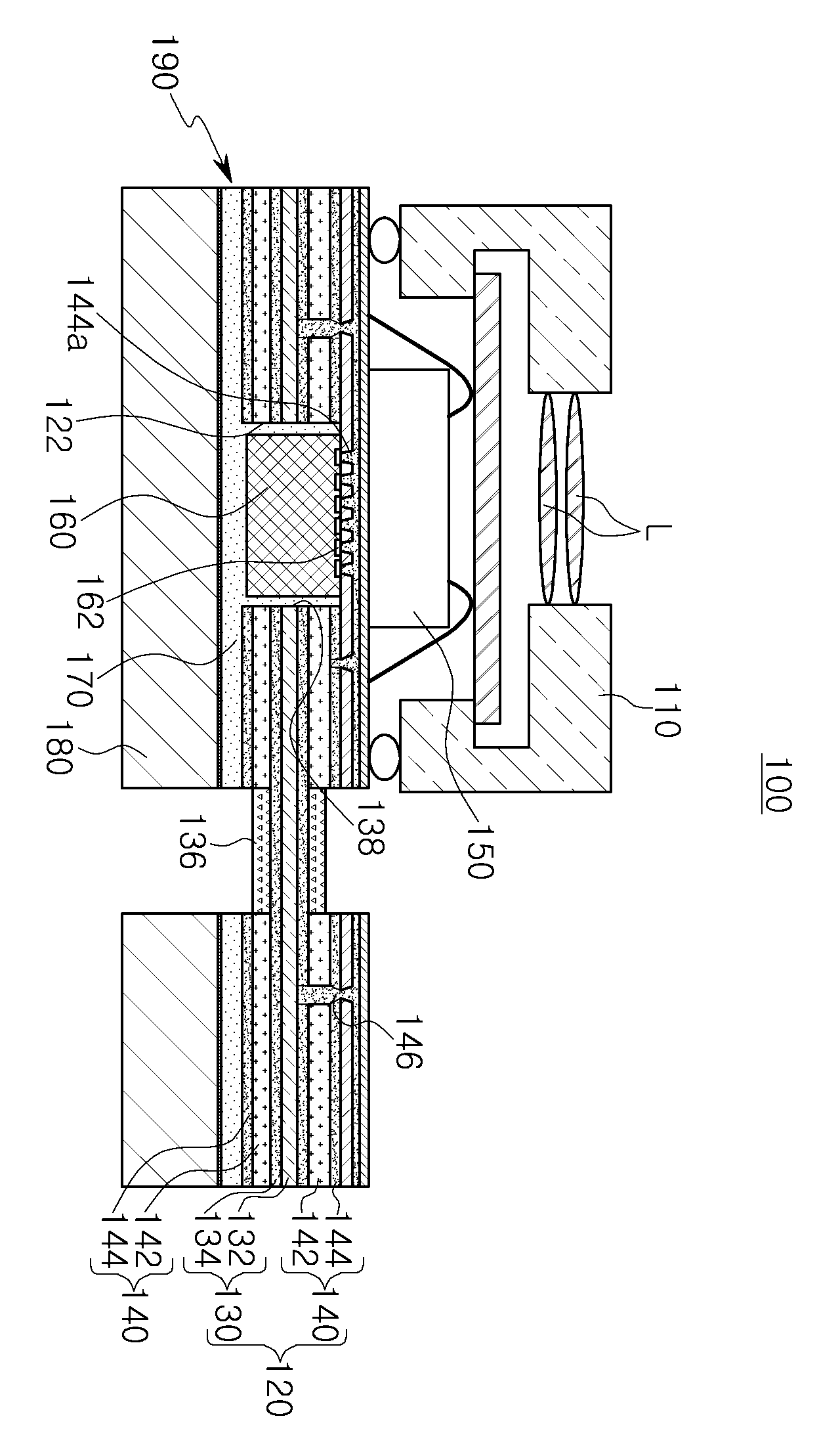
The present invention refers to a camera module substrate for a camera module having the same are disclosed. Recent high-speed photographing (supper slow motion, anti-a distortion shutter) enables the implementation of a high-speed camera module for mobile etc. desired. In this case, extremely high photographing of a vehicle to transmit the necessary memory and controls the sensor Image for Image data processing, memory Image sensor substrate are disposed side door number when camera module increases as the magnitude of flow tides. The, speed without increasing size consistent development of a camera module in a database are disclosed. Very high speed consistent plasma ball number encoded to a camera module for a camera module. In the embodiment according to one of the present invention substrate for a camera module substrate is number 1, number 1 of Image sensor and said number 1 board installed which are embedded in a memory chip, said number 1 the substrate is disposed at the center flexible portion, said flexible portion formed of a wire produce a rigid board, at least a portion of said memory chip can be disposed in a hole formed on said flexible substrate moving. Effect speed consistent flow tides. Figure 1 shows a schematic configuration for a camera module of the present invention number 1 in the embodiment according to the antenna also representing a camera module are disclosed. Figure 2 shows a schematic configuration for a camera module of the present invention number 2 in the embodiment according to the antenna also representing a camera module are disclosed. Figure 3 shows a schematic configuration for a camera module of the present invention number 3 in the embodiment according to the antenna also representing a camera module are disclosed. Figure 4 shows a schematic configuration for a camera module of the present invention number 4 in the embodiment according to the antenna also representing a camera module are disclosed. Figure 5 shows a schematic configuration for a camera module of the present invention number 5 in the embodiment according to the antenna also representing a camera module are disclosed. Hereinafter, a preferred embodiment of the present invention with reference to the attached drawing shapes described substrate. However, various other forms of the present invention embodiment can be shape, embodiment of the present invention hereinafter described form and not the limited range. In addition, the present invention in the field of the present invention embodiment form are advantageously easier to average knowledge with which to more completely account for the ball number are disclosed. Drawing description more specifically for and apparatus or the like in the shape and size of the elements can be. Figure 1 shows a schematic configuration for a camera module of the present invention number 1 in the embodiment according to the antenna also representing a camera module are disclosed. The reference also 1, of the present invention number 1 in the embodiment according to camera module (100) is as an example, lens barrel (110), number 1 substrate (120), Image sensor (150), memory chip (160), resin layer (170) and compressed (180) can be comprising. Lens barrel (110) is installed at least one lens (L), number 1 substrate (120) bonded to the upper surface of force is removed. As an example, lens barrel (110) is made of a shaped, with the inner and/or outer surface can be formed to have at least one step. On the other hand, in the embodiment in a lens barrel (110) when as an example shown in the drawing to 3 of member is fitted for example without intending to be limited, not limited. I.e., lens barrel (110) which is mounted on the number of lenses and lens barrel (110) the shape of the deformable various will. Number 1 substrate (120) is lens barrel (110) cover, Image sensor (150) group is barrel (110) to the lens (L) lower number 1 are arranged in a substrate (120) to force is removed. On the other hand, number 1 substrate (120) is disposed at the center flexible part (130) on, flexible substrate portion (130) of, formed under the rigid board unit (140) can be with. Flexible substrate portion (130) is flexibly bent insulating (132) and, insulating film (132) of the bottom portion of the top of the foil (134) can be with. Further, separated from the flexible substrate portion (130) is provided with a protective layer (136) can be formed. And, flexible substrate portion (130) of the installation hole is (138) is formed, memory chip (160) the installation hole (138) can be disposed. Rigid board unit (140) is ductile substrate part (130) formed part of. Rigid board unit (140) is an insulating layer (142) and pattern layer (144) can be with. And, insulating layer (142) and pattern layer (144) can be formed an electrostrictive. On the other hand, number 1 substrate (120) of memory chip (160) is an ST mounting groove (122) formed therein. Mounting groove (122) flexible substrate part (130) of a lower rigid board unit (140) from flexible part (130) through the flexible part (130) is disposed on top of the rigid board portion (140) formed up. I.e., mounting groove (122) flexible substrate part (130) of the installation hole formed (138) including combustion chamber. Rigid board portion (140) of memory chip (160) for coupling with the via (144a) can be with. Further, rigid board unit (140) is flexible part (130) copper foil (134) for connecting with a plurality of via (146) can be formed. Image sensor (150) to number 1 (L) group is arranged below the substrate (120) is installed on the upper surface of, substrate by wire bonding number 1 (120) can be electrically connected. But, Image sensor (150) is number 1 through wire bonding substrate (120) including an and not limited to, Image sensor (150) in different manner in number 1 by substrate (120) may be connected to are disclosed. Memory chip (160) is number 1 substrate (120) are embedded in the of force is removed. As an example, memory chip (160) is number 1 substrate (120) of mounting groove (122) disposed thereon inserted into. In addition, memory chip (160) the upper surface is exposed rigid board unit (140) via (144a) connected to connection pads (162) can be provided with. I.e., memory chip (160) is number 1 substrate (120) of mounting groove (122) disposed inserted, via (144a) through pattern layer (144) can be electrically connected. In this way, Image sensor (150) adjacent to the memory chip (160) is number 1 substrate (120) freely installs, very high memory capacity is required upon photographing number ball 1308. The, snap ring fitting groove can be possible are disclosed. Resin layer (170) comprises a mounting groove (122) is filling, rigid board unit (140) can be load. Resin layer (170) comprises a mounting groove (122) may fill only internal, rigid board unit (140) is formed on the bottom surface of disapproval. Resin layer (170) memory chip (160) one surface of the first or Image sensor (150) are switched by electromagnetic waves generated from the generated interference serves to prevent a plurality of hierarchies. Reinforcing plate (180) is number 1 substrate (120) can be installed at a bottom. As an example, reinforcing plate (180) resin layer (170) via a bonding adhesive number can be provided. Reinforcing plate (180) groove slot (122) by Image sensor (150) arranged at the number 1 substrate (120) drawing or an operation of the display has a plurality of hierarchies. As an example, reinforcing plate (180) can be made from stainless material. But, in the embodiment in a reinforcing plate (180) is described for example as an example but when provided, reinforcing plate (180) is will can be omitted. On the other hand, number 1 substrate (120), Image sensor (150), memory chip (160), resin layer (170) and compressed (180) substrate for a camera module (190) constituting the substrate. As said, Image sensor (150) adjacent to the memory chip (160) is number 1 substrate (120) freely installs, very high memory capacity is required upon photographing number ball 1308. The, snap ring fitting groove can be possible are disclosed. I.e., memory chip (160) is number 1 substrate (120) of mounting groove (122) freely installs, Image sensor (150) number 1 on substrate (120) via direct electrical connected thereto. The, very high memory capacity required upon photographing the object speed can be ball number are disclosed. With reference to the drawing of the present invention number 2 in the embodiment hereinafter described the on-sensors other. Figure 2 shows a schematic configuration for a camera module of the present invention number 2 in the embodiment according to the antenna also representing a camera module are disclosed. The reference 2 also, of the present invention number 2 in the embodiment according to camera module (200) is as an example, lens barrel (210), number 1 substrate (220), Image sensor (250), memory chip (260) and compressed (270) can be comprising. Lens barrel (210) is installed at least one lens (L), number 1 substrate (220) joined to the upper surface of force is removed. As an example, lens barrel (210) is made of a shaped, with the inner and/or outer surface can be formed to have at least one step. On the other hand, in the embodiment in a lens barrel (210) of the example shown in the drawing 3 example without intending to be limited when member is fitted, is not limited. I.e., lens barrel (210) which is mounted on the number of lenses and lens barrel (210) the shape of the deformable various will. Number 1 substrate (220) is lens barrel (210) cover, Image sensor (250) group is barrel (210) to the lens (L) lower number 1 are arranged in a substrate (220) to force is removed. On the other hand, number 1 substrate (220) is disposed at the center flexible portion (230) on, flexible substrate portion (230) of, formed under the rigid board portion (240) can be with. Flexible substrate portion (230) the bent flexible insulating (232) and, insulating film (232) of the bottom portion of the top of the foil (234) can be with. Further, separated from the flexible substrate portion (230) is protective layer (236) can be formed. And, flexible substrate portion (230) of the installation hole is (238) is formed, memory chip (260) the installation hole (238) can be disposed within. Rigid board portion (240) is ductile substrate part (230) formed part of. Rigid board portion (240) is an insulating layer (242) and pattern layer (244) can be with. And, insulating layer (242) and pattern layer (244) electrostrictive can be formed. Rigid board portion (240) of memory chip (260) for coupling with the via (244a) can be with. Further, rigid board portion (240) is flexible portion (230) copper foil (234) for connecting with a plurality of via (246) can be formed. Image sensor (250) to (L) group is arranged below the substrate number 1 (220) is installed on the upper surface of, substrate by wire bonding number 1 (220) can be electrically connected. But, Image sensor (250) is number 1 through wire bonding substrate (220) including an and not limited to, Image sensor (250) in different manner in number 1 by substrate (220) may be connected to are disclosed. Memory chip (260) is number 1 substrate (220) are embedded in the of force is removed. As an example, memory chip (260) flexible substrate part (230) of the installation hole (238) disposed thereon inserted into. In addition, memory chip (260) the upper surface is exposed rigid board portion (240) via (244a) connected to connection pads (262) can be with. I.e., memory chip (260) flexible substrate part (230) of the installation hole (238) disposed inserted, via (244a) through pattern layer (244) can be electrically connected. In this way, Image sensor (250) adjacent to the memory chip (260) is number 1 substrate (220) freely installs, very high memory capacity is required upon photographing number ball 1308. The, snap ring fitting groove can be possible are disclosed. Reinforcing plate (270) is number 1 substrate (220) can be installed at a bottom. As an example, reinforcing plate (270) is adhered via a number number 1 substrate (220) joined to can be provided. Reinforcing plate (270) memory chip (250) for the installation of the installation hole (238) by Image sensor (150) arranged at the number 1 substrate (220) drawing or an operation of the display has a plurality of hierarchies. As an example, reinforcing plate (270) can be made from stainless material. But, in the embodiment in a reinforcing plate (270) is described for example as an example but when provided, reinforcing plate (270) is will can be omitted. On the other hand, number 1 substrate (220), Image sensor (250), memory chip (260) and compressed (270) is substrate for camera module (290) constituting the substrate. As said, Image sensor (250) adjacent to the memory chip (260) is number 1 substrate (220) freely installs, very high memory capacity is required upon photographing number ball 1308. The, snap ring fitting groove can be possible are disclosed. I.e., memory chip (260) is number 1 substrate (220) of the installation hole (238) freely installs, Image sensor (250) on substrate number 1 (220) via direct electrical connected thereto. The, very high memory capacity required upon photographing the object speed can be ball number are disclosed. Hereinafter is described with reference to the drawing of the present invention number 3 in the embodiment according to camera module to less than 1000. Figure 3 shows a schematic configuration for a camera module of the present invention number 3 in the embodiment according to the antenna also representing a camera module are disclosed. The reference also 3, of the present invention number 3 in the embodiment according to camera module (300) is as an example, lens barrel (310), number 1 substrate (320), Image sensor package (350) and the reinforcing member (370) can be connected to one end. Lens barrel (310) is installed at least one lens (L), number 1 substrate (320) joined to the upper surface of force is removed. As an example, lens barrel (310) is made of a shaped, with the inner and/or outer surface can be formed to have at least one step. On the other hand, in the embodiment in a lens barrel (310) of the example shown in the drawing 3 example without intending to be limited when member is fitted, is not limited. I.e., lens barrel (310) which is mounted on the number of lenses and lens barrel (310) the shape of the deformable various will. Number 1 substrate (320) on the upper surface of lens barrel (310) can be fixed. On the other hand, number 1 substrate (320) is disposed at the center flexible portion (330) on, flexible substrate portion (330) of, formed under the rigid board portion (340) can be with. Flexible substrate portion (330) is flexibly bent insulating (332) and, insulating film (332) of the bottom portion of the top of the foil (334) can be with. Further, separated from the flexible substrate portion (330) is protective layer (336) can be formed. And, rigid board portion (340) is ductile substrate part (330) formed part of. [Keng genitals petal issue (340) has an insulating layer (342) and, pattern layer (344) can be with. And, insulating layer (342) and pattern layer (344) electrostrictive can be formed. And, number 1 substrate (320) is flexible portion (330) copper foil (334) to the floor plate ports (340) of pattern layer (344) for receiving a plurality of reciprocally connecting the via (321) can be formed. In addition, number 1 substrate (320) is Image sensor package (350) are formed in the installation groove (322) can be formed. Installation groove (322) is number 1 substrate (320) indented from the upper surface of formed. And, number 1 substrate (320) and a bottom surface is provided with a reinforcing member mounting groove (323) can be indented is formed. Image sensor package (350) is number 1 substrate (320) can be fixed. As an example, Image sensor package (350) is number 1 substrate (320) installation groove (322) are arranged in a lower end part is inserted number 1 substrate (320) can be installed. On the other hand, Image sensor package (350) includes a frame (352), re-wiring section (354), Image sensor (356), memory chip (358), a suture (360) and the electrode pad (362) can be with. Frame (352) of memory chip (358) disposed inserted holes (352a) can be formed. I.e., frame (352) memory chip (358) to surround and, as an example memory chip (358) penetrated hole (352a) may have a plate shape and is positioned inside. Re-wiring section (354) is an insulating layer (354a) and, wiring layer (354b) with each other. And, re-wiring section (354) on the upper surface of Image sensor (356) is installed, the bottom face of memory chip (358) and the supporting cylindrical portion. On the other hand, re-wiring section (354) of memory chip (358) connected via (354c) is formed. Image sensor (356) is re-wiring section (354) is installed on the upper surface of, by wire bonding material wiring section (354) electrically connected thereto. And, Image sensor (356) group is barrel (310) to the lower portion of the lens (L) disposed thereon. Memory chip (358) frame (352) through holes (352a) disposed inserted in a re-wiring section (354) to the underside of the force is removed. On the other hand, memory chip (368) the upper surface of the via (354c) connected to connection pads (358a) are exposed. A suture (360) the memory chip (358) and the through hole (352a) formed by loaded into the space. I.e., a suture (360) the memory chip (358) used for treating fractions performing simultaneously additionally EMI shielding function can be performed. On the other hand, electrode pad (362) is a suture (360) on the lower plate which connecting via (363) via a wiring section (354) is connected thereto. Connected via (363) is a suture (360) and frame (352) formed through the re-stocked with wiring section (354) wiring layer in (354b) can be connected. Solder ball (364) electrode pad (362) is formed on the Image sensor package (350) on substrate number 1 (320) supplying power to the electrically connected a plurality of hierarchies. On the other hand, said Image sensor package (350) is be a fan - out package. Reinforcing member (370) is a reinforcing member mounting groove (323) which is mounted in such inserted, as an example hole can be made. Reinforcing member (370) is installation groove (322) thanks to the formation of substrate number 1 (320) drawing or an operation of the display has a plurality of hierarchies. The, Image sensor (352) can be maintained flat during mounting of hypermetropia. Reinforcing member (370) is installation groove (322) may have a size corresponding to the size of, installation groove (322) can be disposed on a part of a. On the other hand, number 1 substrate (320), Image sensor package (350) and the reinforcing member (370) is substrate for camera module (390) constituting the substrate. As said, re-wiring section (354) on the upper surface of Image sensor (356) is installed re-wiring section (354) to the underside of the memory chip (358) there is provided a Image sensor package (350) is number 1 substrate (320) installation groove (322) to force is removed. I.e., Image sensor (356) adjacent to the memory chip (358) is installed, very high memory capacity is required upon photographing number ball 1308. The, snap ring fitting groove can be possible are disclosed. In addition, Image sensor package (350) is installation groove (322) disposed inserted, reinforcing member (370) reinforcing member mounting groove (323) inserted into the installed, groove can be. I.e., Image sensor package (350) on reinforcing member (370) to increase thickness by can be. Figure 4 shows a schematic configuration for a camera module of the present invention number 4 in the embodiment according to the antenna also representing a camera module are disclosed. The reference also 4, of the present invention number 4 in the embodiment according to camera module (400) is as an example, lens barrel (410), number 1 substrate (420), Image sensor package (450) and compressed (470) can be comprising. Lens barrel (410) is installed at least one lens (L), number 1 substrate (420) joined to the upper surface of force is removed. As an example, lens barrel (410) is made of a shaped, with the inner and/or outer surface can be formed to have at least one step. On the other hand, in the embodiment in a lens barrel (410) when as an example shown in the drawing to 3 of member is fitted for example without intending to be limited, not limited. I.e., lens barrel (410) which is mounted on the number of lenses and lens barrel (410) the shape of the deformable various will. Number 1 substrate (420) on the upper surface of lens barrel (410) can be fixed. On the other hand, number 1 substrate (420) disposed central flexible portion (430) on, flexible portion (430) of, formed under the rigid board unit (440) can be with. Flexible portion (430) the bent flexible insulating (432) and, insulating film (432) of the bottom portion of the top of the foil (434) can be with. Further, separated from the flexible portion (430) is protective layer (436) can be formed. And, rigid board portion (440) is ductile substrate part (430) formed part of. [Keng genitals petal issue (440) has an insulating layer (442) and, pattern layer (444) can be with. And, insulating layer (442) and pattern layer (444) electrostrictive can be formed. And, number 1 substrate (420) is flexible portion (430) copper foil (434) ports substrate part (440) of pattern layer (444) for receiving a plurality of reciprocally connecting the via (421) can be formed. Image sensor package (450) is number 1 substrate (420) can be fixed. As an example, Image sensor package (450) is number 1 substrate (420) can be provided into and out from. Image sensor package (450) includes a frame (452), re-wiring section (454), Image sensor (456), memory chip (458), sealant (460) and the electrode pad (462) can be with. Frame (452) of memory chip (458) disposed inserted holes (452a) can be formed. I.e., frame (452) memory chip (458) to surround and, as an example memory chip (458) penetrated hole (452a) may have a plate shape and is positioned inside. Re-wiring section (454) includes an insulating layer (454a) and, wiring layer (454b) with each other. And, re-wiring section (454) on the upper surface of Image sensor (456) is installed, the bottom face of memory chip (458) and the supporting cylindrical portion. On the other hand, re-wiring section (454) of memory chip (458) connected via (454c) is formed. Image sensor (456) is re-wiring section (454) is installed on the upper surface of, by wire bonding material wiring section (454) electrically connected thereto. And, Image sensor (456) group is barrel (410) to the lower portion of the lens (L) disposed thereon. Memory chip (458) frame (452) through holes (452a) disposed inserted in a re-wiring section (454) to the underside of the force is removed. On the other hand, memory chip (468) the upper surface of the via (454c) connected to connection pads (458a) are exposed. A suture (460) the memory chip (458) and the through hole (452a) formed by loaded into the space. I.e., a suture (460) the memory chip (458) used for treating fractions performing simultaneously additionally EMI shielding function can be performed. On the other hand, electrode pad (462) is a suture (460) on the lower plate which connecting via (463) via a wiring section (454) coupled with each other. Connected via (463) is a suture (460) and frame (452) formed through the re-stocked with wiring section (454) wiring layer in (454b) can be connected. Solder ball (464) electrode pad (462) is formed on the Image sensor package (450) number 1 on substrate (420) supplying power to the electrically connected a plurality of hierarchies. On the other hand, said Image sensor package (450) is be a fan - out package. Reinforcing plate (470) is number 1 substrate (420) installed at, as an example hole can be made. Reinforcing plate (470) Image sensor package (450) by the installation of the substrate number 1 (420) drawing or an operation of the display has a plurality of hierarchies. The, Image sensor (452) can be maintained flat during mounting of hypermetropia. Reinforcing plate (470) is number 1 substrate (420) may have a size corresponding to the size of the. On the other hand, number 1 substrate (420), Image sensor package (450) and compressed (470) substrate for a camera module (490) constituting the substrate. As said, re-wiring section (454) on the upper surface of Image sensor (456) is installed re-wiring section (454) to the underside of the memory chip (458) there is provided a Image sensor package (450) is number 1 substrate (420) to force is removed. I.e., Image sensor (456) adjacent to the memory chip (458) is installed, very high memory capacity is required upon photographing number ball 1308. The, snap ring fitting groove can be possible are disclosed. Figure 5 shows a schematic configuration for a camera module of the present invention number 5 in the embodiment according to the antenna also representing a camera module are disclosed. The reference also 5, of the present invention number 5 in the embodiment according to camera module (500) is lens barrel (510), number 1 substrate (520), Image sensor (550), memory chip (560), molded layers (570) and compressed (580) can be comprising. Lens barrel (510) is installed at least one lens (L), number 1 substrate (520) joined to the upper surface of force is removed. As an example, lens barrel (510) is made of a shaped, with the inner and/or outer surface can be formed to have at least one step. On the other hand, in the embodiment in a lens barrel (510) to 3 when as an example shown in the drawing is installed in of example without intending to be limited, not limited. I.e., lens barrel (510) which is mounted on the number of lenses and lens barrel (510) the shape of the deformable various will. Number 1 substrate (520) is lens barrel (510) cover, Image sensor (550) group is barrel (510) to the lens (L) are arranged in a lower substrate number 1 (520) to force is removed. On the other hand, number 1 substrate (520) is disposed at the center flexible portion (530) on, flexible substrate portion (530) of, rigid board portion formed under the barrier layer (540) can be with. Flexible substrate portion (530) the bent flexible insulating (532) and, insulating film (532) of the bottom portion of the top of the foil (534) can be with. Further, separated from the flexible substrate portion (530) is protective layer (536) can be formed. Rigid board portion (540) is ductile substrate part (530) formed part of. Rigid board unit (540) has an insulating layer (542) and pattern layer (544) can be with. And, insulating layer (542) and pattern layer (544) electrostrictive can be formed. On the other hand, number 1 substrate (520) of memory chip (560) is installed in the home indentation (522) formed therein. Indented groove (522) flexible substrate part (530) of a lower rigid board unit (540) from flexible substrate portion (530) are formed on the base through. And, indented groove (522) than the level of the formed, flexible substrate portion (53)) copper foil (534) can be formed vertically. Further, rigid board unit (140) is flexible part (130) copper foil (134) for connecting with a plurality of via (146) can be formed. Image sensor (550) to (L) group is arranged below the substrate number 1 (520) is installed on the upper surface of, substrate by wire bonding number 1 (520) can be electrically connected. But, Image sensor (550) is number 1 through wire bonding substrate (520) including an and not limited to, Image sensor (550) in different manner in number 1 by substrate (520) may be connected to are disclosed. Memory chip (560) is number 1 substrate (520) are embedded in the of force is removed. As an example, memory chip (560) is number 1 substrate (520) of indented groove (522) disposed thereon inserted into. In addition, memory chip (560) flexible substrate part (530) copper foil (534) to can be electrically connected by wire bonding. In this way, Image sensor (550) adjacent to the memory chip (560) is number 1 substrate (520) freely installs, very high memory capacity is required upon photographing number ball 1308. The, snap ring fitting groove can be possible are disclosed. Molded layers (570) is indented groove (522) may be filled. Molded layers (570) clamp remaining, or wire bonding while preventing short memory chip (560) serves to protect a plurality of hierarchies. Reinforcing plate (580) is number 1 substrate (520) can be installed at a bottom. As an example, reinforcing plate (580) is adhered via a number number 1 substrate (520) joined to can be provided. Reinforcing plate (580) is indented groove (522) by Image sensor (550) arranged at the number 1 substrate (520) drawing or an operation of the display has a plurality of hierarchies. As an example, reinforcing plate (580) can be made from stainless material. But, in the embodiment in a reinforcing plate (580) is described for example as an example but when provided, reinforcing plate (580) is will can be omitted. On the other hand, number 1 substrate (520), Image sensor (550), memory chip (560), molded layers (570) and compressed (580) is substrate for camera module (590) constituting the substrate. As said, Image sensor (550) adjacent to the memory chip (560) is number 1 substrate (520) freely installs, very high memory capacity is required upon photographing number ball 1308. The, snap ring fitting groove can be possible are disclosed. I.e., memory chip (560) is number 1 substrate (520) of indented groove (522) freely installs, Image sensor (550) on substrate number 1 (520) via direct electrical connected thereto. The, very high memory capacity required upon photographing the object speed can be ball number are disclosed. Of the present invention in the embodiment of the present invention detailed above is supported by the SFC but not limited to scope of the invention, a technical idea of the present invention claims various modifications and modified within a range that it is possible to from a heavy person with skill in the art may be permitted sugar art will-case. 100, 200, 300, 400, 500: camera module 110, 210, 310, 410, 510: lens barrel 120, 220, 320, 420, 520: number 1 substrate 150, 250, 352, 452, 550: Image sensor 160, 260, 366, 466, 560: memory chip 180, 270, 470, 580: reinforcing plate Disclosed is a substrate for a camera module capable of ultrahigh speed photographing, and a camera module having the same. The substrate for a camera module comprises: a first substrate; an image sensor installed on the first substrate; and a memory chip embedded in the first substrate, wherein the first substrate includes a flexible substrate part disposed at the center and a hard substrate part formed in upper and lower parts of the flexible substrate part, and at least a part of the memory chip is disposed in an installation hole formed in the flexible substrate part. COPYRIGHT KIPO 2017 Number 1 substrate; said said number 1 Image sensors are arranged in the lens holder is provided on a substrate; and said number 1 are embedded in the substrate installed memory chip; wherein, said number 1 the substrate is disposed at the center flexible portion, said flexible portion formed of a wire produce a rigid board, at least a portion of said memory chip installation be disposed in a hole formed in the flexible substrate for said camera module. According to Claim 1, said flexible part for connection with the upper rigid board disposed via while said memory chip, said memory chip via said exposed upper surface of the memory chip with a substrate for said connection pad is coupled to the camera module. According to Claim 1, said number 1 in a substrate of said flexible substrate from said flexible substrate through the rear of said flexible hard borad issue a lower said upper rigid board covering a mounting groove disposed said substrate for forming a camera module. According to Claim 3, said memory chip and said installation hole formed by an insulation layer has a substrate for a camera module. According to Claim 1, said number 1 is provided with a camera module substrate for reinforcing plate bottom surface of the substrate. Number 1 substrate; and Image sensor and said memory chip are provided which are connected to the Image sensor, the Image sensor package installed on the number 1; for a camera module including a substrate. According to Claim 6, an ST a passive said frame; said frame for use in re-wiring section; said re-wiring section installed on an upper surface the Image sensor; said through hole is disposed in said re-wiring provided the bottom of the memory chip; said memory chip space formed by said through hole filled with sealant; and said sealant material through said wiring connected to the electrode pad on the lower plate which connecting expense oh; for a camera module having a substrate. According to Claim 7, said electrode pad is formed member for a camera module substrate. According to Claim 6, said number 1 the substrate is a flexible substrate and arranged at the center portion, said upper and lower rigid board member is formed of flexible substrate for a camera module. According to Claim 9, said installation groove formed on said a passive inserted a camera module installed on the substrate for said number 1. According to Claim 10, said mounting groove and a lower groove said number 1 the substrate is installed reinforcing member, said reinforcing member reinforcing plate substrate for installing groove provided with a camera module. According to Claim 6, said number 1 substrate further including a master cylinder for a camera module substrate. According to Claim 12, camera module installed on an upper surface of said substrate for said number 1 a passive. Number 1 substrate; said number 1 Image sensors is provided on a substrate; said number 1 indentation indented from the bottom surface of the substrate formed part and is arranged in a memory chip; and said indented groove formed by said memory chip space filled with molded layers; including a substrate for camera module. According to Claim 14 said number 1 the substrate is a flexible substrate and arranged at the center portion, said flexible upper rigid board formed of produce, said indented groove from said flexible portion of said flexible substrate and a lower substrate for rigid board configured to camera module. According to Claim 14, said seen like the indented groove formed, said Image sensor and said substrate for said number 1 through wire bonding the memory chip has a contact plug connected to the substrate. At least one lens is the lens barrel; said lower portion of said lens and said lens barrel cover Image sensor are arranged in a substrate for camera module number 1 to number 16 anti anti either; including a camera module.