DISPLAY DEVICE
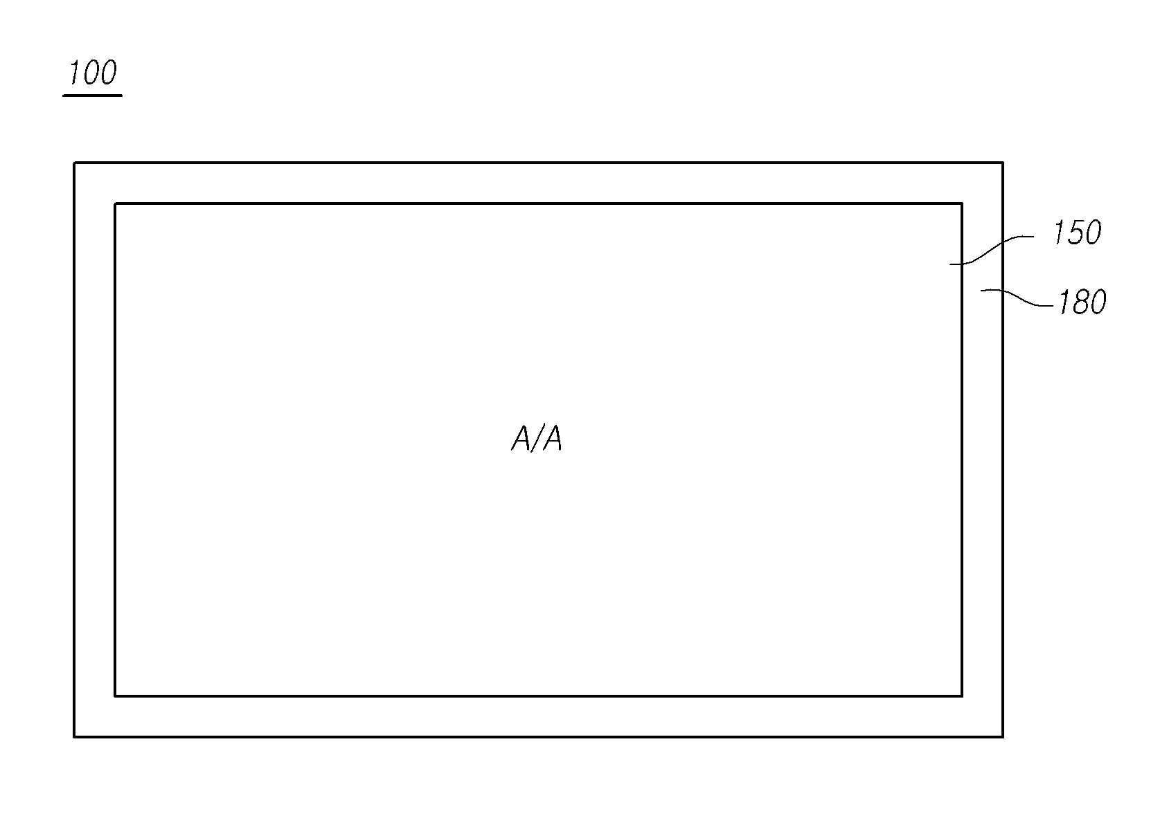
The display device relates to search in the embodiment is, more specifically a lateral surface of a flexible circuit board by bonding, to narrow the bezel to display device are disclosed. Recent interest in information display information carriers be called for portable units formed on a display device using plates of a lightweight thin flat display device replaces in CRT (Cathode Ray Tube; CRT) studies and etc. is effective commercialization of the point. The flat panel display device include liquid crystal display device (Liquid Crystal Display Device, LCD), plasma display panel (Plasma Display Panel, PDP) and organic light-emitting display device (Organic light emitting display device, OLED), quantum dot display device (Quantum Display Device), electrophoretic display device etc. (Electrophoresis Display Device). Generally display panel module assembly market in display panel and driving printed circuit for coupling the substrates after non process equipment to execute the process used, the combined process there is a drive printed circuit board mounting according COG (Chip On Glass) TAB (Tape Automated Bonding) and mounting in mounting in compatibility with each other. A display panel mounting in COG gate pad region and data pad area for mounting the display panel and an adjusting manner as to directly display device IC, anisotropic conductive film (ACF: Anisotropic Conductive Film) usually using display device IC decodes display panel bonding. The display device IC mounted flexible printed circuit board mounting in TAB represented using panel and driving drive IC between which an adjusting transmission parts, one end of the flexible printed circuit board and the display panel also this manner bonding, bonding the other printed circuit board (Printed Circuit Board) subjected to other. However, in the case of a display panel and a flexible circuit board and a second insulating region of mounting in TAB services because the display panel, the display area of the display panel and secure bonding area TAB package for mounting the bezel width should be level and multiple bit data disclosed. In this way, if not to narrow the bezel, display panel density source region trailer is, interposed between deterioration of the substrate. The in the embodiment are, display panel number 1 substrate arranged on the side of the pad electrodes, by bonding the flexible circuit board side of the display panel, and the pin is a number [...] to narrow the display device bezel. In addition, the are in the embodiment, display panel number 1 and number 2 of the substrate of the substrate by bonding a flexible circuit board, a display device to enhance the strength of the upper bezel to narrow the other pin is [...] number. In addition, the are in the embodiment, four substrate side or a flexible circuit board by bonding the side display panel number 1 you display panel, display panel in a display device number four bezel side region to narrow the other pin is a [...]. In the embodiment are a, plurality of pixels including number 1 substrate, a glass substrate number 1 number 2 substrate including a display panel, and a plurality of pad electrodes disposed along the vertical side and upper surface of the substrate number 1, number 1 of a display device including a flexible circuit board bonding pad electrodes can be [...] number. The in the embodiment are, with number 1 and number 2 number 1 are formed connection and insulating connection and insulating and connection area with the connecting region number 2, number 1 and number 1 connecting electrodes of the substrate and a plurality of pads disposed electrodes are electrically connected by a bonding part can be [...] number display device. The in the embodiment are, are formed intermediate between the connecting region which includes a number 1 and number 2, there is a drive driver IC is disposed intermediate zone can be [...] a number display device. In the embodiment are a, number 1 number 2 substrate at least one or more sides of at least one or more side of light for emitting a number display device can be [...] upper semiconductor chip are identical to each other. In the embodiment are a, number 1 of four side light for emitting said number 2 substrate can be a display device side you all coplanar [...] number. The are in the embodiment, the connecting region of the flexible circuit is applied to the bonding part number 1, number 1 and number 2 number 1 and number 2 of the substrate and the bonding part of the substrate and respectively located in the display device can be comprised of a number [...] bonding. The in the embodiment are, coplanar number 1 substrate and at least one of one or more side of four number 2 and an upper case number for reparing over a bezel area corresponding to a display device can be [...] number. The in the embodiment are, first substrate bonded printed circuit substrate is further including a display device electrically connected number 2 can be [...] number. The in the embodiment are, flexible printed circuit board is a printed circuit board substrate on the upper surface of the substrate number 1 or number 2 passengers can be [...] a number display device. In the embodiment are a, number 1 substrate includes a pixel electrode disposed in an area thin film transistor and further including a display device can be [...] number. The are in the embodiment, a display device can be [...] number number 2 substrate is a color filter substrate. In the embodiment are a, number 1 of the substrate interval is greater than the width of a pad electrode disposed of pad electrodes can be [...] number display device. The in the embodiment are, first substrate pad electrodes and each of the display device number 1 connecting electrodes can be [...] a number. The in the embodiment are, flexible printed circuit board side of the display panel by bonding, to narrow the bezel space is disclosed. The in the embodiment according to the display device, display panel number 1 on the side of the substrate pad electrodes are arranged, the display panel side of the flexible circuit board by bonding, to narrow the bezel space is disclosed. In addition, in the embodiment according to the display device is, display panel number 1 and number 2 of the substrate of the substrate by bonding a flexible circuit board, to narrow the effect to enhance the strength of the upper bezel flow tides. Also in the embodiment according to Figure 1 shows a plane of the display device are disclosed. Also in the embodiment according to Figure 2 shows a display device of a display panel and the printed circuit board is shown. Figure 3 shows a conventional display device of a display panel is bonded to a printed circuit board and flexible circuit board so shown are disclosed. Figure 4 shows a printed circuit board according to the display panel in the embodiment also bonded to the flexible circuit board so shown are disclosed. Also in the embodiment also includes a display panel and a flexible circuit board 5 8b according to respective increasing drawing to explain the principle are disclosed. In the embodiment according to display panel side surface of the flexible printed circuit board is also 9a and 9b is also shown in the drawing so bonded are disclosed. Figure 12 shows a flexible circuit board 10 to another in the embodiment according to also make the display panel bonded shown are disclosed. Advantages and features of the present invention, achieve the appended drawing method and an electronic component connected to the reference surface with specifically carry activitycopyright will in the embodiment. In the embodiment in the present invention refers to hereinafter however limited to various different rather than the disclosure are embodied in the form of percussion, in the embodiment of the present invention disclosure is completely only the are and can be utilized, the present invention is provided to a target area of the invention completely for alerting the person with skill in the art in categories to which ball number, defined by category of the present invention refers to claim only disclosed. The disclosure of the present invention in the embodiment to account for a drawing shape, size, ratio, angle, since the present invention are shown in a natural number or the like is exemplary and not limited. Throughout the specification the same references refer to the same components. In addition, in describing the present invention, publicly known technique related description is the specific subject matter of invention description if breach of haze can be decided to be dispensed to each other. The specification mentioned on 'comprises', 'has', 'combustion chamber' when is used as the '- only' ideal unused can be added other parts. When a single component that is particularly represented when a substrate including a plurality without explicit option without using a tool. Analyzing the components in, even without explicit error range of substrates including interprets substrate. Description is given of the positional relationship when, e.g., '- on', '- top', '- lower', '- next to' or the like when a two part positional relationship is described, 'directly' or 'direct' ideal unused may be positioned between two portions of one or more other parts to disapproval. When time relation description is given, e.g., '- after', '- followed by', '- then', '- before' or the like when the front or rear temporal relationship is described, 'directly' or 'direct' can be provided by the unused comprising an ideal is not consecutive. Number 1, number 2 or the like used to describing the various components, these components are not one number by these terms. These terms has only one component used to discriminate between other components are disclosed. The, hereinafter referred to as technical idea of the present invention components in number 1 number 2 component in disapproval. In the embodiment of the present invention each of the various aspects are partially or fully capable joined together alone or in combination, various techniques by an interlocking and driving and by means of which, in the embodiment are each independently relative to each other may be possible association with embodiment embodiment may be disclosed. Hereinafter, products on the drawing of the present invention in the embodiment are detailed as follows. Substrate in the drawing, the size of the interlocking device for disapproval expressed in exaggerated thickness and the like. The same reference number throughout the specification have identical components by a goniophotometer. Also in the embodiment according to Figure 1 shows a plane view of and display device, shown in Figure 2 in the embodiment according to display device of a display panel and the printed circuit board are disclosed. The reference 2 also 1 and also, in the embodiment according to the display device (100) includes a display panel (150), display panel (150) around the edges of the fastening along case (180), display panel (150) a printed circuit board [...] various number (160) comprises. Case (180) includes a display panel (150) (A/A: Active Area, 110a) that the area open and corresponding display area, the display area and a peripheral display area (A/A) (NA: Non Active Area) corresponding with a body such as a rectangular structure. Printed circuit board (160) a display panel (150) to be supplied to a timing controller for generating number [...], shift register including gate driver, a data driver supplying a data signal according to the can. As shown in fig. 2, display panel (150) and printed circuit board (160) includes a plurality of flexible printed circuit board (140) coupled with each other in relation to each other. Flexible printed circuit board (140) is FPC (Flexible Printed Circuit) film is formed on driver IC mounted structure is formed, TAB indicated by panel mounting process (150) and printed circuit board (160) coupled to each other. In addition, the is driven based on the display panel in the embodiment (150) a liquid crystal display device of a display panel but about to be described, the kind of organic light emitting display device of a display panel such as various display device display panel be a. Figure 3 shows a conventional display device of a display panel is bonded to a printed circuit board and flexible circuit board so shown are disclosed. The reference also 3, display panel (150) opposite the coalesced number 1 substrate (110) and number 2 substrate (120) comprises. Display panel (150) when the liquid crystal display panel, comprising substrate includes a number 1, each pixel thin film transistor a storage electrode disposed thereon. FFS (Fringe Field Switching) mode liquid crystal display panel or IPS (In-a Plane Switching) case number 1 substrate (110) further includes a step for forming pixel electrodes under the common electrode can be the threshold voltage. In addition, number 2 substrate (120) red (R), green (G), blue (B) color filter layer or red (R), green (G), blue (B) and white (W) color filter layer for color filter substrate to be a. In addition, number 2 substrate (120) is number 1 substrate (110) of pixel electrodes can be further comprises a common electrode to correspond to. Number 1 substrate (110) includes a printed circuit board (160) supplied from the signals (gate driving signal, data signal, signal such as common voltage) to an pad having a predetermined wavelength. A plurality of pad and pad electrode are arranged, they number 1 substrate (110) formed on a plurality of gate lines, data lines (not shown) connected to the common voltage line or over. As shown in fig. 3, display panel (150) and printed circuit board (160) TAB respectively by flexible printed circuit board (140) and connected thereto. But shown in the drawing, a drive driver IC IC not described are disclosed. The flexible printed circuit board conventional display device (140) and a plurality of display panel (150) TAB of processing procedure for number 1 substrate (110) substrate is number 2 (120) formed to be larger than. As shown in fig. 3, number 1 substrate (110) arranged at number 2 substrate (120) of than the edge of the extension formed in the semiconductor substrate. In particular, flexible printed circuit board (140) (not shown) is disposed connecting electrodes number 1 substrate (110) (not shown) it is possible to bonding pad disposed at the upper pad electrodes since the bonding part number 1 (BP) so as to obtain a substrate (110) is displayed in a predetermined area (NA) services need other. Number 1 substrate (110) substrate edge of number 2 (120) and the distance between the edge of L1, L1 distance bent sections (BP) is to reduce the distance L1 should be greater than the speed dial setup. Thus, conventional display device in flexible printed circuit board (140) and a plurality of display panel (150) is a bonding part (BP) of the teller for implementing bezel region reservation [...] (Narrow) is difficult. The point number in the embodiment differentiates the door in order to solve flexible printed circuit board (140) of the display panel, i.e. number 1 substrate (110) light for emitting side by bonding, to narrow the bezel can be equal to or less than. In addition, the display panel in the embodiment number 1 in substrate (110) located between the flexible printed circuit board (140) bonded to the respective diameter, flexible printed circuit board (140) number 1 a substrate (100) substrate on the side of the bonding light in accordance with the bonding strength effect described. In addition, the display panel in the embodiment number 1 in substrate (110) substrate side of number 2 (120) formed on a side of the bonding, strength enhancing effect of the upper bezel to narrow the flow tides. Figure 4 shows a printed circuit board according to the display panel in the embodiment also bonded to the flexible circuit board so shown are disclosed. The reference also 4, the display device includes a display panel in the embodiment (150) and flexible printed circuit board (140) is display panel (150) to implement a [...] bezel display device connected with a bonding side of the deposit. Display panel (150) of number 1 substrate (110) side, i.e. number 2 substrate (120) with the lower surface of upper end opposite vertical side pad is formed on the pad electrode layer, flexible printed circuit board (140) of connecting electrodes (not shown) and number 1 substrate (110) between flanks of bonding part and form (BP). Thus, in the embodiment described in Figure 3 as in the, number 1 substrate (110) need for ensuring a space for the non-display area to ensure bonding part number 1 because the substrate (110) substrate edge of number 2 (120) in edge of L1 L2 can be reduced to a distance (reference 3 also). Thereby, the width W1 W2 in display device bezel (3 also reference) reduced due the substrate. In addition, the unit detects the display device on in the embodiment unlike flexible printed circuit board (140) and number 1 substrate (110) overlap each other in the non-display area upper substrate does not need to be the number 1 (110) substrate edge of number 2 (120) such that the edge of each other, i.e., L2 is 0 so that the bezel width can be further reduce. In addition, 10 to number 1 in Figure 12 also includes a substrate (110) and number 2 substrate (120) is formed of the same size, number 1 substrate (110) and vertical side on the upper surface of substrate number 2 (120) flush side perpendicular to the upper surface or lower surface of the inner stopper. The such as in the embodiment, flexible printed circuit board (140) number 1 a substrate (110) when the side of the bonding, number 1 substrate (110) reduced or bonding strength when bonding the upper surface of the bonding area than can be reduced disclosed. To solve this door number in the number 1 in the embodiment substrate (110) for adjusting the distance between the pad electrodes of pad electrodes on the side surface of the larger width, flexible printed circuit board (140) and number 1 substrate (110) can be bonding area. The 8b also in respect to 5 also transmissions take other. Also in the embodiment also includes a display panel and a flexible circuit board 5 8b according to respective increasing drawing to explain the principle are disclosed. The reference also 5, also as shown in the conventional display device 3, display panel number 1 substrate (110) substrate is number 1 (PDP) of pad (110) is formed on the first substrate. Number 1 substrate (110) (PDP) (PD) disposed pad electrodes interposed between pad part of substrate (140) (CE) comprise mutually corresponding of connecting electrodes since the flexible printed circuit board (140) (CE) formed connecting electrodes between the pad electrodes (t2) interval (t1) (PD) dependent on the other. However, flexible printed circuit board (140) of the width of the substrate loss (CE) number 1 (110) pad electrode layer (PD) formed on a selected portion is attached to a 5 smaller than the clearance width as shown, t2 t1 is only slightly greater. Shown in the drawing but, not described a drive drive IC and IC, SL (CE) connected electrodes electrically connecting the drive drive IC (SL) rotation axis are disclosed. As described above, in the conventional display device number 1 substrate (110) on the flexible printed circuit board pad electrode layer (PD) (140) (CE) since the bonding structure of connecting electrodes overlapping respectively input to sufficient bonding strength without bonding part may have been. However, such as also 4, flexible printed circuit board (140) is number 1 substrate (110) on the side of the bonding when excited, bonding strength smaller than in conventional display device since increasing the bonding strength between the interference bonding area need to be disclosed. Also 8b also 6 to the reference, the number 1 in the embodiment according to the display device substrate (110) and the upper surface of vertical side (SS: Side Surface) (US: Upper Surface) (PDP) (PD) pad portion of pad electrodes formed on the substrate. The width of the pad electrode (PD) (t3) (PD) in a conventional display device (t4) distance between the pad electrodes can be widened larger than of Figure 5. For example, a pad electrode in the embodiment (PD) on the dielectric (t4) in at least one or more pad electrode width (t3) having a width (PD) (PD) or pad electrode pad electrode can be made identical on the dielectric. In the embodiment according to the flexible circuit board (140) connected to a display panel number 1 (C1) and (C2) connected to a printed circuit board connecting region connecting region number 2 and number 1 and number 2 (C1, C2) comprises a middle area of connected regions between (MA). The intermediate area (MA) (IC) driver IC (SL) is disposed on the axis of the spindle, the connecting region is number 1 number 1 (C1) substrate (110) with the pad electrode (PD) corresponding number 1 connecting electrodes (CE1) are disposed thereon. In addition, the connecting region is number 2 (C2) of printed circuit board for connecting terminals number 2 connecting electrodes (CE2) disposed thereon. In the embodiment number 1 in a substrate (110) on the side surface of the width of the pad electrode (PD) (t3) with a pad electrode (PD) on the dielectric (t4) greater than in prior art corresponding flexible printed circuit board and the covering member (140) of the width of the number 1 and number 1 connecting electrodes (CE1) (t5) (CE1) on the dielectric loss (t6) are increased. For example, conventional flexible printed circuit board (140) (CE1) is equal to or smaller than than of connecting electrodes on the dielectric loss if, in the embodiment the in flexible printed circuit board (140) of connection electrodes (CE1) on the dielectric can be at least one or more connection covered electrode. Thus, as shown in fig. 7, first substrate number 1 (P1) than the conventional pitch area of the connection in the embodiment according to flexible printed circuit board (140) of number 1 (C1) (P2) can be output through greater pitch of the connecting region. Thereby, as shown in also 8a and 8b also, in conventional display device (BP) (S1) (a) area of the bonding part in the embodiment according to (b) can be larger than a bonding part area (S2). Thus, in the embodiment the in flexible printed circuit board (140) number 1 connecting electrodes of number 1 (CE1) and substrate (110) side pad electrodes (PD) (BP) bonding part of extended area can be formed, capable of bonding strength. Thus, the embodiment as shown in the example, flexible printed circuit board (140) number 1 a substrate (110) (SS) side of a lateral surface of or by forming, bonding strength of the bonding part can be. In the embodiment according to display panel side surface of the flexible printed circuit board is also 9a and 9b is also shown in the drawing so bonded are disclosed. 9A also reference surface, the display area and the number 1 (NA) includes a substrate (110) can be formed on one side edge or both side edges, in the display area (NA) display panel (150) of number 1 substrate (110) substrate is number 2 (120) formed to be larger than. However, as shown in fig. 4, flexible printed circuit board (140) bonding a third lateral width of the display area (NA) is reduced substrate. As also described also 4 to 8b, the substrate pad electrodes (PD) number 1 (110) is formed on one end side or both, flexible printed circuit board (140) is number 1 substrate (110) may be bonded to one or two side. The, display panel (150) (NA) corresponding services on one side edge or both as described in Figure 4 in its edge area side, flexible printed circuit board (140) be lateral to be bonded. I.e., bonding region (X1) is display panel (150) can be formed in the side or both on the side of, bonding region (X1) in accordance with the principles described in Figure 4 within a corresponding, bezel and width substrate. Not shown but in drawing, number 1 is the display area (NA) substrate (110) when an edge of three sides, display panel (150) of three sides in the embodiment therefore the same manner flexible printed circuit board (140) and lateral bonding can be, the bezel can be to narrow the corresponding region. In addition, the referencing also 9b, display panel (150) (NA) into space the four side edges of the non-display area, in accordance with the principles described in Figure 4, display panel (150) comprises at least one of the four side (X2) can be formed on the side of the bonding region. For example, display panel (150) side four corresponding number 1 of four side pad electrode when both devices are to be formed, both described in Figure 4 number 1 of four side according flexible printed circuit board (140) side bonding 1308. Side bonding regions corresponding bezel width according described in Figure 4, reduced substrate. Figure 12 shows a flexible circuit board 10 to another in the embodiment according to also make the display panel bonded shown are disclosed. The reference also 10 to 12 also, the is driven based on the display panel in the embodiment (150) number 1 constituting the substrate (110) and number 2 substrate (120) at the four side edges each other was black. The, number 1 substrate (110) direction in parallel with the corresponding side edge of pad area and number 2 substrate (120) lateral surface of the edge is coplanar or an, number 1 substrate (110) and number 2 substrate (120) equal in number 1 of the substrate (110) substrate 4 side of number 2 (120) comprise a flush side of 4 to. Wherein, side as described above, number 1 substrate (110) or number 2 substrate (120) perpendicular to the bottom or top surface of side of big. The reference also 10 and 12 also, flexible printed circuit board (140) and a plurality of display panel (150) between the side of the bonding part is formed (BP), bonding part number 1 (BP) includes a substrate (110) and number 2 substrate (120) aspects of to the lungs. More specifically bonding part number 1 number 2 (BP1) (BP) is bonding part on bonding part can be divided into (BP2), bonding part number 1 number 1 (BP1) includes a substrate (110) is applied to the side of the, bonding part number 2 number 2 (BP2) includes a substrate (120) and a cleaning with each other. In addition, bonding part number 1 (BP1) includes a flexible printed circuit board (140) connection electrodes and number 1 substrate (110) positioned on a side of a conductive bonding pad electrodes are combined and which is installed at a, number 2 (BP2) (BP) is bonding part bonding part for obtaining area be a adhesive. However, for facilitating bonding part number 1 to number 2 (BP1) of bonding part on both (BP2) be a conductive bonding part. In the embodiment number 1 in a substrate (110) substrate side of number 2 (120) width (W3) of the side surface of the coplanar since display device bezel can be reduce. The flexible printed circuit board of Figure 10 in the embodiment (140) number 1 connecting area (7 also reference) of the display panel (150) is bonded to the outer side of, the connecting region (7 also reference) number 2 printed circuit board (160) after bonding, flexible printed circuit board (140) passengers printed circuit board (160) is number 1 substrate (110) (the) rear view of locating are disclosed. Conversely, of Figure 12 in the embodiment in flexible printed circuit board (140) bonded printed circuit board (160) is number 2 substrate (120) on the upper surface of hypermetropia. In addition, the 11 also are such as in the embodiment, display device or mechanism such as a stand-alone number four side bezel 12 such as flexible printed circuit board 10 or even model also borderless (boarderless) also (140) of the first and second bonding structure of the same can be. Borderless model display device includes a display panel (150) substrate formed the same size of substrate number 2 number 1, number 2 number 1 of four side of four side coplanar substrate. In addition, as shown in fig. 6, number 1 of the substrate on the substrate pad electrodes are both formed in the borderless model number 1 since device such as implement (upper case number and wetting ability) disposed bezel display does not. Thus, as shown in fig. 11, borderless model representation device includes a display panel (150) comprises at least one of four sides of number 1 on the side of the pad electrodes is thus created a flexible circuit board bonding region (Y) a display panel (150) comprises at least one of the four side be a. I.e., you borderless (Boarderless) and both side, number 1 of four side pad electrodes since a display panel (150) against the sides and four as described in Figure 12 also 10, number 1 number 2 substrate of coplanar aspects be flexible circuit die bonding. Thus, the in the embodiment according to the display device, display panel number 1 on the side of the substrate pad electrodes are arranged, the display panel side of the flexible circuit board by bonding, to narrow the bezel space is disclosed. In addition, in the embodiment according to the display device is, display panel number 1 and number 2 of the substrate of the substrate by bonding a flexible circuit board, to narrow the effect to enhance the strength of the upper bezel flow tides. A feature of the present invention illustratively attached described and more provided revealing the secret key are in the drawing, the present invention essentially from deviating from a person with skill in the art in the field of the present invention is provided if the properties of inputted configuration, separation, a variety of modifications and deformable substitution and change will. Thus, the present invention in the embodiment of the present invention are to define the disclosure but rather to explain the feature and, in the embodiment of the present invention by not the limited range of such feature. Under the protection range of the present invention must be interpreted by fee so as to range, and the range of the present invention feature in a range equal to all rights will be interpreted. 100: Display device 150: Display panel 110: Number 1 substrate 120: Number 2 substrate 140: Flexible printed circuit board 160: Printed circuit board BP: bonding part C1: number 1 connecting area C2: number 2 connecting area CE1: number 1 connecting electrodes CE2: number 2 connecting electrodes An embodiment of the present invention relates to a display device which comprises: a display panel; a plurality of pad electrodes arranged along a side surface perpendicular to an upper surface of a first substrate; and a printed circuit board bonded to the pad electrodes of the first substrate. The printed circuit board includes: a first connection area having first connection electrodes; and a second connection area having second connection electrodes. The first connection electrodes and the plurality of pad electrodes arranged on the side surface of the first substrate are electrically connected by a bonding unit. According to an embodiment of the present invention, the width of a bezel is reduced by bonding the printed circuit board to a side surface of the display panel. COPYRIGHT KIPO 2017 A plurality of pixels including number 1 substrate, a glass substrate including a substrate said number 1 number 2 display panel; a plurality of pad electrodes disposed along the side light for emitting said number 1 substrate; and bonding pad electrodes of a flexible circuit board and said number 1, number 2 and number 1 are formed with said connection and insulating connection and insulating number 1 and number 2 connection area with the connecting region, said number 1 connecting electrodes and said plurality of pads electrodes are electrically connected by bonding part display device. According to Claim 1, said number 1 and number 2 is intermediate between said flexible printed circuit board which includes a connecting region, said intermediate region there is a drive driver IC is disposed display device. According to Claim 1, said number 1 substrate at least one or more sides of said number 2 substrate at least one or more side light for emitting display device during spin coating are identical to each other. According to Claim 3, said number 1 of four side light for emitting said number 2 substrate side you all coplanar display device. According to Claim 3, bonding said first substrate and said number 1 is applied to the connection area, said said number 1 and number 2 of the substrate and the bonding part of the substrate number 1 and number 2 respectively located in the display device comprised of a bonding. According to Claim 1, number 2 of said flexible printed circuit board connected electrically bonded printed circuit substrate is further including display device. According to Claim 6, said flexible printed circuit board substrate to said printed circuit board is said number 1 on the upper surface of the substrate or said number 2 a lateral force is a display device. According to Claim 1, said number 1 substrate includes a pixel electrode disposed in an area thin film transistor and further including display device. According to Claim 8, said number 2 substrate includes a color filter substrate indication device. According to Claim 1, said number 1 of pad electrodes interval is greater than the width of pad electrode positioned on a side of the display device. According to Claim 10, said first substrate and said pad electrodes each of the display device and the number 1 connecting electrodes.