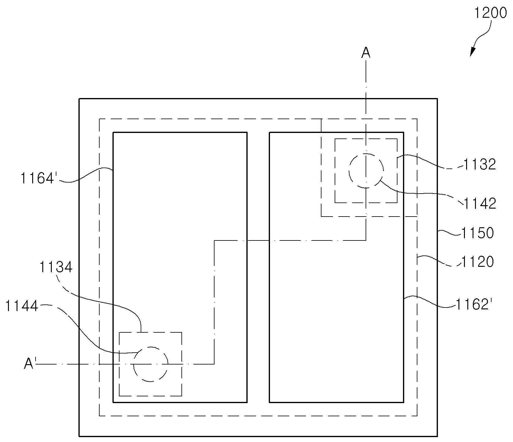
LIGHT EMITTING DIODE PACKAGE
The present invention refers to the delay unit are disclosed. Light emitting diode is basically the N type semiconductor junctions are P-type semiconductor and a PN junction diode are disclosed. Said light emitting diode includes a P-type semiconductor and N type semiconductor sample behind, said P-type semiconductor and N type semiconductor by applying voltage to the emitting surface, said P-type semiconductor and said N type semiconductor moves toward the hole, with a reduced size of said P type semiconductor migrates towards the said PN said N type semiconductor the electrons of electrons and holes to move to a junction with each other. The conduction band electrons (conduction band) to (valence band) is moved to said PN junction in combination with consumer falls into hole while to be coated. The, capable of supporting said conductive appliance height difference i.e., to dissipate energy as long as a pulse corresponding to the difference energy, said energy in the form of light emitted into the substrate. Using said first growth substrate generally LED package may include a light emitting diode having one side of the light emitting diode chip is formed on a growth substrate, said light emitting diode chip package rear light emitting diode package. E.g. flip-chip light emitting light emitting diode is formed on the light emitting diode chip for number bath is provided to increase growth substrate is formed, said light emitting diode chip to a submount or the like mounted on a bottom surface, said submount mounted flip chips packaged light emitting flip-chip light emitting high pressure liquid coolant arranging his number. The number of the existing method LED package may include a light emitting diode chip and the reaction step of packaging an annealing tank fill the trench by high well as well as a complicated process, the pin is point number number tank cost door sizes. In addition, number of the existing method LED package may include a growth substrate on the light emitting diode chip and high pressure liquid coolant, such as packaged chip to a submount by LED package may include a main frame to near the coverage like mobile number by each number point at the door that has been applied. In addition, in one aspect of the existing method LED package may include a phosphor layer through the phosphor converted light is extracted from light which has not been converted through optical properties that number to control his point at the door. In addition, the resultant structure of the existing method LED package may include a light emitted diode chips the reverse door been measured number. In addition, when the resultant structure of the existing method LED package may include a light emitting diode chip, as well as difficult to heat activation pin is difficult to door number point (current spreading). In addition, number of the existing method LED package may include a light emitting diode chip packaging process of annealing the fill tank made of high well as well as complex process, number tank cost door sizes has been measured number. The purpose of the invention to small number of wafer level packaging process number the light emitting diode light emitting diode ramp of a number number bath method are disclosed. It is another object of the present invention light which has not been extracted through conversion phosphor layer at the side of the light emitting diode package to prevent or reduce the number of light emitting diode number bath method are disclosed. Of the present invention another object is to provide a cathode made of an light emitting diode package and method for number bath large number method are disclosed. Another object of the present invention easily dissipated current hereinafter for light emitting diode package and method for number bath method a large number are disclosed. As well as the data of the present invention another object is to provide a low-defect, number tank costs are low comprises a light emitting diode package and method for number bath a number method are disclosed. In order to achieve said purposes, according to one aspect of the present invention, number 1-type semiconductor layer, number 2-type semiconductor layer, said number 1 and number 2 type semiconductor layer including an active layer located between contacts semiconductor structure layer; said either one of the five [mik cone [thayk layer number 2-type semiconductor layer on a semiconductor structure; said five [mik cone [thayk layer located on the number 2 pad; said said number 2 is partially covering the pad, said number 2 opening opening a pad insulating film including number 1 number 1; and said number 1 through an opening in the insulating layer electrically or thermally connected contact said number 2 number 1 and number 2 interconnection, said number 1 DBR layer insulation film including light emitting diode package is encoded ball number. According to one aspect of the present invention another, substrate; said substrate on one side of the is equipped, number 1-type semiconductor layer, an active layer and a number 2 n type semiconductor layer including semiconductor structure layer; said number 1 and number 2 number 1 and number 2 with bump-type semiconductor layer to the second-type semiconductor layer; a protective layer covering at least said semiconductor structure layer; and said protective layer is provided on, said number 1 and number 2 number 1 and number 2 including light emitting diode package is encoded using bump pad are each coupled bump ball number. Said substrate is side edge can be warp. The other side of said LED package may include a phosphor layer on said substrate can be. The substrate can be said other side of the pattern. Said protective layer consists of said number 1 and number 2 surrounding the bumps can be. Said protective layer consists of said number 1 and number 2 can be expose a portion of the bump. Said number 1 and number 2 bumps each having a plurality can be. Said number 1 and number 2 number 1 and number 2 each of said LED package may include a bump pads and substrate (substrate) having one side electrode on the surface; and said number 1 and number 2 and number 1 and number 2 have a bump pad electrically connecting the conductive bonding material can be. Said conductive bonding material is either one of the front side thereof can covering at least part of said semiconductor structure. Said conductive bonding material is said protective layer covers at least a portion of a side of the thereof can. Said conductive bonding material is said thereof can covers at least a portion of the substrate. Number 1 and number 2 which said conductive bonding material is conductive adhesive conductive adhesive, conductive bonding material is said number 1 and electrically connected to the bump pad and said number 1, said number 2 and electrically connected to the bump pad and conductive bonding material is said number 2, said number 1 and number 2 spaced apart conductive bonding material is conductive joint material thereof can. Said LED package may include a semiconductor structure is provided on said layer, said number 2 number 1 opening and exposing said number 1 type semiconductor layer exposing openings can be conductive silicon type semiconductor layer number 2. Said LED package may include said protruded is equipped, said number 1 through an opening in the number 1 type semiconductor layer that contacts the contact pads and said number 2 number 1 through an opening in the number 2 type semiconductor layer that contacts the contact pad number 2 can be. Said LED package may include a protective layer is provided on said, with number 1 and number 2 current diffusion layer and said number 2 number 1 bump pad between said number 1 bumps with number 2 can be between bump pad bump with current spreading layer. According to the present invention, the LED chip number number of wafer level packaging process to small number of ramp bath method number equal to or less than a light emitting diode. In addition, according to the present invention, light which has not been extracted through conversion phosphor layer at the side of the light emitting diode package to prevent or reduce the number of light emitting diode number equal to or less than bath method. In addition, according to the present invention, a large number of cathode made of an light emitting diode bath method number equal to or less than. In addition, according to the present invention, hereinafter heat for a large number of light emitting diode current easily dispersible bath method number equal to or less than. In addition, according to the present invention, as well as defect formed in low, number tank costs are low comprises a light emitting diode package and method for number bath method a number equal to or less than. According to one embodiment of the present invention example shown in Figure 1 shows a cross-section of the light emitting also are disclosed. Figure 3 shows a plane view of the present invention according to another embodiment of the light emitting example also 2 and also shown and cross section are disclosed. Figure 5 shows a plane view of the present invention according to another embodiment of the light emitting example also 4 and also shown and cross section are disclosed. Figure 6 shows a cross-section according to another embodiment of the present invention shown in the example of the light emitting also are disclosed. Figure 8 shows a plane view of the present invention according to another embodiment of the light emitting example also 7 and also shown and cross section are disclosed. Figure 10 shows a plane view of the present invention according to another embodiment of the light emitting example also 9 and also shown and cross section are disclosed. Figure 11 shows a example of the present invention according to another embodiment of the light emitting plane shown also are disclosed. Figure 12 shows a example of the present invention according to another embodiment also shown in the plane of lines electrically connect light emitting diode package are disclosed. Figure 13 shows a cross-section according to another embodiment of the present invention shown in the example of the light emitting also are disclosed. Figure 14 shows a example of the present invention according to another embodiment of the light emitting plane shown also are disclosed. Figure 15 shows a example of the present invention according to another embodiment of the light emitting plane shown also are disclosed. Figure 17 shows a plane view according to another embodiment of the present invention example 16 and also the light emitting circuit shown and also are disclosed. Figure 19 shows a plane view according to another embodiment of the present invention example 18 and also of the light emitting circuit shown and also are disclosed. According to one embodiment of the present invention to Figure 27 shows a light emitting diode package number bath method example 20 also also is shown cross-section are disclosed. Figure 38 shows a method embodiment of the present invention also 28 to another light emitting diode package according to example number bath also is shown cross-section are disclosed. Figure 41 shows a method of the present invention according to another embodiment also 39 to light emitting diode package number bath is shown in cross-section also are disclosed. Hereinafter, the present invention according to embodiment examples with reference to the attached drawing detailed the on-sensors other. According to one embodiment of the present invention example shown in Figure 1 shows a cross-section of the light emitting also are disclosed. With reference to the SFC also 1, according to one embodiment of the present invention example light emitting diode package (1100) substrate (1110), semiconductor structure layer (1120), the contact pads (1130), bumps (1140), protective layer (1150) and bump pads (1160) can be comprising. In addition, said light emitting diode package (1100) phosphor layer (1170), passivation layer (1180) and current dispersion layer (1190) can be further. The, said phosphor layer (1170), passivation layer (1180) and the activation layers (1190) may be omitted thereby preventing any disapproval. Said substrate (1110) may be the growth substrate, said sapphire substrate growth substrate, such as silicon carbide substrate or silicon substrates can be a, preferably said sapphire substrate be a growth substrate. Said substrate (1110) is on the surface on one side to said semiconductor structure layer (1120), the contact pads (1130), bumps (1140), protective layer (1150) and bump pads (1160) can be sequentially with. Said substrate (1110) is on the other side (1112) (not shown) to collector eye pattern (not shown) such as local or blast with an uneven patterns for increasing light extraction efficiency can be. In addition said substrate (1110) is inclined side edge (1114) can be with. Said side inclination (1114) is said substrate (1110) side of change height light extraction efficiency can be serves. According to one embodiment of the present invention example light emitting diode package (1100) is said substrate (1110) provided on one side of the semiconductor structure layer (1120) emitting light to said substrate (1110) extracting shape on the other side direction can be. Said collector eye pattern (not shown) or local (not shown) such as an uneven patterns are blast said substrate (1110) drawn on the other side of the light direction light extraction efficiency could be bonded each other. Said semiconductor structure layer (1120), particularly active layer (1124) light emits light in said substrate (1110) when the other side of the extracting direction, said light said substrate along said path of travel of light (1110) does not cause total reflection at the other side of the beam of light can be extracted, said collector eye pattern (not shown) such as an uneven patterns (not shown) local blast or the substrate (1110) in said other side of the encapsulating substrate reduces light (1110) by a sampling probability of the other side of the light emitting diode package (1100) light extraction efficiency of the height could be bonded each other. On the other hand, said substrate (1110) on the other side of the, preferably said semiconductor structure layer (1120) extracted light emits light in said substrate (1110) has a plurality of said phosphor layer (1170) can be with. Said phosphor layer (1170) is said semiconductor structure layer (1120) by emitting light with wavelength converting effect serves, said phosphor layer (1170) comprising the phosphor material for converting the wavelength of emitted light can be. Said semiconductor structure layer (1120) is number 1-type semiconductor layer (1122), active layer (1124) and number 2-type semiconductor layer (1126) can be comprising, said substrate (1110) and number 1-type semiconductor layer (1122) buffer layer (not shown) can be between with. Said buffer layer (not shown) is said substrate (1110) and number 1-type semiconductor layer (1122) with lattice mismatch between order can be. In addition, said buffer layer (not shown) can be composed of one or more single layer, which comprises a when, high temperature buffer layer can be composed of low temperature buffer layer. Said number 1-type semiconductor layer (1122) is said substrate (1110) can be provided on, as shown in part 1 also can be employed to reduce the shape, this said active layer (1124) and number 2-type semiconductor layer (1126) can be exposed by etching a portion of the mesa. Said mesa etch said number 1-type semiconductor layer (1122) 1308.-resist. Said number 1-type semiconductor layer (1122) is number 1-type impurity, for example N-type impurity doped (Al, In, Ga) N-based group III can be formed and made of a nitride semiconductor, said number 1-type semiconductor layer (1122) can be single layer or be multi-layered. For example, said number 1-type semiconductor layer (1122) comprising the can be. Said active layer (1124) is said number 1-type semiconductor layer (1122) can be provided on, said active layer (1124) can be composed of one or more single layer. In addition, said active layer (1124) (not shown) may be a single quantum well structure including a well layer one and, well layer (not shown) and barrier layer (not shown) is formed by alternating laminated structure can be comprised of a multiple quantum well structure. The, said well layer (not shown) or a barrier layer (not shown) each or both superlattice structures can be made. Said number 2-type semiconductor layer (1126) is said active layer (1124) can be provided on, said number 2-type semiconductor layer (1126) the number 2-type impurity, for example, P-type impurity doped (Al, In, Ga) made of a nitride semiconductor can be formed N-based group III, said number 2-type semiconductor layer (1126) can be single layer or be multi-layered. For example, said number 2-type semiconductor layer (1126) comprising the can be. In addition, said semiconductor structure layer (1120) is said active layer (1124) and number 2-type semiconductor layer (1126) (not shown) can be between blocking layer comprising. Said blocking layer (not shown) can be made by the electron recombination efficiency, with relatively wide bandgap element consisting of a material can be. Said blocking layer (not shown) is made of a nitride semiconductor-based group III (Al, In, Ga) N can be formed, for example, AlGaN can be included. Said passivation layer (1180) is said semiconductor structure layer (1120) with the substrate (1110) can be provided on. Said passivation layer (1180) is lower said semiconductor structure layer (1120) serve as external protect it from the environment, with an insulating layer including silicon oxide layer can be. Said passivation layer (1180) mesa etching the exposed said number 1-type semiconductor layer (1122) exposing part of the surface of opening number 1 (1182) and said number 2-type semiconductor layer (1126) exposing part of the surface of opening number 2 (1184) can be with. Said contact pads (1130) number 1 the contact pads (1132) and number 2 contact pads (1134) can be a. Said number 1 contact pads (1132) includes opening said number 1 (1182) a-type semiconductor layer are exposed through said number 1 (1122) can be made by contact with. Said number 2 contact pads (1134) includes opening said number 2 (1184) a-type semiconductor layer are exposed through said number 2 (1126) can be made by contact with. The, said passivation layer (1180) if the number 1 having contact pads (1132) and number 2 contact pads (1134) each said number 1-type semiconductor layer (1122) and number 2-type semiconductor layer (1126) can be made by contact with a predetermined position of said semiconductor layer. The, even thought it does not also shown in, said number 2-type semiconductor layer (1126) is the top number 2 number 2 (not shown) comprising heavily doped-type impurities can be high concentration doping-type semiconductor layer, said number 2-type semiconductor layer (1126) contact pads and said number 2 (1134) (not shown) for further include a past between ohmic contact may be filled. Said contact pads (1130) is Ni, Cr, Ti, Al, like Ag or Au can be done via the disclosed. Said (not shown) past the ITO, IZO or ZnO TCO contact material such as Ni/Au on such as can be done via the disclosed. Said bumps (1140) is number 1 bump (1142) and number 2 bump (1144) can be a. Said number 1 bump (1142) said number 1 has contact pads (1132) can be provided on, said number 2 bump (1144) said number 2 includes contact pads (1134) can be provided on. Said bumps (1140) comprising the Au can be. On the other hand, said bumps (1140) (Stud Bump) may be stud bump is formed, said bumps (1140) substrate and or coating formed paired etching selectively the disapproval. Said protective layer (1150) is said substrate (1110) equipped on, at least said semiconductor structure layer (1120) protect the covering of the week. For example, as shown in said substrate also 1 (1110) semiconductor structure layer provided on a predetermined region (1120) as well as protect the surface of side are also used for. Said protective layer (1150) silicone-based oxide, and may be made from an inorganic substance such as silicone nitride, disapproval made of organic material such as resin. Said current spreading layers (1190) is said protective layer (1150) is provided on, said bumps (1140) toward the supporting part can be electrically connected. Said current spreading layers (1190) is said bump pads (1160) is said protective layer (1150) with the substrate (1110) used to push on, for hereinafter with respect to serve as to eliminate the disapproval. Said current spreading layers (1190) current spreading layer the number 1 (1192) and number 2 current spreading layer (1194) which, said number 1 current spreading layer (1192) is said number 1 bump (1142) electrically connected with a, said number 2 current spreading layer (1194) is said number 2 bump (1144) toward the supporting part can be electrically connected. Said current spreading layers (1190) is Ni, Cr, Ti, Al, like Ag or Au can be done via the disclosed. Said bump pads (1160) is said current spreading layers (1190) can be provided on. I.e., said bump pads (1160) bump pad the number 1 (1162) and number 2 bump pad (1164) can be made, said bumps (1140) toward the supporting part can be electrically connected. Said bump pads (1160) is said bumps (1140) comprising Au can be equal. The, said number 1 bump pad (1162) and number 2 bump pad (1164) each said number 1 current spreading layer (1192) and number 2 current spreading layer (1194) may be comprised of a smaller size than the size of, said number 1 contact pads (1132) and number 2 contact pads (1134) may also be used but provided with a smaller size than the size of an, is not limited. I.e., said number 1 bump pad (1162) and number 2 bump pad (1164) each said number 1 current spreading layer (1192) and number 2 current spreading layer (1194) may be may be slightly greater than the size of the same, said number 1 contact pads (1132) and number 2 contact pads (1134) may be slightly greater than the size of an, same as the disapproval. Thus, according to one embodiment of the present invention example light emitting diode package (1100) substrate (1110) on semiconductor structure layer (1120), the contact pads (1130) and bumps (1140) having, at least said semiconductor structure layer (1120), preferably said semiconductor structure layer (1120), the contact pads (1130) and bumps (1140) protective layer protecting (1150) having, said protective layer (1150) on said bumps (1140) connected electrical bump pads (1160) whereby, said semiconductor structure layer (1120) packaging forming substrate itself, i.e., packaged wafer level, not requiring separate package process, thereby the light emitting number can be small in its size. Figure 3 shows a plane view of the present invention according to another embodiment of the light emitting example also 2 and also shown and cross section are disclosed. The, Figure 3 shows a A provided A ' along a line cut of cross-sectional drawing which illustrates, also Figure 2 shows said substrate (1110) one side of the plane of Figure 2 look direction are disclosed. Also 3 2 and also with reference to the described, other embodiment of the present invention example according to light emitting diode package (1200) according to one embodiment of the present invention described with reference to example 1 also includes a light emitting diode package (1100) in the ratio of bump pads (1160) provided in both configuration and the minimum without performing the configuration identical to the other and therefore the description, difference bump pads (1160) only for illustrating each other. I.e., other embodiment of the present invention example according to light emitting diode package (1200) substrate (1110), semiconductor structure layer (1120), the contact pads (1130), bumps (1140), protective layer (1150) and bump pads (1160) can be comprising. In addition, said light emitting diode package (1200) is not shown but in mobilities, also 1 described with reference to a light emitting diode package (1100) defined in the phosphor layer (1170), passivation layer (1180) and current dispersion layer (1190) can be further. The, said phosphor layer (1170), passivation layer (1180) and the activation layers (1190) is off disagreement and not shown. In addition, said light emitting diode package (1200) is said substrate (1110) on the other side (1112) (not shown) to collector eye pattern (not shown) such as local or blast with an uneven patterns for increasing light extraction efficiency can be, said substrate (1110) and number 1-type semiconductor layer (1122) buffer layer (not shown) can be between having, said active layer (1124) and number 2-type semiconductor layer (1126) (not shown) can be between blocking layer with, said number 2-type semiconductor layer (1126) and number 2 contact pads (1134) number 2 (not shown) and contact (not shown) between high concentration doping with can-type semiconductor layer. Said bump pads (1160) is also shown in 2 and 3 also as light emitting diode package (1200) one side of, said substrate (1110) provided on one side of the protective layer (1150) can be provided on the surface of. The, said bump pads (1160) bump pad the number 1 (1162 ') and number 2 bump pad (1164') can be a, said number 1 bump pad (1162 ') and number 2 bump pad (1164') is the same size said protective layer (1150) can be provided on. In particular, as also shown in said number 1 2 bump pad (1162 ') and number 2 bump pad (1164') is said semiconductor structure layer (1120) may be provided in a region corresponding to, but not shown in Figure 2 is the, said protective layer (1150) covers the entire surface of shape disapproval. I.e., 2 and 3 are also shown in light emitting diode package (1200) number 1 of bump pad (1162 ') and number 2 bump pad (1164') 1 also includes a light emitting diode package shown in (1100) number 1 of bump pad (1162) and number 2 bump pad (1164) than a size higher than said light emitting diode package (1200) are mounted can be fitted for other device when hereinafter. Figure 5 shows a plane view of the present invention according to another embodiment of the light emitting example also 4 and also shown and cross section are disclosed. The, Figure 5 shows a B provided B ' along a line cut of cross-sectional drawing which illustrates, Figure 4 shows a also said substrate (1110) one side of the plane of Figure 4 as seen direction are disclosed. Also 4 and 5 also with reference to the described, according to another embodiment of the present invention example light emitting diode package (1300) according to embodiment 3 of the present invention is also described with reference to example 2 and also other light emitting diode package (1200) also on the contact pads (1130) provided in both configuration and the minimum without performing the configuration identical to the other and therefore the description, the contact pads difference (1130) only for illustrating each other. I.e., according to another embodiment of the present invention example light emitting diode package (1300) substrate (1110), semiconductor structure layer (1120), the contact pads (1130), bumps (1140), protective layer (1150) and bump pads (1160) can be comprising. In addition, said light emitting diode package (1200) is not shown but in mobilities, also 1 described with reference to a light emitting diode package (1100) defined in the phosphor layer (1170), passivation layer (1180) and current dispersion layer (1190) can be further. The, said phosphor layer (1170), passivation layer (1180) and the activation layers (1190) was dispensed. In addition, said light emitting diode package (1200) is said substrate (1110) on the other side (1112) (not shown) to collector eye pattern (not shown) such as local or blast with an uneven patterns for increasing light extraction efficiency can be, said substrate (1110) and number 1-type semiconductor layer (1122) buffer layer (not shown) can be between having, said active layer (1124) and number 2-type semiconductor layer (1126) (not shown) can be between blocking layer with, said number 2-type semiconductor layer (1126) and number 2 contact pads (1134) number 2 (not shown) and contact (not shown) between high concentration doping with can-type semiconductor layer. Said contact pads (1130), in particular number 2 contact pads (1134') 4 and 5 also is also as shown in said number 2-type semiconductor layer (1124) can be shape covering the surface of the wider. The example of the present invention light emitting diode package according to another embodiment (1300) is wide number 2 contact pads (1134 ') said number 2 having contact pads (1134') number 2 the multi-bump (1144) can be with. In addition said number 1 contact pads (1132') also permitting electrons to a plurality of number 1 bump (1142) with disapproval. Figure 6 shows a cross-section according to another embodiment of the present invention shown in the example of the light emitting also are disclosed. 6 Also with reference to the described, according to another embodiment of the present invention example light emitting diode package (2100) includes a growth substrate (2110), semiconductor structure layer (2120), the contact pads (2130), bumps (2140), protective layer (2150), bump pads (2160), substrate (substrate) (2210), electrodes (2220) and conductive adhesive (2230) can be comprising. In addition, said light emitting diode package (2100) phosphor layer (2170), passivation layer (2180) and the pad protective layer (2190) can be further. The, said phosphor layer (2170), passivation layer (2180) and the pad protective layer are (2190) may be omitted thereby preventing any disapproval. Said growth substrate (2110) sapphire substrate, such as silicon carbide substrate or silicon substrates can be a, preferably said sapphire substrate be a growth substrate. Said growth substrate (2110) is on the surface on one side to said semiconductor structure layer (2120), the contact pads (2130), bumps (2140), protective layer (2150) and bump pads (2160) can be sequentially with. Said growth substrate (2110) is on the other side (2112) (not shown) to collector eye pattern (not shown) such as local or blast with an uneven patterns for increasing light extraction efficiency can be. In addition said growth substrate (2110) is inclined side edge (2114) can be with. Said side inclination (2114) is said growth substrate (2110) side of change height light extraction efficiency can be serves. According to another embodiment of the present invention example light emitting diode package (2100) includes said growth substrate (2110) provided on one side of the semiconductor structure layer (2120) emitting light to said growth substrate (2110) extracting shape on the other side direction can be. Said collector eye pattern (not shown) or local (not shown) such as an uneven patterns are said blast growth substrate (2110) direction other side of the light extracted by the light extraction efficiency height could be bonded each other. Said semiconductor structure layer (2120), particularly active layer (2124) light emitting said growth substrate (2110) when the other side of the extracting direction, said light along said path of travel of light said growth substrate (2110) does not cause total reflection at the other side of the beam of light can be extracted, said collector eye pattern (not shown) such as an uneven patterns (not shown) local blast or the growth substrate (2110) encapsulating the light reduces in the other side of the growth substrate (2110) by a sampling probability of the other side of the light emitting diode package (2100) light extraction efficiency of the height could be bonded each other. On the other hand, said growth substrate (2110) on the other side of the, preferably said semiconductor structure layer (2120) extracted light emits light in said growth substrate (2110) has a plurality of said phosphor layer (2170) can be with. Said phosphor layer (2170) is said semiconductor structure layer (2120) acts by transforming the light emitting wavelength of emitted light, said phosphor layer (2170) comprising the phosphor material for converting the wavelength of emitted light can be. Said semiconductor structure layer (2120) is number 1-type semiconductor layer (2122), active layer (2124) and number 2-type semiconductor layer (2126) can be comprising, said growth substrate (2110) and number 1-type semiconductor layer (2122) (not shown) can be between having a buffer layer. Said buffer layer (not shown) is said growth substrate (2110) and number 1-type semiconductor layer (2122) with lattice mismatch between order can be. In addition, said buffer layer (not shown) can be composed of one or more single layer, which comprises a when, high temperature buffer layer can be composed of low temperature buffer layer. Said number 1-type semiconductor layer (2122) is said growth substrate (2110) can be provided on, as shown in part 1 also can be employed to reduce the shape, this said active layer (2124) and number 2-type semiconductor layer (2126) can be exposed by etching a portion of the mesa. Said mesa etch said number 1-type semiconductor layer (2122) 1308.-resist. Said number 1-type semiconductor layer (2122) is number 1-type impurity, for example N-type impurity doped (Al, In, Ga) N-based group III can be formed and made of a nitride semiconductor, said number 1-type semiconductor layer (2122) can be single layer or be multi-layered. For example, said number 1-type semiconductor layer (2122) comprising the can be. Said active layer (2124) is said number 1-type semiconductor layer (2122) can be provided on, said active layer (2124) can be composed of one or more single layer. In addition, said active layer (2124) (not shown) may be a single quantum well structure including a well layer one and, well layer (not shown) and barrier layer (not shown) is formed by alternating laminated structure can be comprised of a multiple quantum well structure. The, said well layer (not shown) or a barrier layer (not shown) each or both superlattice structures can be made. Said number 2-type semiconductor layer (2126) is said active layer (2124) can be provided on, said number 2-type semiconductor layer (2126) is number 2-type impurity, for example, P-type impurity doped (Al, In, Ga) made of a nitride semiconductor can be formed N-based group III, said number 2-type semiconductor layer (2126) can be single layer or be multi-layered. For example, said number 2-type semiconductor layer (2126) comprising the can be. In addition, said semiconductor structure layer (2120) is said active layer (2124) and number 2-type semiconductor layer (2126) (not shown) can be between blocking layer comprising. Said blocking layer (not shown) can be made by the electron recombination efficiency, with relatively wide bandgap element consisting of a material can be. Said blocking layer (not shown) is made of a nitride semiconductor-based group III (Al, In, Ga) N can be formed, for example, AlGaN can be included. Said passivation layer (2180) is said semiconductor structure layer (2120) with growth substrate (2110) can be provided on. Said passivation layer (2180) is lower said semiconductor structure layer (2120) serve as external protect it from the environment, with an insulating layer including silicon oxide layer can be. Said passivation layer (2180) mesa etching the exposed said number 1-type semiconductor layer (2122) exposing part of the surface of opening number 1 (2182) and said number 2-type semiconductor layer (2126) exposing part of the surface of opening number 2 (2184) can be with. Said contact pads (2130) number 1 the contact pads (2132) and number 2 contact pads (2134) can be a. Said number 1 contact pads (2132) includes opening said number 1 (2182) a-type semiconductor layer are exposed through said number 1 (2122) can be made by contact with. Said number 2 contact pads (2134) includes opening said number 2 (2184) a-type semiconductor layer are exposed through said number 2 (2126) can be made by contact with. The, said passivation layer (2180) if the number 1 having contact pads (2132) and number 2 contact pads (2134) each said number 1-type semiconductor layer (2122) and number 2-type semiconductor layer (2126) can be made by contact with a predetermined position of said semiconductor layer. The, even thought it does not also shown in, said number 2-type semiconductor layer (2126) (not shown) is heavily doped-type impurities include number 2 and number 2-type semiconductor layer, said number 2-type semiconductor layer (2126) contact pads and said number 2 (2134) (not shown) for further include a past between ohmic contact may be filled. Said contact pads (2130) is Ni, Cr, Ti, Al, like Ag or Au can be done via the disclosed. Said (not shown) past the ITO, IZO or ZnO TCO contact material such as Ni/Au on such as can be done via the disclosed. Said bumps (2140) is number 1 bump (2142) and number 2 bump (2144) can be a. Said number 1 bump (2142) said number 1 has contact pads (2132) can be provided on, said number 2 bump (2144) said number 2 includes contact pads (2134) can be provided on. Said bumps (2140) comprising the Au can be. On the other hand, said bumps (2140) (Stud Bump) may be stud bump is formed, said bumps (2140) substrate and or coating formed paired etching selectively the disapproval. Said protective layer (2150) is said growth substrate (2110) equipped on, at least said semiconductor structure layer (2120) protect the covering of the week. For example, as shown in also 1 said growth substrate (2110) semiconductor structure layer provided on a predetermined region (2120) as well as protect the surface of side are also used for. Said protective layer (2150) silicone-based oxide, and may be made from an inorganic substance such as silicone nitride, disapproval made of organic material such as resin. Said bump pads (2160) is said protective layer (2150) can be provided on. I.e., said bump pads (2160) bump pad the number 1 (2162) and number 2 bump pad (2164) can be made, said number 1 bump pad (2162) is said number 1 bump (2142) electrically connected with a, said number 2 bump pad (2194) is said number 2 bump (2144) toward the supporting part can be electrically connected. Said bump pads (2160) is said bumps (2140) comprising Au can be equal. Said pad protective layer are (2190) is said bump pads (2160) is provided on, said bumps (2160) electrically connected, said bump pad (2160) with the securing could be bonded each other. Said pad protective layer are (2190) is said growth substrate (2110) of bonding or when stored said bump pads (2160) prevent diffusion or oxidized also serves as follows. Said pad protective layer are (2190) is number 1 pad protective layer (2192) and number 2 pad protective layer (2194) which, said number 1 pad protective layer (2192) said number 1 the bump pad (2162) equipped on the, said number 2 pad protective layer (2194) said number 2 the bump pad (2164) can be provided on. Said pad protective layer (2190) is Ni, Au, W, Pd, organic or the like can be done via the disclosed. The, said number 1 bump pad (2162) and number 2 bump pad (2164) each said number 1 pad protective layer (2192) and number 2 pad protective layer (2194) than the size of smaller than the same may also be used but, is not limited. In addition, the bump pad said number 1 (2162) and number 2 bump pad (2164) the size of said semiconductor structure layer (2120) and said bump (2140) design, performance and characteristics depending on disapproval. Said substrate (2210) is PCB or ceramic such as insulating substrate and may be, said growth substrate (2110), particularly sapphire can be comprising an thermal conductivity than that of the substrate. Said substrate (2210) has its interior made of a thermally conductive metal, insulated with its outer third layer joined can be drawn. Said substrate (2210) is said growth substrate (2110) and having the same size but, preferably said growth substrate (2110) can be compared with the larger sizes. Said electrodes (2220) is said substrate (2210) can be provided on one side of the. Said electrodes (2220) said substrate the nature (2110) provided on bumps (2160) or pad protective layer are (2190) with corresponds to can be. I.e., said electrodes (2220) of number 1 electrode (2222) said number 1 the bump pad (2162) or number 1 pad protective layer (2192) and corresponding, said number 2 electrode (2224) said number 2 the bump pad (2164) or number 2 pad protective layer (2194) with corresponding to can be. Said electrodes (2220) of the present invention is another embodiment example according to light emitting diode package (2100) to act as a contact terminal is connected to the external device or an external power source, other light emitting diode package (2100) to act as electrically connecting wiring may be filled. Said conductive adhesive (2230) is said growth substrate (2110) and said substrate (2210) can be mounted on the serves. I.e., said conductive adhesive (2230) is said growth substrate (2110) and substrate (2210) physically coupling each other and n is an integer. In addition, said conductive adhesive (2230) is said growth substrate (2110) provided on bumps (2160) and said substrate (2210) provided on electrodes (2220) electrically connecting could be bonded each other. The, said conductive adhesive (2230) is conductive joint material number 1 (2232) number 2 and conductive adhesive (2234) which, said number 1 conductive adhesive (2232) number 2 and conductive adhesive (2234) are physical, electrically isolated from the nanometer range. Said number 1 conductive adhesive (2232) said number 1 the bump pad (2162) or number 1 pad protective layer (2192) number 1 and electrode (2222) being electrically connected, said number 2 conductive adhesive (2234) said number 2 the bump pad (2164) or number 2 pad protective layer (2194) and number 2 electrode (2224) electrically coupled with, said number 1 conductive adhesive (2232) conductive adhesive and said number 2 (2234) physically spaced as well as electrical and plus separate disclosed. The, said conductive adhesive (2230) is tin, gold, is, bismuth, antimony, at least one of material such as copper can be done via the disclosed. Said conductive adhesive (2230) is said growth substrate (2110) and semiconductor structure layer (2120) upper part of, particularly said growth substrate (2110) and said semiconductor structure layer (2120) covering the passivation layer (2180) or a protective layer (2150) covering at least a portion of a bottom surface of the can be shape. Said conductive adhesive (2230) is, according to another embodiment of the present invention example light emitting diode package (2100) phosphor layer (2170) with said light emitting layer (2124) with wavelength converting effect when the structure is projected in other, said light emitting layer (2124) are used in the emitted light side said phosphor layer (2170) does not prevent light converted by the extracted outside could be bonded each other. I.e., said conductive adhesive (2230) is said phosphor layer (2170) not changed by outside light extracted by preventing said phosphor layer (2170) serves an excellent characteristics used for the wavelength converted light. The, said conductive adhesive (2230) is said growth substrate (2110) and semiconductor structure layer (2120) 1 as shown in an upper part of the meanings that also covering said semiconductor structure layer (2120) connected with the side of said growth substrate (2110) side (the, said growth substrate (2110) lateral surface of said phosphor layer (2170) with said growth substrate side inclination (2114) side surface of means number) can be entire means. In addition, said conductive adhesive (2230) is said growth substrate (2110) and semiconductor structure layer (2120) that the lower lateral covering the meanings, even thought it does not shown in mobilities, said growth substrate (2110) without side of covering said semiconductor structure (2120) or covering only a portion of a side of the, said semiconductor structure (2120) covers the entire side of background projected Image, said semiconductor structure (2120) as well as side of said growth substrate (2110) that covers a portion of a side of the can be shape. I.e., said conductive adhesive (2230) is said growth substrate (2110) and semiconductor structure layer (2120) covering said lower side and an upper part of the meanings that semiconductor structure layer (2120) of light-emitting layers (2124) during the emitted light in said phosphor layer (2170) are partially or all light which has not been absorbed by the extracted to prevent said discharging in said conductive adhesive (2230) with the other big. The, said conductive adhesive (2230) conductive adhesive is number 1 (2232) number 2 and conductive adhesive (2234) and including, said number 1 conductive adhesive (2232) number 2 and conductive adhesive (2234) needs to be separated from each other for the electrical insulation is, also described as shown in Figure 9 and 7 after said semiconductor structure layer (2120) side of said growth substrate (2110) without causing with a partial area of the side of the covering can be. Thus, according to another embodiment of the present invention example light emitting diode package (2100) includes a growth substrate (2110) on semiconductor structure layer (2120), the contact pads (2130) and bumps (2140) having, at least said semiconductor structure layer (2120), preferably said semiconductor structure layer (2120), the contact pads (2130) and bumps (2140) protective layer protecting (2150) having, said protective layer (2150) on said bumps (2140) electrically connected to the bump pads (2160) whereby, said semiconductor structure layer (2120) growth substrate itself packaged form, i.e., packaged wafer level, not requiring separate package process, thereby the light emitting number can be small in its size. In addition, according to another embodiment of the present invention example light emitting diode package (2100) includes said growth substrate (2110) and semiconductor structure layer (2120) or a bottom surface of the lower sidewall conductive bonding material (2230) whereby, said active layer (2124) during the emitted light in said phosphor layer (2170) without are absorbed by the, laterally to prevent light of the light emitting number can be extracted. Figure 8 shows a plane view of the present invention according to another embodiment of the light emitting example also 7 and also shown and cross section are disclosed. The, Figure 8 shows a C-a C'along a line cut of cross-sectional drawing which illustrates, also said Figure 7 shows a growth substrate (2110) one side of the plane of Figure 7 as seen direction are disclosed. With reference to the SFC also 7 and 8 also, according to another embodiment of the present invention example light emitting diode package (2200) according to example 6 of the present invention described with reference to another embodiment also includes a light emitting diode package (2100) compared to the bump pads (2160) is provided to have the same or similar large difference for the other without performing the configuration identical to the posture of the object description, difference bump pads (2160) it relates with respect to each other. On the other hand, according to another embodiment of the present invention example growth substrate (2110) can be shape with and without the oblique edge. I.e., according to another embodiment of the present invention example light emitting diode package (2200) comprises a growth substrate (2110), semiconductor structure layer (2120), the contact pads (2130), bumps (2140), protective layer (2150), bump pads (2160), substrate (2210), electrodes (2220) and conductive adhesive (2230) can be comprising. The, said conductive adhesive (2230) is also 7 as shown in said semiconductor structure layer (2120) side of said growth substrate (2110) with the side of the partial area (display drawing code 2236) without causing covering can be. In addition, said light emitting diode package (2200) is not shown but in mobilities, also 6 described with reference to the light emitting diode package (2100) defined in the passivation layer (2180) and the pad protective layer (2190) can be further comprises, said passivation layer (2180) and the pad protective layer are (2190) opposite to the first may be filled. In addition, said light emitting diode package (2200) is said growth substrate (2110) on the other side (2112) (not shown) to collector eye pattern (not shown) such as local or blast with an uneven patterns for increasing light extraction efficiency can be, said growth substrate (2110) and number 1-type semiconductor layer (2122) (not shown) can be between buffer layer having, said active layer (2124) and number 2-type semiconductor layer (2126) (not shown) can be between blocking layer with, said number 2-type semiconductor layer (2126) and number 2 contact pads (2134) number 2 (not shown) and contact (not shown) between high concentration doping with can-type semiconductor layer. Said bump pads (2160) 7 and 8 also is also shown as light emitting diode package (2200) one side of, said growth substrate (2110) provided on one side of the protective layer (2150) can be provided on the surface of. The, said bump pads (2160) bump pad the number 1 (2162 ') and number 2 bump pad (2164') can be a, said number 1 bump pad (2162 ') and number 2 bump pad (2164') is the same size said protective layer (2150) can be provided on. In particular, as shown in also 7 said number 1 bump pad (2162 ') and number 2 bump pad (2164') is said semiconductor structure layer (2120) may be provided in a region corresponding to, but not shown in Figure 7 and is, said protective layer (2150) covers the entire surface of shape disapproval. I.e., 7 and 8 are also shown in light emitting diode package (2200) number 1 of bump pad (2162 ') and number 2 bump pad (2164') also includes a light emitting diode package shown in 6 (2100) number 1 of bump pad (2162) and number 2 bump pad (2164) than a size higher than said light emitting diode package (2200) are mounted can be fitted for other device when hereinafter. Figure 10 shows a plane view of the present invention according to another embodiment of the light emitting example also 9 and also shown and cross section are disclosed. The, Figure 10 shows a D provided D'along a line cut of cross-sectional drawing which illustrates, also said Figure 9 shows a growth substrate (2110) one side of the plane of Figure 9 as seen direction are disclosed. 10 Also 9 and also with reference to the described, according to another embodiment of the present invention example light emitting diode package (2300) is another embodiment of the present invention described with reference to example 7 and 8 hole are also light emitting diode package according to (2200) also on the contact pads (2130) provided in both configuration and the minimum without performing the configuration identical to the other and therefore the description, the contact pads difference (2130) only for illustrating each other. I.e., according to another embodiment of the present invention example light emitting diode package (2300) is growth substrate (2110), semiconductor structure layer (2120), the contact pads (2130), bumps (2140), protective layer (2150), bump pads, substrate (2210), electrodes (2220) and conductive adhesive (2230) can be comprising. The, said conductive adhesive (2230) is also 7 as shown in said semiconductor structure layer (2120) side of said growth substrate (2110) with the side of the partial area (display drawing code 2236) without causing covering can be. In addition, said light emitting diode package (2300) is not shown but in mobilities, also 6 described with reference to the light emitting diode package (2100) defined in the passivation layer (2180) and the pad protective layer (2190) can be further comprises, said passivation layer (2180) and the pad protective layer are (2190) opposite to the first may be filled. In addition, said light emitting diode package (2300) is said growth substrate (2110) on the other side (2112) (not shown) to collector eye pattern (not shown) such as local or blast with an uneven patterns for increasing light extraction efficiency can be, said growth substrate (2110) and number 1-type semiconductor layer (2122) (not shown) can be between buffer layer having, said active layer (2124) and number 2-type semiconductor layer (2126) (not shown) can be between blocking layer with, said number 2-type semiconductor layer (2126) and number 2 contact pads (2134) number 2 (not shown) and contact (not shown) between high concentration doping with can-type semiconductor layer. Said contact pads (2130), in particular number 2 contact pads (2134') 9 and 10 also as shown in also includes said number 2-type semiconductor layer (2124) can be shape covering the surface of the wider. The example of the present invention light emitting diode package according to another embodiment (2300) wide number 2 includes contact pads (2134 ') said number 2 having contact pads (2134') number 2 the multi-bump (2144) can be with. In addition said number 1 contact pads (2132') also permitting electrons to a plurality of number 1 bump (2142) with disapproval. Figure 13 shows a plane view of the present invention according to another embodiment of the light emitting example 11 to also shown in cross-section and also are disclosed. The, Figure 12 shows a plane view of another embodiment of the present invention also shown lines electrically connect and light emitting diode package according to example, Figure 13 shows a E provided E ' of Figure 11 a cross section cut along a line are disclosed. The, after described in Figure 12 is connected lines (3160) exposed that shown, connected lines (3160) on components are off disagreement. With reference to the SFC also 11 to 13 also, according to another embodiment of the present invention example light emitting diode package (3100) includes a growth substrate (3110), semiconductor structure layer (3120), ohmic contact (3130), pads (3140), plastic (3150), connected lines (3160), bumps (3170) and cone [thayk cattail (3180) can be comprising. The, said semiconductor structure layer (3120) is number 1-type semiconductor layer (3122), active layer (3124) and number 2-type semiconductor layer (3126) can be comprising. Said pads (3140) is number 1 pad (3144) and number 2 pad (3142) can be a. Said insulating layers (3150) insulating the number 1 (3152), number 2 insulating film (3154) and number 3 insulating film (3156) can be comprising. Said connection lines (3160) is number 1 interconnect wiring (3162) and number 2 interconnect wiring (3164) can be comprising. Said bumps (3170) is number 1 bump (3172) and number 2 bump (3174) can be a. Said cone [thayk cattail (3180) contacts the number 1 (3182) and number 2 contacts (3184) can be a. Said growth substrate (3110) sapphire substrate, glass substrate, for example silicon substrate can be, without limited, said semiconductor structure layer (3120) can also be used to form any substrate entirely or, preferably using a sapphire substrate can be. Said semiconductor structure layer (3120) is said growth substrate (3110) can be provided on. The, said semiconductor structure layer (3120) is said growth substrate (3110) can be provided with a plurality of on, as shown in n × n array shape also 11 or 12 (the, said n is 1 or more, preferably 2 or more integer equal) can be, in an alternative embodiment of the present invention in another embodiment said semiconductor structure layer (3120) 4 × 4 etc. disclosure are those in an array. Said semiconductor structure layer (3120) respective said growth substrate (3110) structure region (SR) can be provided on. The, said semiconductor structure layer (3120) of number 1-type semiconductor layer (3122) connected together can be shape, said number 1-type semiconductor layer (3122) (SR) to each said structure region in and combined with each, (GR) in gap region are separated shape disapproval. On the other hand, said semiconductor structure layer (3120) are then described as said active layer (3124) and number 2-type semiconductor layer (3126) a mesa etching said semiconductor structure layer (3120) (GR) it puts by separating each of the gap region thereof can stacked. The, said gap region (GR) are also shown in mesa etching is performed on the semiconductor structure 3 as said layer (3120) active layers (3124) and number 2-type semiconductor layer (3126) is etched to the exposed areas of the, i.e. exposed number 1-type semiconductor layer (3122) with a portion of the regions can be. Said semiconductor structure layer (3120) (not shown) the capability (not shown) can be further includes electricity or electronic king layer. The, said semiconductor structure layer (3120) is said active layer (3124) a number other layers can be omitted. The, said number 1-type semiconductor layer (3122) is number 1-type impurity, for example, N-type impurity doped III-a N-based compound semiconductor, e.g. (Al, Ga, In) N-based III group nitride semiconductor seed layer, N-type impurity doped GaN layer, i.e., may be N-a GaN layer, can be either a single layer or be multi-layered, said number 1-type semiconductor layer (3122) multiple results of, superlattice structures can be made. Said active layer (3124) is III-a N-based compound semiconductor, e.g. (Al, Ga, In) N and can be as a semiconductor layer, said active layer (3124) can be composed of one or more single layer. In addition, said active layer (3124) (not shown) may be a single quantum well structure including a well layer one and, well layer (not shown) and barrier layer (not shown) is formed by alternating laminated structure can be comprised of a multiple quantum well structure, said well layer (not shown) or a barrier layer (not shown) each or both superlattice structures can be made. Said number 2-type semiconductor layer (3126) is number 2-type impurity, for example, P-type impurity doped III-a N-based compound semiconductor, e.g. (Al, In, Ga) N-based group III nitride semiconductor can be, P-type impurity doped GaN layer, i.e., P-a GaN layer may be, and can be either a single layer or be multi-layered, said number 2-type semiconductor layer (3126) multiple results of, superlattice structures can be made. Said capability (not shown) is said number 1-type semiconductor layer (3122) and the active layer (3124) can be provided between the, III-a N-based compound semiconductor, e.g. (Al, Ga, In) N semiconductor layer which comprises a laminated layers, for example, InGaN layer may be InN layer is repeatedly laminated structure, said position as before to the beginning lattice layer said active layer coated with said active layer (3124) dislocation (dislocation) or the like by preventing said deficiency (defect) from being transferred to the active layer (3124) serves and relieving such as potential or deficiency of said active layer (3124) can be an excellent crystallinity of serves. The king layer (not shown) said electronic cross said active layer (3124) and number 2-type semiconductor layer (3126) can be provided between the, electronic and combustion chamber can be made by recombination efficiency with relatively wide bandgap element consisting of a material can be. Said electronic cross-based group III (Al, In, Ga) N blocking layer made of a nitride semiconductor can be formed, can be Mg doped P-a AlGaN layer. Said ohmic contact (3130) is said semiconductor structure layer (3120) having on can be. Said ohmic contact (3130) is said semiconductor structure layer (3120) of said number 2-type semiconductor layer (3126) can be provided on. Said ohmic contact (3130) is said number 2-type semiconductor layer (3126) for making ohmic contact with can be made by brazing. Said ohmic contact (3130) composed of the ITO can be, in addition, said ohmic contact (3130) is Ni, Ag, Cu metal layer such as metal materials or alloys thereof can be partially composed of single or double. Said ohmic contact (3130) if the metal material, said ohmic contact (3130) is said semiconductor structure layer (3120) is projected in said growth substrate (3110) can be semi it buys height direction serves. Said ohmic contact (3120) is made of ITO when, 500 to 2000 nm, preferably having a thickness of 1200 nm can be. Said pads (3140) is number 1 pad (3144) and number 2 pad (3142) can be comprising, said number 1 pad (3144) and number 2 pad (3142) with each plurality can be. Said number 1 pad (3144) is said gap region (GR), in other words, said number 2-type semiconductor layer (3126) and active layer (3124) number 1 exposed etching the P-type semiconductor layer (3122) can be provided on a predetermined region. The, said number 1 pad (3144) is said number 1-type semiconductor layer (3122) power supply applied to, said semiconductor structure layer (3120) for supplying current to a predetermined uniform through the preferably, said semiconductor structure layer (3120) are rectangular polygonal such as when, said semiconductor structure layer (3120) corresponding to said edge of exposed number 1-type semiconductor layer (3122) provided on a predetermined region preferably. Said number 1 pad (3144) and can be metal material, Ni, Au and Ti each including at least one layer can be at least one of partially, preferably Ni/Au/Ti layer can be composed of three layers, each layer has a thickness of 300 nm each, 3000 nm and 100 nm can be made. The, said number 1 pad (3144) and a thickness of one embodiment which includes an object material and example only, and thickness of the materials using light pivotably. For example, said number 1 pad (3144) is with Ti/Al layer can be. Said number 2 pad (3142) is said structure region (SR), in other words, said number 2-type semiconductor layer (3126) ohmic contact (3130) can be provided on. Said number 2 pad (3142) is said ohmic contact (3130) said number 2 through-type semiconductor layer (3122) serve as a power supply, said number 1 corresponding to the pad, said number 1 pad (3144) in connection with a positional relationship between the account location is preferably, said number 2-type semiconductor layer (3126) can be centred. Said number 2 pad (3142) and can be metal material, each including at least one layer can be partially Al Cr or, preferably Cr/Al/Cr layer can be composed of three layers, each layer has a thickness of 10 nm each, 2500 nm, 300 nm can be made. The, said number 2 pad (3142) and a thickness of one embodiment which includes an object material and example only, and thickness of the materials using light pivotably. For example, said number 2 pad (3142) is with Ni/Ag or Ag-a Cu layer can be. Said insulating layers (3150) number 1 of insulating film (3152) is said number 1 pad (3144) and number 2 pad (3142) with said growth substrate (3110) can be provided on. Insulating said number 1 (3152) is said number 1 pad (3144) and number 2 pad (3142) each opening openings (3152a, 3152b) etc. with. The, said openings (3152a, 3152b) is 11 or 12 and also as shown in said semiconductor structure layer (3120) (GR) in the corners of the gap region near said predetermined region and said semiconductor structure layer (3120) center of, i.e. said structure region (SR) said number 1 is positioned centrally in a pad (3144) and number 2 pad (3142) etc. exposes a predetermined region. Insulating said number 1 (3152) dielectric is, with nitride or organic insulating film can be, preferably silicon oxide can be partially. Insulating said number 1 (3152) is 2000 to 10000 nm, preferably, with a thickness of 4800 nm can be. On the other hand, insulating said number 1 (3152) index of refraction can be another insulating film layer composed DBR (distributed bragg reflection). I.e., insulating said number 1 (3152) two different index of refraction can be repeatedly stacked shape insulating layer, said number 1 insulating film (3152) comprises dissolving the DBR layer, said DBR layer using the reflection characteristics of said growth substrate (3110) direction can be height light extraction efficiency. Said connection lines (3160) is number 1 interconnect wiring (3162) and number 2 interconnect wiring (3164) can be comprising. Said number 1 interconnect wiring (3162) and number 2 interconnect wiring (3164) insulating the number 1 (3152) is provided on, with electrically isolated form can be spaced apart from each other. In addition, said number 1 interconnect wiring (3162) and number 2 interconnect wiring (3164) is said semiconductor structure layer (3120) electrically connecting all, said semiconductor structure layer (3120) connecting in parallel could be bonded each other. I.e., said number 1 interconnect wiring (3162) insulating the number 1 (3152) opening (3152a) all exposed through the pad number 1 (3144) connected with, said number 2 interconnect wiring (3164) insulating the number 1 (3152) opening (3152b) all exposed through the pad number 2 (3142) connected with said semiconductor structure layer (3120) all are connected to parallel. The, shown in Figure 12 said number 1 interconnect wiring (3162) and number 2 interconnect wiring (3164) according to one form of the present invention forms wiring of another embodiment example shown another form that can be changed if necessary. I.e., said number 1 interconnect wiring (3162) and number 2 interconnect wiring (3164) is said semiconductor structure layer (3120) connecting in parallel any type of pattern shape of male contact pins disclosed. In addition, said semiconductor structure layer (3120) pattern shape change of coupling devices connecting the reflecting element disclosed. Said connection lines (3160) and can be conductive metal, Cr, Au and Ti and can be at least one layer including a, preferably can be Cr/Au/Ti layer. Said Cr/Au/Ti layer are each 10 nm, with a thickness of 3000 nm and 100 nm can be. Said insulating layers (3150) number 2 of insulating film (3154) is said connection lines (3160) with said growth substrate (3110) can be provided on. Said number 2 insulating film (3154) is said number 1 interconnect wiring (3162) and number 2 interconnect wiring (3164) each opening openings (3154a, 3154b) etc. with. The, said openings (3154a, 3154b) is also shown in the 2 as described and after said bumps (3170) signals for each head with a plurality with view can be. Said number 2 insulating film (3154) dielectric is, with nitride or organic insulating film can be, preferably with silicon nitride film can be. Said number 2 insulating film (3154) is 2000 to 10000 nm, preferably, with a thickness of 4800 nm can be. Said bumps (3170) is number 1 bump (3172) and number 2 bump (3174) can be with. Said number 1 bump (3172) is said number 2 insulating film (3154) opening (3154a) said number 1 are exposed through a connection line (3162) said number 2 is connected to the insulating film (3154) can be provided on a predetermined region. Said number 2 bump (3174) is said number 2 insulating film (3154) opening (3154b) said number 2 are exposed through a connection line (3164) said number 2 is connected to the insulating film (3154) can be provided on a predetermined region, said number 1 bump (3172) on electrically insulated from the form can be provided disclosed. The, said number 1 bump (3172) number 2 on bump (3174) having spaced-apart is can be, said number 1 bump (3172) and number 2 bump (3174) with light emitting diode package (3100) when other mounted on the substrate, conductive adhesive material is not short in sufficiently spaced to address combined with each other. The, said conductive adhesive material is Cr, Ni, Ti, Au and Sn can be at least one. Said number 1 bump (3172) number 2 on bump (3174) 12 and 13 also includes said number 2 as also shown in insulating film (3154) can be coated with the same on its height. Said bumps (3170) and can be conductive material, preferably and can be Cr/Au/Ti layer, said Cr/Au/Ti layer are each 300 nm, with a thickness of 10000 nm and 100 nm can be. Said insulating layers (3150) number 3 of insulating film (3156) is said bumps (3170) with said growth substrate (3110) can be provided on. Said number 3 insulating film (3156) is said number 1 bump (3172) and number 2 bump (3174) each opening openings (3156a, 3156b) etc. with. The, said openings (3156a, 3156b) is 11 to 13 as also shown in said number 1 and also bump (3172) and number 2 bump (3174) with each at a predetermined position to expose can be. Said number 3 insulating film (3156) dielectric is, nitride or organic materials can be with an insulating film. Said number 3 insulating film (3156) is 1000 to 5000 nm, preferably, with a thickness of 3000 nm can be. On the other hand, according to another embodiment of the present invention example light emitting diode package (3100) is said growth substrate (3110) side with respect to a side slope (3112) can be with. Said side inclination (3112) is said semiconductor structure layer (3120) with said growth substrate (3110) from one side of the predetermined thickness can be made. The, insulating said number 3 (3156) is said growth substrate (3110) as well as the top of the one side of the growth substrate (3110) side of inclination (3112) surface of the upper portion of shape disapproval. Said number 3 insulating film (3156) is said growth substrate (3110) side of inclination (3112) to an upper surface of covering shape by, said cone [thayk cattail after be described (3180) with light emitting diode package (3100) when other mounted on the substrate, said conductive adhesive material growth substrate (3110) laterally signal in graceful said semiconductor structure layer (3120) side, in particular said number 1-type semiconductor layer (3122) side of contact serves to prevent said conductive adhesive material can be. Said cone [thayk cattail (3180) contacts the number 1 (3182) and number 2 contacts (3184) can be a. Said number 1 contacts (3182) is said number 3 insulating film (3156) opening (3156a) said number 1 are exposed through a bump (3172) said number 3 is connected to the insulating film (3156) can be provided on a predetermined region. Said number 2 contacts (3184) is said number 3 insulating film (3158) opening (3156b) said number 2 are exposed through a bump (3174) said number 3 is connected to the insulating film (3156) can be provided on a predetermined region, said number 1 bump protective layer (3174) and can be electrically insulated shape. The, contacts said number 1 (3182) on number 2 contacts (3184) having spaced-apart is can be, said number 1 bump (3172) and number 2 bump (3174) can be substantially equal shape. Said number 1 contacts (3182) on number 2 contacts (3184) 2 and 3 is also shown in also as said number 3 insulating film (3156) can be coated with the same on its height. Said cone [thayk cattail (3180) and can be conductive material, and can be preferably Ni/Au layer, said Ni/Au layer are each 5 micro m and 0. 25 Having a thickness of micro m can be. Figure 14 shows a example of the present invention according to another embodiment of the light emitting plane shown also are disclosed. With reference to the SFC 14 also, according to another embodiment of the present invention example light emitting diode package (3200) 11 to 13 of the present invention described with reference to another embodiment also includes a light emitting diode package according to example also (3100) integrated circuits having a plurality form can be. I.e., said light emitting diode package (3200) 14 as is also shown in the three said light emitting diode package (3100) connected in series form, said number 1 bump (3172) number 2 on bump (3174) that are joined together is modified number 1 bump (3172 ') and number 2 bump (3174') provided with three light emitting diode package (3100) is connected in series with a shape can be. The, said light emitting diode package (3200) includes a growth substrate (3110) are joined together have a shape can be. Figure 15 shows a example of the present invention according to another embodiment of the light emitting plane shown also are disclosed. 15 Also with reference to the described, according to another embodiment of the present invention example light emitting diode package (3300) according to example 14 of the present invention in another embodiment is also described with reference to the light emitting diode package (3200) connected in parallel to a portion angularly, in other words, according to another embodiment of the present invention example light emitting diode package (3100) connected in series with a plurality connected parallel with each array having a plurality form can be. I.e., said light emitting diode package (3300) as is also shown in the 15 said three light emitting diode package (3100) connected in series with two serially connected array, connected in parallel with said series-connected arrays form, said number 1 bump (3172) number 2 on bump (3174) that are joined together is modified number 1 bump (3172 ') and number 2 bump (3174') provided with three light emitting diode package (3100) to be connected in series to each other. And, two series-connected array number 1 bump (3172) or number 1 bump (3172 ') equipped on, said two series-connected array number 1 bump (3172) or number 1 bump (3172') been modified so as to number 1 coupled to the contacts (3182 ') and two series-connected array number 2 bump (3174) or number 2 bump (3174') is equipped on to, said two series-connected array number 2 bump (3174) or number 2 bump (3174 ') been modified so as to number 2 coupled to the contacts (3184') having parallel connecting with two series-connected arrays can be. I.e., according to another embodiment of the present invention described with reference to the examples 14 and 15 are also light emitting diode package (3200, 3300) are one light-emitting diode package (3100) having an a plurality, said bumps (3170) or cone [thayk cattail (3180) in series or parallel to form a package at or can be a variety of types of light emitting diode. Figure 16 shows a plane view according to another embodiment of the present invention and also shown in the example of the light emitting, light emitting diode package shown in Figure 17 also 16 circuit are disclosed. Also * 16 and 17 also with reference to the described, according to another embodiment of the present invention example light emitting diode package (3400) 11 to 13 of the present invention described with reference to another embodiment also includes a light emitting diode package according to example also (3100) having an integrated circuits form a plurality, after having form can be arranged in the form n × n connected in series. Said light emitting diode package (3400) is also shown in the 16 as, for example, 16 of said light emitting diode package (3100) connected in series form, 4 of light emitting diode package (3100) consists of a series with one to four form consists of a series can be. I.e., said light emitting diode package (3400) is the keys first light emitting diode package (3100) of number 1 bump (3172) number 1 on contacts (3182) which allows, a last column of the last light emitting diode package (3100) of number 2 bump (3174) number 2 on contacts (3184) with a, each within an light emitting diode package (3100) connected in series together to neighboring light emitting diode package (3100) of number 1 bump (3172) number 2 on bump (3174) that are joined together is modified number 1 bump (3172 ') and number 2 bump (3174') wherein, any one column of the last light emitting diode package (3100) ends one column of a first light emitting diode package (3100) is heat or below upper row of light emitting diode package (3100) are connected in series such as heat or below to the upper rows of light emitting diode package (3100) of number 1 bump (3172) number 2 on bump (3174) that are joined together is modified number 1 bump (3172 ') and number 2 bump (3174') can be with. Figure 18 shows a plane view according to another embodiment of the present invention and also shown in the example of the light emitting, light emitting diode package circuit shown in Figure 19 18 also are disclosed. 19 Also 18 and also with reference to the described, according to another embodiment of the present invention example light emitting diode package (3500) 11 to 13 of the present invention described with reference to another embodiment also includes a light emitting diode package according to example also (3100) connected to form a plurality the shape arranged with n × n form, connected in parallel to the AC power, preferably partial parallel connection can be connected shape. According to another embodiment of the present invention example light emitting diode package (3500) is, e.g. said light emitting diode package (3500) 11 to 13 of the present invention according to another embodiment example is also described with reference to also light emitting diode package (3100) if shape is 4 × 4, number 1 contacts (3182) and number 2 contacts (3184) through an AC power is applied to the entire light emitting diode package (3100) among 2/3, i.e., 9 of light emitting diode package (3100) are always light can be shape. I.e., said light emitting diode package (3500) includes a first row of first light-emitting diode packages (3100) of number 2 bump (3174) second heat on the first light emitting diode package (3100) of number 1 bump (3172) linking number 1 contacts (3182) with, third heat the last light emitting diode package (3100) of number 2 bump (3174) you numbered rows on the last light emitting diode package (3100) of number 1 bump (3172) number 2 connecting contacts (3184) be equipped with. In addition, said light emitting diode package (3500) is said number 1 contacts (3182) and connected, the keys first to third light emitting diode package (3100) are number 1 (DC1) can be connected in series with a series connection. Said light emitting diode package (3500) is said number 1 contacts (3182) and connected, second to first light emitting it gives numbered rows you walk package (3100) are number 2 (DC2) can be connected in series with a series connection. Said light emitting diode package (3500) is said number 2 contacts (3184) and connected, first to third heat each last light emitting diode package (3100) are number 3 (DC3) can be connected in series with a series connection. Said light emitting diode package (3500) is said number 2 contacts (3182) and connected, you numbered rows of a second to last light emitting diode package (3100) are number 4 (DC4) can be connected in series with a series connection. Said light emitting diode package (3500) is a second row of third light emitting diode package (3100), a third row of third light emitting diode package (3100), second heat of a second light emitting diode package (3100) time [ccey peripheral heat of a second light emitting diode package (3100) are number 5 (DC5) can be connected in series with a series connection. Therefore, said light emitting diode package (3500) is a series connection on said number 1 (DC1) number 3 (DC3) reversibly connected to each other to a series connection, a series connection on said number 2 (DC2) number 4 (DC4) connected to a series connection to each vice versa, a series connection to a series connection on said number 1 (DC1) said number 5 (DC5) is number 3 (DC3) to a series connection and a series connection between said number 2 (DC2) series connection connected between said number 1 to number 4 (DC4) contacts (3182) and number 2 contacts (3184) between connected to a AC power, in either half said number 2, number 3 and number 5 (DC2, DC3 and DC5) comprises a light-emitting and a series connection, the other half said number 1, number 4 and number 5 (DC1, and DC4 DC5) can be a light emitting a series connection. According to one embodiment of the present invention to Figure 27 shows a light emitting diode package number bath method example 20 also also is shown cross-section are disclosed. With reference to the SFC also 20, according to one embodiment of the present invention light emitting diode package number bath method example a first substrate (1110) a 4700. The, said substrate (1110) may be the growth substrate, said sapphire substrate growth substrate, such as silicon carbide substrate or silicon substrates can be a, preferably said sapphire substrate be a growth substrate. The, said substrate (1110) (not shown) of the surface of the collector eye pattern which captures light extraction efficiency (not shown) for increasing local blast or such as substrate with predetermined patterns or 16c may be disclosed. Then, said substrate (1110) number 1 on-type semiconductor layer (1122), active layer (1124) and number 2-type semiconductor layer (1126) including a plurality of semiconductor layers can be formed. The, said substrate (1110) and number 1-type semiconductor layer (1122) buffer layer (not shown) between, said active layer (1124) and number 2-type semiconductor layer (1126) (not shown) between the blocking layer and said number 2-type semiconductor layer (1126) number 2 (not shown) on high concentration doping can further advance-type semiconductor layer forming process. Said epitaxially grown semiconductor layer may be formed, such as various chemical vapor deposition or physical vapor deposition method in the form to said substrate (1110) can be formed on. With reference to the SFC also 21, said substrate (1110) number 1-type semiconductor layer formed on said semiconductor layers by etching (1122), active layer (1124) and number 2-type semiconductor layer (1126) including a semiconductor structure layer (1120) is formed, said semiconductor structure layer (1120) of said number 1-type semiconductor layer (1122) and number 2-type semiconductor layer (1126) each formed by number 1 on contact pads (1132) and number 2 contact pads (1134) including a contact pads (1130) contact pads and said number 1 (1132) and number 2 contact pads (1134) each formed by number 1 on bump (1142) and number 2 bump (1144) including a bumps (1140) including at least one of a light emitting diode formed on the substrate. I.e., as also described with reference to said substrate 20 (1110) formed on said semiconductor layers, portions of said semiconductor layer, i.e., at least said number 2-type semiconductor layer (1126) and active layer (1124) etching said number 1-type semiconductor layer (1122) in which a mesa etching process and exposing a portion of said number 2-type semiconductor layer (1126), active layer (1124) and number 1-type semiconductor layer (1122) detaching a semiconductor layer including a semiconductor layers separating said substrate by etching the etching process embodiment (1110) the multi-layer semiconductor structure (1120) formed on the substrate. And, said semiconductor structure layer (1120) equal to the second contact pads (1130) of bumps (1140) light emitting diodes number formed high pressure liquid coolant therein. The, said bumps (1140) can be formed in various forms. I.e., said bumps (1140) can be stud bump is formed, masks and the like deposited by-using a photolithography process may be formed from, disapproval is formed by electroless plating. On the other hand, according to one embodiment of the present invention light emitting diode number bath method example the bumps (1140) is to form, said number 1 contact pads (1132) and number 2 contact pads (1134) on each of number 1 on bump (1142) and number 2 bump (1144) shown but is described and an Image forming, 5 4 and also through a browser as a contact pads also said number 1 (1132) and number 2 contact pads (1134) bump formed on a plurality of number 1 (1142) and a plurality of number 2 bump (1144) devices are to be formed may be filled. The, also described with reference to a plurality of light emitting diodes 20 and 21 also one embodiment example and only a number bath method, said method other than the above-described method, i.e., high pressure liquid coolant to various publicly known method number disapproval. 22 Also with reference to the described, said light emitting diode substrate (1110) on insulating material layer (1152) formed on the substrate. The, said insulating material layer (1152) is said substrate (1110) to form at least one may be formed by on. Said insulating material layer (1152) silicone-based oxide, silicone nitride or the like and may be made from an inorganic substance, such as the resin and can be organic, such as chemical vapor deposition or physical vapor deposition can be manufacturing method, can be formed using a coating method such as spin coating. The, said insulating material layer (1152) at least said semiconductor structure layer (1120), as shown in 22 preferably comprises said substrate (1110) covering both the one side of the form, i.e., said semiconductor structure layer (1120) as well as said bumps (1140) fully covering formed form. 23 Also with reference to the described, said insulating material layer (1152) to said bumps (1140) CMP (chemical mechanical polishing) to expose a portion of the process to remove the protective layer (1150) formed on the substrate. The, said CMP process as well as a variety of lapping (lapping) method to remove the bumps (1140) protective layer exposed (1150) can be formed. * In addition, said insulating material layer (1152) at the time of forming, said bumps (1140) formed by a recess in the colloid, without drain, by using said bumps (1140) higher than embodiment to expose said bumps (1140) protective layer exposed (1150) can be formed. 24 Also with reference to the described, said bumps (1140) protective layer exposed (1150) on said bump pads (1160) can be formed. The, but is not shown in Figure 24, said bump pads (1160) before forming said activation layers (1190) arranging form disapproval. Said bump pads (1160) chemical vapor deposition or physical vapor deposition method or the like anti-reflective coating may be deposited, plating or the like formed on the disapproval. The, method according to one embodiment of the present invention example bath in said light emitting diode package number bump pads (1160) also 1 described with reference to the bump pads (1160) disclosed that form a real, 2 and also with reference to the described bump pads also 3 (1160) form such as relatively large bump pads may be filled. The, method according to one embodiment of the present invention example 20 to 27 also with reference to the light emitting diode package number bath also using one of described light emitting diode package (1100) substrate (1110) on one light-emitting diode with the form but is described about, said substrate (1110) to form the multi-light emitting diode, said light emitting diodes in series or in parallel array (array) made by high pressure liquid coolant form number disapproval. I.e., according to one embodiment of the present invention example 24 as shown in the substrate and the light emitting diode package number bath method also (1110) of said number 1 bump (1142) and number 2 bump (1144) number 1 formed on the bump pad (1162) and number 2 bump pad (1164) formed in said substrate after (1110) by dividing the number of the light emitting method etc. a tank shown and described. However, said substrate (1110) is formed on a plurality of light emitting diodes, number 1 of light emitting diode adjacent bump (1142) and number 2 bump (1144) activation layer one bump pad or said deficiency and the two light emitting diode series or parallel high pressure liquid coolant soft number, then, also described with reference to substrate division process one substrate 27 (1110) a plurality of light emitting diode on said substrate to improve (1110) partitioning, one substrate (1110) the multi-arrayed light emitting diode of the light emitting high pressure liquid coolant number disapproval. 25 Also with reference to the described, said substrate (1110) on said one side of the bump pads (1160) is formed, said substrate (1110) using laser or other side of the blinder said substrate (1110) on the other side (1112) is a predetermined region said substrate (1110) to divide the V groove (1116) is formed, said substrate (1110) on the other side (1112) the front edge of inclination (1114) can be formed. The, said blinder sandblasting the [su it will be a [thu be the [su it sprouts. Said substrate (1110) on the other side (1112) to said eye pattern (not shown) of an intervening collector (not shown) for increasing light extraction efficiency such as local blast or an uneven patterns with correspondent has not, said V groove (1116) in said eye pattern (not shown) forming said blinder beauveri laser or strobe light extraction efficiency such as local (not shown) or blast form an uneven patterns can be enhanced. The, method according to one embodiment of the present invention the delay prepared by the number by said light emitting diode package number bath example side inclination (1114) do not need to be if the process can be dispensed with. 26 Also with reference to the described, said substrate (1110) on the other side (1112) on, preferably said substrate (1110) on the other side (1112) side as well as inclination (1114) and V groove (1116) material layer (1170) formed on the substrate. Said phosphor layer (1170) and conformal coating (conformal coating) can be formed. The, method according to one embodiment of the present invention example number prepared by the light emitting diode package material layer by light emitting diode package number bath (1170) do not need to be if the process can be dispensed with. 27 Also with reference to the described, said substrate (1110) which divides the substrate division exposed light emitting diode package (1100) number a high pressure liquid coolant therein. The, said substrate (1110) the other side of the V groove (1116) when formed, said V groove (1116) in such a manner that said substrate (1110) partitioning, said V groove (1116) side inclination (1114) is n is an integer. On the other hand, said substrate (1110) in the process for dividing said substrate (1110) a virtual dividing said substrate when manufacturing yield (1110) inside said internal working laser beam irradiating the substrate (1110) of divisions of hereinafter for can be disclosed. On the other hand, said substrate (1110) on the other side of said V groove (1116) if formed, using the process of the general scribing said substrate (1110) by dividing the light emitting diode package (1100) high pressure liquid coolant a number disapproval. Figure 38 shows a method embodiment of the present invention also 28 to another light emitting diode package according to example number bath also is shown cross-section are disclosed. With reference to the SFC 28 also, according to another embodiment of the present invention light emitting diode package number bath method example a first growth substrate (3110) to 4700. The, method of the present invention according to another embodiment example of the present invention described with reference to the light emitting diode package number tank according to another embodiment 11 to 13 may also for example light emitting diode package (3100) method described about a number but a tank, according to another embodiment of the present invention example 14 also described with reference to the light emitting diode package (3200), according to another embodiment of the present invention example 15 also described with reference to the light emitting diode package (3300), according to another embodiment of the present invention described with reference to the example also 17 also 16 and light emitting diode package (3400) 18 and 19 of the present invention with reference to the example according to another embodiment also describes also and light emitting diode package (3500) number method can be applied even in a bath. Said growth substrate (3100) 38 as shown in the diode region (DR) and dividing regions also (VR) can be defined. The, said diode region (DR) is said light emitting diode package (3100) is formed on both sides, said dividing regions (VR) is said growth substrate (3110) formed on a plurality of light emitting diode package (3100) partitioning for can be region. On the other hand, said diode region (DR) (GR) (SR) and gap region comprising a structure body region can be. Said regions defined growth substrate (3110) on one side of the number 1-type semiconductor layer (3122), active layer (3124) and number 2-type semiconductor layer (3126) sequentially formed on the substrate. The, said number 1-type semiconductor layer (3122), active layer (3124) and number 2-type semiconductor layer (3126) epitaxial growth can be continuously formed. 29 Also with reference to the described, said growth substrate (3110) active layers (3124) and number 2-type semiconductor layer (3126) etching said structure region (SR) each number 1 in a mesa-type semiconductor layer (3122), active layer (3124) and number 2-type semiconductor layer (3126) including a semiconductor structure layer (3120) formed on the substrate. On the other hand, said semiconductor structure layer (3120) ohmic contact on (3130) can be formed. The, said ohmic contact (3130) is said semiconductor structure layer (3120) forming mesa after etching process, said process of ohmic contact (3130) can be formed. In addition, said ohmic contact (3130) is previously said mesa etching process, i.e., mesa is higher than said semiconductor structure layer (3120) before forming said number 2-type semiconductor layer (3126) ohmic contacts formed on hard, mow-defining layer by etching said first ohmic contact (3130) after which the form, said semiconductor structure layer (3120) a step for forming the conductive pattern is exposed may be disclosed. The mesa is said mask pattern for a photolithography process using said ohmic contact (3130) be a formed. With reference to the SFC also 30, said semiconductor structure layer (3120) the plurality formed growth substrate (3110) number 1 on pad (3144) and number 2 pad (3142) plurality respectively formed on the substrate. The, said number 1 pad (3144) are said diode region (DR) (GR) in a predetermined region on on gap region formed on the substrate. Said number 1 pad (3144) are on (GR) with the gap region, said semiconductor structure layer (3120) forming mesa etching exposed said number 1-type semiconductor layer (3122) combined with each other on a predetermined region. Said number 2 pad (3142) are said ohmic contact (3130) combined with each other on. The, said number 1 pad (3144) and number 2 pad (3142) are said semiconductor structure layer (3120) formed said growth substrate (3110) on pad forming material layer is formed on the patterning process may be conductive pattern is exposed, said semiconductor structure layer (3120) formed said growth substrate (3110) on said number 1 pad (3144) and number 2 pad (3142) using the first photoresist pattern having openings corresponding to the mask pattern, pad forming material layer is formed, said mask pattern formed from the lift off (lift off) disapproval. With reference to the SFC also 31, said number 1 pad (3144) and number 2 pad (3142) are formed in a growth substrate (3110) number 1 on insulating film (3152) formed on the substrate. The, insulating said number 1 (3152) is said number 1 pad (3144) and number 2 pad (3142) portion of each of regions are opening openings (3152a, 3152b) can be with. 32 Also with reference to the described, insulating said number 1 (3152) growth substrate is formed (3110) on number 1 interconnect wiring (3162) and number 2 interconnect wiring (3164) plurality respectively formed on the substrate. The, said number 1 interconnect wiring (3162) insulating the number 1 (3152) openings (3152a) number 1 pad exposed through (3144) for electrically connecting portion so as, said number 2 interconnect wiring (3164) insulating the number 1 (3152) openings (3152b) number 2 pad exposed through (3142) for electrically connecting can be formed. The, said number 1 interconnect wiring (3162) and number 2 interconnect wiring (3164) such as described with reference to 12 or 13 may also each number 1 interconnect wiring (3162) and number 2 interconnect wiring (3164) to said diode region (DR) can be formed in. The, said number 1 interconnect wiring (3162) and number 2 interconnect wiring (3164) are insulating said number 1 (3152) formed said growth substrate (3110) on metallization material layer is formed on the patterning process may be conductive pattern is exposed, said number 1 insulating film (3152) formed said growth substrate (3110) on said number 1 interconnect wiring (3162) and number 2 interconnect wiring (3164) having openings corresponding to the mask pattern is formed by, metallization material layer is formed, said mask pattern to form a lift off may be filled. With reference to the SFC also 33, said number 1 interconnect wiring (3162) and number 2 interconnect wiring (3164) growth substrate is formed (3110) number 2 on insulating film (3154) formed on the substrate. The, said number 2 insulating film (3154) is said number 1 interconnect wiring (3162) and number 2 interconnect wiring (3164) portion of each of openings opening regions (3154a, 3154b) can be with. 34 Also with reference to the described, said number 2 insulating film (3154) growth substrate is formed (3110) number 1 on bump (3172) and number 2 bump (3174) plurality respectively formed on the substrate. The, said number 1 bump (3172) is said number 2 insulating film (3154) openings (3154a) exposed through number 1 interconnect wiring (3162) formed to electrically connected to, said number 2 bump (3174) is said number 2 insulating film (3154) openings (3154b) exposed through number 2 interconnect wiring (3164) can be configured to electrically connected to. The, said number 1 bump (3172) and number 2 bump (3174) is said number 2 insulating film (3154) formed said growth substrate (3110) layer is formed on the bump forming material may be conductive pattern is exposed patterning process, said number 2 insulating film (3154) formed said growth substrate (3110) said number 1 on bump (3172) and number 2 bump (3174) having openings corresponding to the mask pattern is formed by, bump forming material layer is formed, said mask pattern to form a lift off may be filled. The, said number 1 bump (3172) and number 2 bump (3174) is also described with reference to the number 1 19 14 also to bump (3172 ') and number 2 bump (3174') i.e., neighboring light emitting diode package (3100) of number 1 bump (3172) number 2 on bump (3174) or below heat or upper row of light emitting diode package (3100) of number 1 bump (3172) number 2 on bump (3174) each coupled between been modified so as to number 1 bump (3172 ') and number 2 bump (3174') also by forming a light emitting diode package 14 to 19 also through a browser (3200, 3300, 3400, 3500) can be formed in the disapproval. With reference to the SFC also 35, said growth substrate (3110) a predetermined region, preferably said growth substrate (3110) of division area (VR) in each light emitting diode package (3100, 3200, 3300, 3400, 3500) in the partitioning board to said number 1-type semiconductor layer (3122), number 1 insulating film (3152), number 2 insulating film (3154) and growth substrate (3110) to V (VR) said dividing regions simultaneously removed to form a V cut to form cut etching embodiment can. Said V cut etch process is performed to said light emitting diode package (3100, 3200, 3300, 3400, 3500) of said growth substrate (3110) side than an inclination (3112) are formed on the substrate. The, said V cut are said growth substrate (3110) from one side of a predetermined depth, i.e., constant thickness V type of grooves can be formed. The, in Figure 35 (VR) is supplied to all said dividing regions in said number 1-type semiconductor layer (3122), number 1 insulating film (3152), number 2 insulating film (3154) and growth substrate (3110) simultaneously etching said V cut etching embodiment only light emitting diode package (3100) method is described about a number but a bath, said dividing regions (VR) (VR) are either dividing regions (i.e., also shown in Figure 41 (PR) by command to 39) embodiment and in division etching, etching remaining dividing regions in said V (VR) embodiment are cut by said light emitting diode package (3100) with a plurality of said light emitting diode package (3200, 3300, 3400, 3500) may form has stopped (39 to 41 also details description is also reference). The, said etching said division area of said light emitting diode package (VR) is a divided embodiment (3200, 3300, 3400, 3500) and can have a segmented (VR) located within, said division etch process is performed to at least said number 1-type semiconductor layer (3122) be a divided by etching the etch back process is performed. With reference to the SFC also 36, said number 1 bump (3172) and number 2 bump (3174) growth substrate is formed (3110) number 3 on insulating film (3156) formed on the substrate. Said number 3 insulating film (3156) is said number 1 bump (3172) and number 2 bump (3174) portion of each of regions are opening openings (3156a, 3156b) can be with. The, said number 3 insulating film (3156) said growth substrate is exposed by etching said division (3110) or one side of the V type of grooves as well as said number 1 said growth substrate of said V cut in the direction of the exposed insulating film (3152) and number 2 insulating film (3154) can be formed to cover side or the like. With reference to the SFC also 37, said number 3 insulating film (3156) growth substrate is formed (3110) number 1 on contacts (3182) and number 2 contacts (3184) and form. The, contacts said number 1 (3182) is said number 3 insulating film (3156) opening (3156a) number 1 are exposed through a bump (3172) formed to electrically connected to, said number 2 contacts (3184) is said number 3 insulating film (3156) opening (3156b) number 2 are exposed through a bump (3174) can be configured to electrically connected to. The, contacts said number 1 (3182) and number 2 contacts (3184) is said number 3 insulating film (3156) formed said growth substrate (3110) on contacts forming material layer is formed on the patterning process may be conductive pattern is exposed, said number 3 insulating film (3156) formed said growth substrate (3110) contacts said number 1 on (3182) and number 2 contacts (3184) having openings corresponding to the mask pattern is formed by, contacts forming material layer is formed, said mask pattern to form a lift off may be filled. With reference to the SFC also 38, contacts said number 1 (3182) and number 2 contacts (3184) formed said growth substrate (3110) of said dividing regions (VR), in particular said V cut etching said growth substrate (3110) of said dividing regions using the V groove (VR) said growth substrate (3110) example according to another embodiment of the present invention by dividing the light emitting diode package (3100) number can be a high pressure liquid coolant. The, portion of said groove of said V cut etching formed V growth substrate (3110) side than an inclination (3112) and form On the other hand, contacts said number 1 in Figure 38 is (3182) and number 2 contacts (3184) growth substrate formed (3110) by dividing the light emitting diode package (3100) is described but forming method, as described with reference to also 35 said growth substrate (3110) said number 1 to bump (3172) and number 2 bump (3174) formed, and etching said V embodiment cut, bump directly by dividing said number 1 (3172) and number 2 bump (3174) light-emitting diodes can be exposed to form a package. Figure 41 shows a method of the present invention according to another embodiment also 39 to light emitting diode package number bath is shown in cross-section also are disclosed. The, embodiment of the present invention described with reference to Figure 41 shows a also 39 to another light emitting diode package according to example 14 also also (3200) one-half of the cross-section, i.e., 14 also shown in F-a F ' are cutting along a line cross-section can be shown. 39 Also with reference to the described, according to another embodiment of the present invention light emitting diode package number bath method example a first growth substrate (3110) to 4700. The, method of the present invention according to another embodiment of the present invention is described with reference to the example light emitting diode package according to another embodiment example number tank 14 also light emitting diode package (3200) method described about a number but a tank, according to another embodiment of the present invention example 15 also described with reference to the light emitting diode package (3300), according to another embodiment of the present invention described with reference to example 17 also 16 and also light emitting diode package (3400) 18 and 19 of the present invention with reference to the example according to another embodiment also describes also and light emitting diode package (3500) number method can be applied even in a bath. I.e., according to another embodiment of the invention herein for example light emitting diode package (3100) can be applied to the plurality of sets of connected forms of embodiment examples. Said growth substrate (3110) 39 (DR) as also shown in the diode region, command (PR) and dividing regions (VR) can be defined. The, said diode region (DR) is said light emitting diode package (3100) is formed on the both sides, the command (PR) said light emitting diode package (3200, 3300, 3400, 3500) in said light emitting diode package (3100) are divided into regions in considering both sides etching of a, said dividing regions (VR) is said light emitting diode package (3100) are including a plurality of light emitting diode package (3200, 3300, 3400, 3500) split V for etching of a cut area region of the disclosed. On the other hand, said diode region (DR) (GR) (SR) and gap region comprising a structure body region can be. Said regions defined growth substrate (3110) on one side of the 28 to 33 as described with reference to said growth substrate may also (3110) on one side of said semiconductor structure layer (3120), ohmic contact (3130), number 1 pad (3144), number 2 pad (3142), number 1 insulating film (3152), number 1 interconnect wiring (3162) and number 2 interconnect wiring (3164) can be formed. Then, said light emitting diode package (3200, 300, 400, 500) within the light emitting diode package (3100) separating division etching embodiment as follows. I.e., 39 as also shown in three light emitting diode package (3100) with said light emitting diode package (3200) (PR) includes said command in said light emitting diode package (3200) of light emitting diode package (3100) are separated from each other, in particular number 1-type semiconductor layer (3122) to insulating film separating said number 1 (3152) and number 1-type semiconductor layer (3122) split separating etching embodiment as follows. The, said division etch process is performed to said growth substrate (3110) may be exposed to such an extent that one side of the capping, said growth substrate (3110) a predetermined depth to that the disclosed. In addition, the embodiment in an alternative embodiment said number 1 insulating film (3152) is formed, said division etching embodiment demonstrated a real, said semiconductor structure layer (3120) is formed, after be described number 1 bump (3172) and number 2 bump (3174) prior to forming said division etching can the embodiment. With reference to the SFC also 40, insulating said number 1 (3152) formed said growth substrate (3110) through a browser as insulating film 33 also on reference number 2 (3154) formed on the substrate. Then, said number 2 insulating film (3154) 34 through a browser as number 1 also on a bump (3172) and number 2 bump (3174) form, while at the same time number 1 bump (3172 ') and number 2 bump (3174') and form. Then, as described with reference to also 35 said light emitting diode package (3200, 3300, 3400, 3500) in the partitioning board to said dividing regions of said number 1 (VR)-type semiconductor layer (3122), number 1 insulating film (3152), number 2 insulating film (3154) and growth substrate (3110) V cut etching etching embodiment can. Said V cut etch process is performed to said light emitting diode package (3200, 3300, 3400, 3500) profiles can be can be cut to form the redistribution of V, said dividing regions in embodiment (VR) can be. The, said V cut are said growth substrate (3110) from one side of a predetermined depth, i.e., constant thickness V type of grooves can be formed. As shown in fig. 40, 14 also described with reference to said light emitting diode package (3200) when a number tank, said light emitting diode package (3200) said dividing regions between said growth substrate by etching said V (VR) are cut in embodiment (3110) V to cut is formed, said light emitting diode package (3200) are in command (PR), i.e., said light emitting diode package (3200) of three light emitting diode package (3100) command in said number 1 (PR) are on the lower side of two-type semiconductor layer (3122) and number 1 insulating film (3152) anisotropically etched, said growth substrate (3110) can be split expose one side of the trench. With reference to the SFC also 41, said V cut at the temperature of said growth substrate (3110) through a browser as reference number 3 36 also on insulating film (3156) formed on the substrate. Then, insulating said number 3 (3156) also on a 19 through a browser as number 1 contacts (3182) and number 2 contacts (3184) and form. And, said number 1 contacts (3182) and number 2 contacts (3184) formed, 38 as described with reference to also cut in the direction of the V groove of said V (VR) said dividing regions using said growth substrate (3110) partitioning said light emitting diode package (3200, 3300, 3400, 3500) number can be a high pressure liquid coolant. Said embodiment of the present invention examples described but more for example, the present invention refers to the one number that are not disclosed. If one skilled, wider and has been halted and the modified of the present invention, alterations in addition the present invention can be the crystal belonging to change Department can understand them are disclosed. 1110: Substrate 1120: semiconductor structure layer 1130: Contact pads 1140: bumps 1150: Protective layer 1160: bump pads 1170: Phosphor layer 1180: passivation layer 1190: Current diffusion layer The present invention relates to a light emitting diode package capable of reducing emission of light scattered without being converted by a phosphor layer from a side of the light emitting diode package. The light emitting diode package includes: a semiconductor structure layer including a first type semiconductor layer, a second type semiconductor layer and an active layer interposed between the first type semiconductor layer and the second type semiconductor layer; an ohmic contact layer located on the second type semiconductor layer of the semiconductor structure layer; a first insulating layer covering the semiconductor structure layer and the ohmic contact layer, and having first openings formed in the first type semiconductor layer to expose the first type semiconductor layer and second openings formed on the ohmic contact layer; a first contact portion located on the first insulating layer and electrically connected to the first type semiconductor layer; and a second contact portion located on the first insulating layer and electrically connected to the second type semiconductor layer. The first openings include a plurality of openings disposed along an edge of the first type semiconductor layer. The first openings provide a path for electrically connecting the first contact portion to the first type semiconductor layer. The second openings provide a path for connecting the second contact portion to the ohmic contact layer. COPYRIGHT KIPO 2018 -type semiconductor layer number 1, number 2-type semiconductor layer, said number 1 and number 2 type semiconductor layer including an active layer located between contacts semiconductor structure layer; said semiconductor structure-type semiconductor layer located on either one of the number 2 five [mik cone [thayk layer; said layer and the ohmic contact layer covering said semiconductor structure, said number 1-type semiconductor layer on said ohmic contact said number 1 type semiconductor layer number 1 number 2 number 1 and has a opening located on the insulating film; insulating film on an upper surface of said number 1, said number 1 number 1 device further electrically connected contacts; and said number 1 insulating film on an upper surface of, said number 2 number 2 electrically connected device further comprising a contact portion, said number 1 openings said number 1 and a plurality of apertures disposed along an edge-type semiconductor layer, the openings in one said number 1 and number cone [thayk addition said number 1 are connected by an electric device further said number 1, said number 2 number passage openings for connecting said light emitting diode package ohmic cone [thayk addition said number 2. According to Claim 1, said number 1 insulating oxide layer or nitride layer including light emitting diode package. According to Claim 1, said ITO five [mik cone [thayk layer including a light emitting diode package. According to Claim 3, located on the Ag said ITO further including light emitting diode package. According to Claim 4, said ITO said Ag is in contact with the light emitting diode package. According to Claim 1, said number 1 number 1 said number 1 openings disposed along an edge-type semiconductor layer aligned parallel to the edge-type semiconductor layer light emitting diode package. According to Claim 6, said number 1 and circular shape or an oval type semiconductor layer, said number 1 number 1 openings disposed along an edge-type semiconductor layer arranged along edges of said number 1 4 light-light emitting diode package. According to Claim 6, said number 1 and circular shape or an oval type semiconductor layer, said number 1 openings said number 1 on a diagonal-type semiconductor layer disposed in proximity of a light emitting diode package including opening said number 1 in edge-type semiconductor layer. According to Claim 6, said number 1 and circular shape or an oval type semiconductor layer, the openings in said number 1-type semiconductor layer 4 at the edges of the two diagonal-type semiconductor layer on said number 1 said number 1 respectively situated near opening including light emitting diode package. According to Claim 1, comprising a further interconnection line located on said number 1 number 1, said number 1 from the upper area opening extending into said at least one connection line ohmic cone [thayk layer said number 1, said number 1 through openings said number 1 device further electrically connected to the light emitting diode package. According to Claim 10, said number 1 is positioned on the insulating layer electrically connected through an opening in the ohmic further interconnection line including said number 2 number 2 light emitting diode package. According to Claim 1, said semiconductor structure further comprising a substrate disposed oxide coating layer, said number 1 light emitting diode package is arranged nearer to said substrate than said number 2 silicon layer-type semiconductor layer. According to Claim 12, said semiconductor structure layers (stage, n is 1 or more integer) n × n array on said light emitting diode package shape. According to Claim 13, said number 1 type semiconductor layer successively connected light emitting diode package. According to Claim 13, located on said number 1 number 1 further interconnection comprising, said opening extending into said number 1 from the upper area ohmic cone [thayk layer said number 1 at least one connection line, said number 1 through openings said number 1 device further electrically connected to the light emitting diode package. According to Claim 15, said number 1 is positioned on the insulating layer electrically connected through an opening in the ohmic further interconnection line including said number 2 number 2 light emitting diode package. According to Claim 16, said number 1 and number 2 the covers and interconnection, said number 1 and number 2 number 2 opening to expose the interconnection further includes insulating layer, said number 1 and number 2 contacts are insulating film on an upper surface of said number 2, said number 1 and number 2 interconnection electrically connected to each light emitting diode package. According to Claim 13, said narrow than said number 1 type semiconductor layer having an light emitting diode package. According to Claim 18, an upper region of said number 1 type semiconductor light emitting diode package placed in limiting said number 1 insulation layer. Either claim 1 to claim 19 where a plurality are provided with a light emitting diode package terms, these plurality of light emitting diode packages light emitting diode package electrically connected to each other.