MULTILEVEL INVERTER
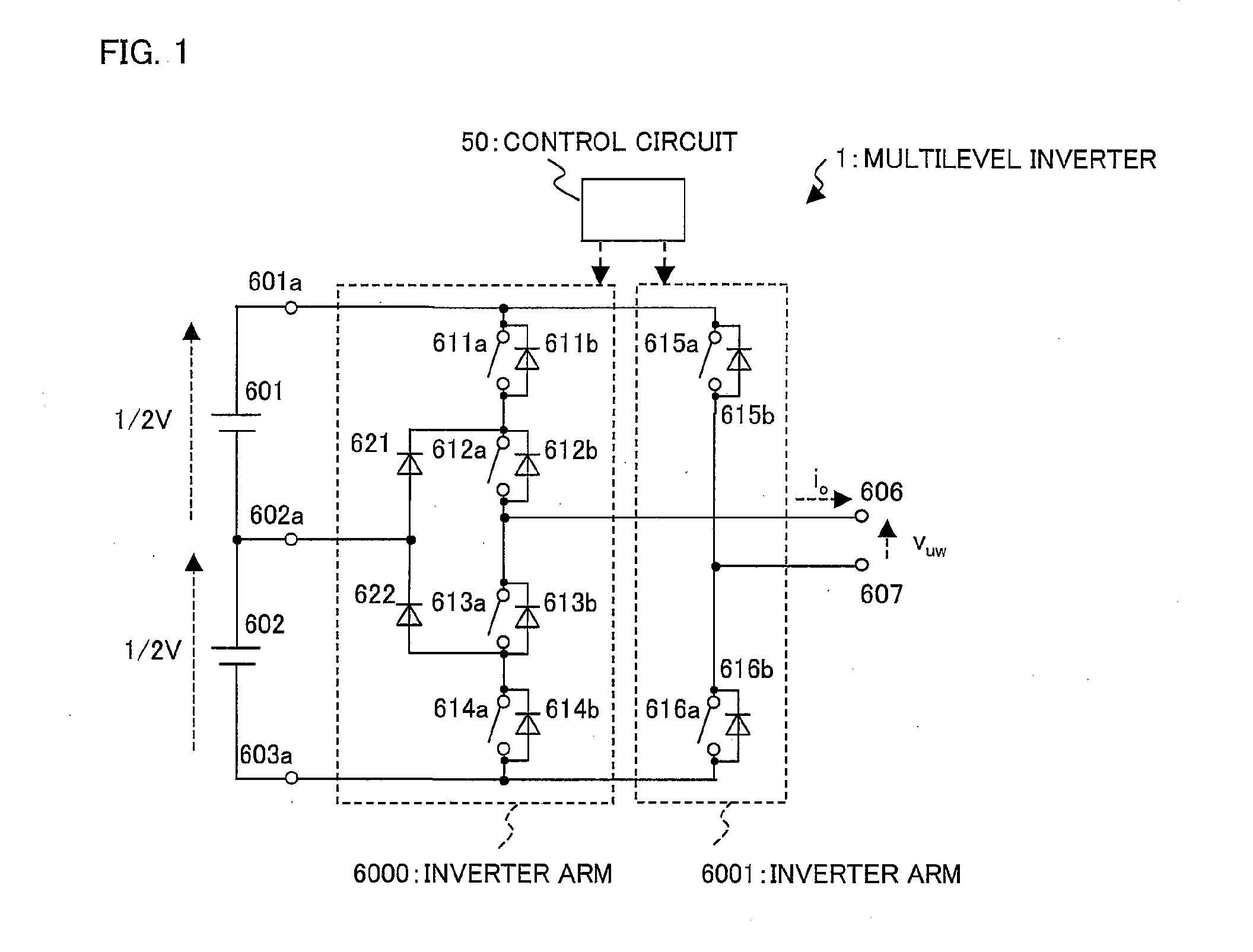
This Nonprovisional application claims priority under 35 U.S.C. §119(a) on Patent Application No. 2010-199961 filed in Japan on Sep. 7, 2010, the entire contents of which are hereby incorporated by reference. The present invention relates to a multilevel inverter. Various multilevel inverters including what is described in Patent Literature 1 have been suggested. Members indicated by reference numerals 101 and 102 are direct current power supplies. The direct current power supply 101 has a positive terminal which is connected to a direct current voltage terminal 101 An inverter arm 131 is provided between the direct current voltage terminals 101 Note that the diodes 111 The single phase three level inverter of ioin The following description specifically discusses Note that The following description discusses how the conventional single phase three level inverter operates. First, during a time period from t1 to t4 in In contrast, the inverter arm 132 of W phase causes the switching element 115 Such switching control causes the state illustrated in Next, during a time period from t4 to t7 in In contrast, the inverter arm 132 of W phase causes the switching element 116 Such switching control causes the state illustrated in The conventional single phase three level inverter of Conventional multilevel inverter-related examples include not only the multilevel inverter of Patent Literature 1 and the conventional single phase three level inverter of Patent Literature 1 Japanese Patent Application Publication, Tokukaihei, No. 5-308778 A (Publication Date: Nov. 19, 1993) Patent Literature 2 Japanese Patent Application Publication, Tokukaihei, No. 11-220886 A (Publication Date: Aug. 10, 1999) Patent Literature 3 Japanese Translation of PCT International Application, Tokuhyosho, No. 63-502953 A (Publication Date: Oct. 27, 1988) The conventional single phase three level inverter of Further, another problem occurs such that it is necessary to provide, as many as gate-source pairs of respective switching elements, floating power supplies for driving the respective switching elements. The present invention has been made in view of the conventional problems, and an object of the present invention is to provide a multilevel inverter in which at least one of (i) the number of switching elements, (ii) the number of diodes, and (iii) the number of floating power supplies has been reduced as compared to a conventional multilevel inverter. In order to attain the object, a multilevel inverter of the present invention includes: a plurality of direct current power supplies which are connected in series; a first output terminal and a second output terminal which output an alternating current voltage; a first inverter arm which supplies, to the first output terminal, either one of (i) a direct current voltage applied to a highest electric potential point in the plurality of direct current power supplies and (ii) a direct current voltage applied to a lowest electric potential point in the plurality of direct current power supplies; and a second inverter arm which supplies, to the second output terminal, any one of (i) the direct current voltage applied to the highest electric potential point, (ii) the direct current voltage applied to the lowest electric potential point, and (iii) a direct current voltage applied to each power supply connection point at which the plurality of direct current power supplies that are adjacent to each other are connected, the first inverter arm including a first switching element group to which two switching elements belong, the two switching elements being (i) connected in series, (ii) provided between the highest electric potential point and the lowest electric potential point, and (iii) connected to respective diodes which are connected in an opposite polarity and in parallel, (i) a connection point at which the two switching elements belonging to the first switching element group are connected and (ii) the first output terminal being connected, the second inverter arm including a second switching element group to which even-numbered switching elements belong, the even-numbered switching elements being (i) connected in series, (ii) provided between the highest electric potential point and the lowest electric potential point, and (iii) connected to respective diodes which are connected in an opposite polarity and in parallel, the second inverter arm further including a first diode and a second diode for the each power supply connection point, the first diode having (i) an anode which is connected to the each power supply connection point and (ii) a cathode which is connected to the highest electric potential point via at least one of the even-numbered switching elements belonging to the second switching element group, the at least one switching element being equal in number to at least one of the plurality of direct current power supplies, the at least one direct current power supply being provided between the highest electric potential point and the each power supply connection point, the second diode having (i) a cathode which is connected to the each power supply connection point and (ii) an anode which is connected to the lowest electric potential point via the other switching elements which belong to the second switching element group and are equal in number to the other direct current power supplies, the other direct current power supplies being provided between the lowest electric potential point and the each power supply connection point, (i) the second output terminal and (ii) one of connection points at which the even-numbered switching elements belonging to the second switching element group are connected to each other being connected, the one connection point being located such that at least one of the even-numbered switching elements provided between the one connection point and the highest electric potential point is equal in number to the other switching elements which belong to the second switching element group and are provided between the one connection point and the lowest electric potential point. According to the invention, in a case where the switching elements of the second inverter arm are suitably controlled to turn on/off, any one of (i) the direct current voltage applied to the highest electric potential point, (ii) the direct current voltage applied to the lowest electric potential point, and (iii) the direct current voltage applied to the each of the power supply connection points can be supplied to the second output terminal. In a case where the switching elements of the first inverter arm are suitably controlled to turn on/off, either one of (i) the direct current voltage applied to the highest electric potential point and (ii) the direct current voltage applied to the lowest electric potential point can be supplied to the first output terminal. This allows the alternating current voltage to be outputted. For example, in a case where a positive output current is outputted via the second output terminal and the second output terminal has its highest electric voltage when a voltage of the first output terminal is a reference voltage, it is only necessary that (i) all the switching elements provided between the highest electric potential point and the second output terminal turn on and (ii) the switching element provided between the lowest electric potential point and the first output terminal turn on. Alternatively, for example, in a case where a negative output current is outputted via the second output terminal and the second output terminal has its highest voltage when a voltage of the first output terminal is a reference voltage, it is only necessary that (i) both the switching elements belonging to the first switching element group turn off and (ii) all the switching elements belonging to the second switching element group turn off. In this case, a current is supplied to each of (i) the diode which is provided between the lowest electric potential point and the first output terminal and connected to a corresponding switching element in an opposite polarity and in parallel and (ii) the diodes which are provided between the highest electric potential point and the second output terminal and connected to respective switching elements in an opposite polarity and in parallel. This allows the negative output current to be outputted via the second output terminal. The first inverter arm has been obtained by simplifying the inverter arm which is provided in the conventional single phase three level inverter described in Background Art and has four switching elements and six diodes. Therefore, two switching elements and four diodes have been reduced in the first inverter arm as compared to the conventional single phase three level inverter. Further, since two switching elements have been reduced as described above, two floating power supplies can be accordingly reduced. This makes it possible to provide a multilevel inverter in which at least one of (i) the number of switching elements, (ii) the number of diodes, and (iii) the number of floating power supplies has been reduced as compared to a conventional multilevel inverter. In order to attain the object, a multilevel inverter of the present invention includes: a plurality of direct current power supplies which are connected in series; a first output terminal and a second output terminal which output an alternating current voltage; a first inverter arm which supplies, to the first output terminal, any one of (i) a direct current voltage applied to a highest electric potential point in the plurality of direct current power supplies, (ii) a direct current voltage applied to a lowest electric potential point in the plurality of direct current power supplies, and (iii) a direct current voltage applied to each power supply connection point at which the plurality of direct current power supplies that are adjacent to each other are connected; and a second inverter arm which supplies, to the second output terminal, any one of (i) the direct current voltage applied to the highest electric potential point, (ii) the direct current voltage applied to the lowest electric potential point, and (iii) the direct current voltage applied to the each power supply connection point, the first inverter arm including a first switching element group to which odd-numbered switching elements belong, the odd-numbered switching elements being (i) connected in series, (ii) provided between the highest electric potential point and the lowest electric potential point, and (iii) connected to respective diodes which are connected in an opposite polarity and in parallel, the first inverter arm further including a first switching element and a first diode for the each power supply connection point, the first switching element having (i) one end which is connected to the each power supply connection point and (ii) the other end which is connected to the highest electric potential point via at least one of the odd-numbered switching elements belonging to the first switching element group, the at least one switching element being equal in number to at least one of the plurality of direct current power supplies, the at least one direct current power supply being provided between the highest electric potential point and the each power supply connection point, the first diode having (i) a cathode which is connected to the each power supply connection point and (ii) an anode which is connected to the lowest electric potential point via the other switching elements which belong to the first switching element group and are equal in number to the other direct current power supplies, the other direct current power supplies being provided between the lowest electric potential point and the each power supply connection point, (i) the first output terminal and (ii) one of connection points at which the odd-numbered switching elements belonging to the first switching element group are connected to each other being connected, the one connection point being located such that at least one of the odd-numbered switching elements provided between the one connection point and the highest electric potential point is smaller in number by one than the other switching elements which belong to the first switching element group and are provided between the one connection point and the lowest electric potential point, the second inverter arm including a second switching element group to which odd-numbered switching elements belong, the odd-numbered switching elements being (i) connected in series, (ii) provided between the highest electric potential point and the lowest electric potential point, and (iii) connected to respective diodes which are connected in an opposite polarity and in parallel, the second inverter arm further including a second switching element and a second diode for the each power supply connection point, the second switching element having (i) one end which is connected to the each power supply connection point and (ii) the other end which is connected to the highest electric potential point via at least one of the odd-numbered switching elements belonging to the second switching element group, the at least one switching element being equal in number to at least one of the plurality of direct current power supplies, the at least one direct current power supply being provided between the highest electric potential point and the each power supply connection point, the second diode having (i) a cathode which is connected to the each power supply connection point and (ii) an anode which is connected to the lowest electric potential point via the other switching elements which belong to the second switching element group and are equal in number to the other direct current power supplies, the other direct current power supplies being provided between the lowest electric potential point and the each power supply connection point, (i) the second output terminal and (ii) one of connection points at which the odd-numbered switching elements belonging to the second switching element group are connected to each other being connected, the one connection point being located such that at least one of the odd-numbered switching elements provided between the one connection point and the highest electric potential point is smaller in number by one than the other switching elements which belong to the second switching element group and are provided between the one connection point and the lowest electric potential point. According to the invention, in a case where the switching elements of the second inverter arm are suitably controlled to turn on/off, any one of (i) the direct current voltage applied to the highest electric potential point, (ii) the direct current voltage applied to the lowest electric potential point, and (iii) the direct current voltage applied to the each of the power supply connection points can be supplied to the second output terminal. In a case where the switching elements of the first inverter arm are suitably controlled to turn on/off, any one of (i) the direct current voltage applied to the highest electric potential point, (ii) the direct current voltage applied to the lowest electric potential point, and (iii) the direct current voltage applied to the each of the power supply connection points can be supplied to the first output terminal. This allows the alternating current voltage to be outputted. For example, in a case where a negative output current is outputted via the second output terminal and the second output terminal has its lowest voltage when a voltage of the first output terminal is a reference voltage, it is only necessary that (i) all the switching elements provided between the highest electric potential point and the first output terminal turn on and (ii) all the switching elements provided between the lowest electric potential point and the second output terminal turn on. Alternatively, for example, in a case where a positive output current is outputted via the second output terminal and the second output terminal has its lowest voltage when a voltage of the first output terminal is a reference voltage, it is only necessary that (i) all the switching elements provided in the second inverter arm turn off and (ii) all the switching elements provided in the first inverter arm turn off. In this case, a current is supplied to each of (i) the diodes which are provided between the lowest electric potential point and the second output terminal and connected to respective switching elements in an opposite polarity and in parallel and (ii) the diodes which are provided between the highest electric potential point and the first output terminal and connected to respective switching elements in an opposite polarity and in parallel. This allows the positive output current to be outputted via the second output terminal. Four diodes have been reduced in the multilevel inverter, especially a three level inverter, as compared to the conventional single phase three level inverter. Though no switching elements have been reduced, sources of respective of (i) the first switching element and the second switching element and (ii) a third switching element which belongs to the first switching element group and one end of which is connected to the highest electric potential point and a fourth switching element which belongs to the second switching element group and one end of which is connected to the highest electric potential point can be shared in a case where (i) and (ii) are MOSFETs. This allows two floating power supply systems to be reduced. This makes it possible to provide a multilevel inverter in which at least one of (i) the number of switching elements, (ii) the number of diodes, and (iii) the number of floating power supplies has been reduced as compared to a conventional multilevel inverter. In order to attain the object, a multilevel inverter of the present invention includes: a plurality of direct current power supplies which are connected in series; a first output terminal and a second output terminal which output an alternating current voltage; a first inverter arm which supplies, to the first output terminal, any one of (i) a direct current voltage applied to a highest electric potential point in the plurality of direct current power supplies, (ii) a direct current voltage applied to a lowest electric potential point in the plurality of direct current power supplies, and (iii) a direct current voltage applied to each power supply connection point at which the plurality of direct current power supplies that are adjacent to each other are connected; and a second inverter arm which supplies, to the second output terminal, any one of (i) the direct current voltage applied to the highest electric potential point, (ii) the direct current voltage applied to the lowest electric potential point, and (iii) the direct current voltage applied to the each power supply connection point, the first inverter arm including a first switching element group to which odd-numbered switching elements belong, the odd-numbered switching elements being (i) connected in series, (ii) provided between the highest electric potential point and the lowest electric potential point, and (iii) connected to respective diodes which are connected in an opposite polarity and in parallel, the first inverter arm further including a first diode and a first switching element for the each power supply connection point, the first diode having (i) an anode which is connected to the each power supply connection point and (ii) a cathode which is connected to the highest electric potential point via at least one of the odd-numbered switching elements belonging to the first switching element group, the at least one switching element being equal in number to at least one of the plurality of direct current power supplies, the at least one direct current power supply being provided between the highest electric potential point and the each power supply connection point, the first switching element having (i) one end which is connected to the each power supply connection point and (ii) the other end which is connected to the lowest electric potential point via the other switching elements which belong to the first switching element group and are equal in number to the other direct current power supplies, the other direct current power supplies being provided between the lowest electric potential point and the each power supply connection point, (i) the first output terminal and (ii) one of connection points at which the odd-numbered switching elements belonging to the first switching element group are connected to each other being connected, the one connection point being located such that at least one of the odd-numbered switching elements provided between the one connection point and the highest electric potential point is larger in number by one than the other switching elements which belong to the first switching element group and are provided between the one connection point and the lowest electric potential point, the second inverter arm including a second switching element group to which odd-numbered switching elements belong, the odd-numbered switching elements being (i) connected in series, (ii) provided between the highest electric potential point and the lowest electric potential point, and (iii) connected to respective diodes which are connected in an opposite polarity and in parallel, the second inverter arm further including a second diode and a second switching element for the each power supply connection point, the second diode having (i) an anode which is connected to the each power supply connection point and (ii) a cathode which is connected to the highest electric potential point via at least one of the odd-numbered switching elements belonging to the second switching element group, the at least one switching element being equal in number to at least one of the plurality of direct current power supplies, the at least one direct current power supply being provided between the highest electric potential point and the each power supply connection point, the second switching element having (i) one end which is connected to the each power supply connection point and (ii) the other end which is connected to the lowest electric potential point via the other switching elements which belong to the second switching element group and are equal in number to the other direct current power supplies, the other direct current power supplies being provided between the lowest electric potential point and the each power supply connection point, (i) the second output terminal and (ii) one of connection points at which the odd-numbered switching elements belonging to the second switching element group are connected to each other being connected, the one connection point being located such that at least one of the odd-numbered switching elements provided between the one connection point and the highest electric potential point is larger in number by one than the other switching elements which belong to the second switching element group and are provided between the one connection point and the lowest electric potential point. According to the invention, in a case where the switching elements of the second inverter arm are suitably controlled to turn on/off, any one of (i) the direct current voltage applied to the highest electric potential point, (ii) the direct current voltage applied to the lowest electric potential point, and (iii) the direct current voltage applied to the each of the power supply connection points can be supplied to the second output terminal. In a case where the switching elements of the first inverter arm are suitably controlled to turn on/off, any one of (i) the direct current voltage applied to the highest electric potential point, (ii) the direct current voltage applied to the lowest electric potential point, and (iii) the direct current voltage applied to the each of the power supply connection points can be supplied to the first output terminal. This allows the alternating current voltage to be outputted. For example, in a case where a negative output current is outputted via the second output terminal and the second output terminal has its lowest voltage when a voltage of the first output terminal is a reference voltage, it is only necessary that (i) all the switching elements provided between the highest electric potential point and the first output terminal turn on and (ii) all the switching elements provided between the lowest electric potential point and the second output terminal turn on. Alternatively, for example, in a case where a negative output current is outputted via the second output terminal and the second output terminal has its highest voltage when a voltage of the first output terminal is a reference voltage, it is only necessary that (i) all the switching elements provided in the first inverter arm turn off and (ii) all the switching elements provided in the second inverter arm turn off. In this case, a current is supplied to each of (i) the diodes which are provided between the lowest electric potential point and the first output terminal and connected to respective switching elements in an opposite polarity and in parallel and (ii) the diodes which are provided between the highest electric potential point and the second output terminal and connected to respective switching elements in an opposite polarity and in parallel. This allows the negative output current to be outputted via the second output terminal. Four diodes have been reduced in the multilevel inverter, especially a three level inverter, as compared to the conventional single phase three level inverter. This makes it possible to provide a multilevel inverter in which at least one of (i) the number of switching elements, (ii) the number of diodes, and (iii) the number of floating power supplies has been reduced as compared to a conventional multilevel inverter. As described earlier, the multilevel inverter of the present invention is arranged to include the first inverter arm including a first switching element group to which two switching elements belong, the two switching elements being (i) connected in series, (ii) provided between the highest electric potential point and the lowest electric potential point, and (iii) connected to respective diodes which are connected in an opposite polarity and in parallel, (i) a connection point at which the two switching elements belonging to the first switching element group are connected and (ii) the first output terminal being connected, the second inverter arm including a second switching element group to which even-numbered switching elements belong, the even-numbered switching elements being (i) connected in series, (ii) provided between the highest electric potential point and the lowest electric potential point, and (iii) connected to respective diodes which are connected in an opposite polarity and in parallel, the second inverter arm further including a first diode and a second diode for the each power supply connection point, the first diode having (i) an anode which is connected to the each power supply connection point and (ii) a cathode which is connected to the highest electric potential point via at least one of the even-numbered switching elements belonging to the second switching element group, the at least one switching element being equal in number to at least one of the plurality of direct current power supplies, the at least one direct current power supply being provided between the highest electric potential point and the each power supply connection point, the second diode having (i) a cathode which is connected to the each power supply connection point and (ii) an anode which is connected to the lowest electric potential point via the other switching elements which belong to the second switching element group and are equal in number to the other direct current power supplies, the other direct current power supplies being provided between the lowest electric potential point and the each power supply connection point, (i) the second output terminal and (ii) one of connection points at which the even-numbered switching elements belonging to the second switching element group are connected to each other being connected, the one connection point being located such that at least one of the even-numbered switching elements provided between the one connection point and the highest electric potential point is equal in number to the other switching elements which belong to the second switching element group and are provided between the one connection point and the lowest electric potential point. As described earlier, the multilevel inverter of the present invention is arranged to include the first inverter arm including a first switching element group to which odd-numbered switching elements belong, the odd-numbered switching elements being (i) connected in series, (ii) provided between the highest electric potential point and the lowest electric potential point, and (iii) connected to respective diodes which are connected in an opposite polarity and in parallel, the first inverter arm further including a first switching element and a first diode for the each power supply connection point, the first switching element having (i) one end which is connected to the each power supply connection point and (ii) the other end which is connected to the highest electric potential point via at least one of the odd-numbered switching elements belonging to the first switching element group, the at least one switching element being equal in number to at least one of the plurality of direct current power supplies, the at least one direct current power supply being provided between the highest electric potential point and the each power supply connection point, the first diode having (i) a cathode which is connected to the each power supply connection point and (ii) an anode which is connected to the lowest electric potential point via the other switching elements which belong to the first switching element group and are equal in number to the other direct current power supplies, the other direct current power supplies being provided between the lowest electric potential point and the each power supply connection point, (i) the first output terminal and (ii) one of connection points at which the odd-numbered switching elements belonging to the first switching element group are connected to each other being connected, the one connection point being located such that at least one of the odd-numbered switching elements provided between the one connection point and the highest electric potential point is smaller in number by one than the other switching elements which belong to the first switching element group and are provided between the one connection point and the lowest electric potential point, the second inverter arm including a second switching element group to which odd-numbered switching elements belong, the odd-numbered switching elements being (i) connected in series, (ii) provided between the highest electric potential point and the lowest electric potential point, and (iii) connected to respective diodes which are connected in an opposite polarity and in parallel, the second inverter arm further including a second switching element and a second diode for the each power supply connection point, the second switching element having (i) one end which is connected to the each power supply connection point and (ii) the other end which is connected to the highest electric potential point via at least one of the odd-numbered switching elements belonging to the second switching element group, the at least one switching element being equal in number to at least one of the plurality of direct current power supplies, the at least one direct current power supply being provided between the highest electric potential point and the each power supply connection point, the second diode having (i) a cathode which is connected to the each power supply connection point and (ii) an anode which is connected to the lowest electric potential point via the other switching elements which belong to the second switching element group and are equal in number to the other direct current power supplies, the other direct current power supplies being provided between the lowest electric potential point and the each power supply connection point, (i) the second output terminal and (ii) one of connection points at which the odd-numbered switching elements belonging to the second switching element group are connected to each other being connected, the one connection point being located such that at least one of the odd-numbered switching elements provided between the one connection point and the highest electric potential point is smaller in number by one than the other switching elements which belong to the second switching element group and are provided between the one connection point and the lowest electric potential point. As described earlier, the multilevel inverter of the present invention is arranged to include the first inverter arm including a first switching element group to which odd-numbered switching elements belong, the odd-numbered switching elements being (i) connected in series, (ii) provided between the highest electric potential point and the lowest electric potential point, and (iii) connected to respective diodes which are connected in an opposite polarity and in parallel, the first inverter arm further including a first diode and a first switching element for the each power supply connection point, the first diode having (i) an anode which is connected to the each power supply connection point and (ii) a cathode which is connected to the highest electric potential point via at least one of the odd-numbered switching elements belonging to the first switching element group, the at least one switching element being equal in number to at least one of the plurality of direct current power supplies, the at least one direct current power supply being provided between the highest electric potential point and the each power supply connection point, the first switching element having (i) one end which is connected to the each power supply connection point and (ii) the other end which is connected to the lowest electric potential point via the other switching elements which belong to the first switching element group and are equal in number to the other direct current power supplies, the other direct current power supplies being provided between the lowest electric potential point and the each power supply connection point, (i) the first output terminal and (ii) one of connection points at which the odd-numbered switching elements belonging to the first switching element group are connected to each other being connected, the one connection point being located such that at least one of the odd-numbered switching elements provided between the one connection point and the highest electric potential point is larger in number by one than the other switching elements which belong to the first switching element group and are provided between the one connection point and the lowest electric potential point, the second inverter arm including a second switching element group to which odd-numbered switching elements belong, the odd-numbered switching elements being (i) connected in series, (ii) provided between the highest electric potential point and the lowest electric potential point, and (iii) connected to respective diodes which are connected in an opposite polarity and in parallel, the second inverter arm further including a second diode and a second switching element for the each power supply connection point, the second diode having (i) an anode which is connected to the each power supply connection point and (ii) a cathode which is connected to the highest electric potential point via at least one of the odd-numbered switching elements belonging to the second switching element group, the at least one switching element being equal in number to at least one of the plurality of direct current power supplies, the at least one direct current power supply being provided between the highest electric potential point and the each power supply connection point, the second switching element having (i) one end which is connected to the each power supply connection point and (ii) the other end which is connected to the lowest electric potential point via the other switching elements which belong to the second switching element group and are equal in number to the other direct current power supplies, the other direct current power supplies being provided between the lowest electric potential point and the each power supply connection point, (i) the second output terminal and (ii) one of connection points at which the odd-numbered switching elements belonging to the second switching element group are connected to each other being connected, the one connection point being located such that at least one of the odd-numbered switching elements provided between the one connection point and the highest electric potential point is larger in number by one than the other switching elements which belong to the second switching element group and are provided between the one connection point and the lowest electric potential point. This brings about an effect of providing a multilevel inverter in which at least one of (i) the number of switching elements, (ii) the number of diodes, and (iii) the number of floating power supplies has been reduced as compared to a conventional multilevel inverter. Embodiments of the present invention are described below with reference to The multilevel inverter 1 of The multilevel inverter 1 generally includes direct current power supplies 601 and 602 (a plurality of direct power supplies), an inverter arm 6000 (a second inverter arm), and an inverter arm 6001 (a first inverter arm). The direct current power supply 601 has a positive terminal which is connected to a direct current voltage terminal 601 The inverter arm 6000 is provided between the direct current voltage terminals 601 The inverter arm 6001 is provided between the direct current voltage terminals 601 In the multilevel inverter 1 of The other end of the switching element 611 The other end of the switching element 612 The other end of the switching element 615 The other end of the switching element 613 An anode of the diode 621, a cathode of the diode 622, and the direct current voltage terminal 602 The other end of the switching element 614 Note that a state in which a switching element and a diode are connected in an opposite polarity and in parallel refers to the following state: Assume that one end of a switch and a cathode of a diode are connected, and the other end of the switch and an anode of the diode are connected. Even in a case the switch turns on and a current flows from one end to the other end of the switch, the diode does not turn on. The inverter arm 6001 of the multilevel inverter 1 of This makes it possible to provide a multilevel (single phase three level) inverter in which at least one of (i) the number of switching elements, (ii) the number of diodes, and (iii) the number of floating power supplies has been reduced as compared to the conventional single phase three level inverter of (Load in Which Line Voltage vuwand Output Current ioare in Phase with Each Other) Note that a utility interactive inverter is connected to a commercial system, which serves as a load, so as to supply alternating current power. The following description specifically discusses First, during the time periods (i) from t1 to t2 and (ii) from t3 to t4 in U phase carries out PWM control with respect to the switching elements 612 In contrast, the inverter arm 6001 of W phase causes the switching element 615 Such switching control causes the state illustrated in Next, during the time period from t2 to t3 in In contrast, the inverter arm 6001 of W phase causes the switching element 615 Such switching control causes the state illustrated in Subsequently, during the time periods (i) from t4 to t5 and (ii) from t6 to t7 in In contrast, the inverter arm 6001 of W phase causes the switching element 615 Such switching control causes the state illustrated in Then, during the time period from t5 to t6 in In contrast, the inverter arm 6001 of W phase causes the switching element 615 Such switching control causes the state illustrated in The multilevel inverter 1 of (Load in Which Line Voltage vuwand Output Current ioHave Different Phases) How the utility interactive inverter operates is described here. The utility interactive inverter basically carries out two operations, i.e., an interactive operation and an autonomous operation. The interactive operation is an operation in which the utility interactive inverter is connected to a commercial system, so as to supply alternating current power. In contrast, the autonomous operation is an operation in which the utility interactive inverter is connected to no commercial system, so as to supply alternating current power to various loads that are not commercial systems. A state in which each of the various loads, to which the utility interactive inverter is connected during the autonomous operation, is the L load such as a motor is to be referred to as the “L load in which the utility interactive inverter autonomously operates” as described earlier. The following description specifically discusses First, in the case where the output current iois positive during the time periods (i) from t1 to t2 and (ii) from t3 to t4 in In contrast, in the case where the output current iois negative during the time periods (i) from t1 to t2 and (ii) from t3 to t4 in Such switching control causes the state illustrated in Next, in the case where the output current iois positive during the time period from t2 to t3 in In contrast, in the case where the output current iois negative during the time period from t2 to t3 in Such switching control causes the state illustrated in Subsequently, in the case where the output current iois negative during the time periods (i) from t4 to t5 and (ii) from t6 to t7 in In contrast, in the case where the output current iois positive during the time periods (i) from t4 to t5 and (ii) from t6 to t7 in Such switching control causes the state illustrated in Then, in the case where the output current iois negative during the time period from t5 to t6 in In contrast, in the case where the output current iois positive during the time period from t5 to t6 in Such switching control causes the state illustrated in The multilevel inverter 1 of As described earlier, according to the multilevel inverter 1 in accordance with the first embodiment of the present invention, the switching elements of the inverter arm 6000 are suitably controlled to turn on/off. This allows any one of (i) a direct current voltage applied to the highest electric potential point, (ii) a direct current voltage applied to the lowest electric potential point, and (iii) a direct current voltage applied to the power supply connection point to be supplied to the U phase output terminal 606. In a case where the switching elements of the inverter arm 6001 are suitably controlled to turn on/off, either one of (i) the direct current voltage applied to the highest electric potential point and (ii) the direct current voltage applied to the lowest electric potential point can be supplied to the W phase output terminal 607. This allows the line voltage vuwto be outputted. The multilevel inverter 1 further includes a control circuit 50 (control means). The control circuit 50 can supply signals to the respective switching elements 615 This allows a voltage which has been subjected to PWM control to be outputted as the line voltage vuw. Further, the multilevel inverter 1 is usable both for a load which requires the output current ioto be positive and for a load which requires the output current ioto be negative. Note that an inverter arm 6000′ of Patent Literature 2 illustrated in A second embodiment of the present invention is described below with reference to The multilevel inverter 2 of The multilevel inverter 2 generally includes direct current power supplies 901 and 902 (a plurality of direct power supplies), an inverter arm 9000 (a second inverter arm), and an inverter arm 9001 (a first inverter arm). The direct current power supply 901 has a positive terminal which is connected to a direct current voltage terminal 901 The inverter arm 9000 is provided between the direct current voltage terminals 901 The inverter arm 9001 is provided between the direct current voltage terminals 901 In the multilevel inverter 2 of The other end of the switching element 911 The other end of the switching element 912 The other end of the switching element 914 The other end of the switching element 915 One end of the switching element 931, a cathode of the diode 921, one end of the switching element 932, a cathode of the diode 922, and the direct current voltage terminal 902 The other end of the switching element 913 Four diodes have been reduced in the multilevel inverter 2 of This makes it possible to provide a multilevel (single phase three level) inverter in which at least one of (i) the number of switching elements, (ii) the number of diodes, and (iii) the number of floating power supplies has been reduced as compared to the conventional single phase three level inverter of The following description specifically discusses First, in the case where the output current iois positive during the time periods (i) from t 1 to t2 and (ii) from t3 to t4 in Such switching control causes the state illustrated in In contrast, in the case where the output current iois negative during the time periods (i) from t1 to t2 and (ii) from t3 to t4 in Such switching control causes the state illustrated in Next, in the case where the output current iois positive during the time period from t2 to t3 in Such switching control causes the state illustrated in In contrast, in the case where the output current iois negative during the time period from t2 to t3 in Such switching control causes the state illustrated in Subsequently, in the case where the output current iois negative during the time periods (i) from t4 to t5 and (ii) from t6 to t7 in Such switching control causes the state illustrated in In contrast, in the case where the output current iois positive during the time periods (i) from t4 to t5 and (ii) from t6 to t7 in Such switching control causes the state illustrated in Then, in the case where the output current iois negative during the time period from t5 to t6 in Such switching control causes the state illustrated in In contrast, in the case where the output current iois positive during the time period from t5 to t6 in Such switching control causes the state illustrated in The multilevel inverter 2 of As described earlier, according to the multilevel inverter 2 in accordance with the second embodiment of the present invention, the switching elements of the inverter arm 9000 are suitably controlled to turn on/off. This allows any one of (i) a direct current voltage applied to the highest electric potential point, (ii) a direct current voltage applied to the lowest electric potential point, and (iii) a direct current voltage applied to the power supply connection point to be supplied to the U phase output terminal 906. The switching elements of the inverter arm 9001 are also suitably controlled to turn on/off. This allows any one of (i) the direct current voltage applied to the highest electric potential point, (ii) the direct current voltage applied to the lowest electric potential point, and (iii) the direct current voltage applied to the power supply connection point to be supplied to the W phase output terminal 907. This allows the line voltage vuwto be outputted. The multilevel inverter 2 can further include a control circuit 50 (control means). The control circuit supplies signals to the respective switching elements 914 This allows a voltage which has been subjected to PWM control to be outputted as the line voltage vuw. Further, the multilevel inverter 2 is usable both for a load which requires the output current ioto be positive and for a load which requires the output current ioto be negative. A multilevel inverter 2′ of In the multilevel inverter 2′ of The multilevel inverter 2′ in accordance with the modification includes direct current power supplies 901 and 902 which are connected in series, and a U phase output terminal 906 and a W phase output terminal 907 which output a line voltage vuw. The multilevel inverter 2′ further includes the inverter arm 9001′ which supplies, to the W phase output terminal 907, any one of (i) a direct current voltage applied to a highest electric potential point 901 According to the arrangement, the switching elements of the inverter arm 9000′ can be suitably controlled to turn on/off. This allows any one of (i) the direct current voltage applied to the highest electric potential point 901 For example, assume that a negative output current iois outputted via the U phase output terminal 906 and the U phase output terminal 906 has a voltage (the line voltage vuw) of −V when a voltage of the W phase output terminal 907 is a reference voltage. In this case, it is only necessary that (i) both the switching elements 915 Alternatively, for example, assume that the negative output current iois outputted via the U phase output terminal 906 and the U phase output terminal 906 has the voltage (the line voltage vuw) of V when a voltage of the W phase output terminal 907 is a reference voltage. In this case, it is only necessary that (i) the switching element 914 In the multilevel inverter 2′, four diodes have been reduced as compared to the conventional single phase three level inverter of This makes it possible to provide a multilevel (single phase three level) inverter in which at least one of (i) the number of switching elements, (ii) the number of diodes, and (iii) the number of floating power supplies has been reduced as compared to the conventional single phase three level inverter. A three phase three level inverter 2″ can be arranged as an extended modification of the second embodiment by adding, to the multilevel inverter 2 of Note that the inverter arms 9000 and 9001 have an identical configuration according to the multilevel inverter 2 and the inverter arms 9000′ and 9001′ have an identical arrangement according to the multilevel inverter 2′. Note here that a multilevel inverter cannot be arranged by, for example, combining the inverter arms 9000 and 9001′. This is because of the following reason. In a case where an output voltage vuwis positive and a multilevel output is produced in one of the inverter arms 9000 and 9001′, an output voltage vuwis negative and a two level output is produced in the other of the inverter arms 9000 and 9001′. In contrast, in a case where an output voltage vuwis negative and a multilevel output is produced in one of the inverter arms 9000 and 9001′, an output voltage vuwis positive and a two level output is produced in the other of the inverter arms 9000 and 9001′. [Switching Element] A semiconductor switch is usable as each of the switching elements of the first and second embodiments. Each of the multilevel inverters 1, 2, and 2′ can be arranged by use of the semiconductor switch but without using a mechanical switch. However, for example, a semiconductor switch such as a MOSFET (metal-oxide-semiconductor field-effect transistor) having a parasitic antiparallel diode is not usable as each of the switching elements 931 and 932 of In contrast, a semiconductor switch such as a MOSFET (described above) having a parasitic antiparallel diode is usable as each of (i) the switching elements 611 In a case where a MOSFET is used as a switching element, it is only necessary that a MOSFET having a polarity illustrated in In a case where an IGBT (Insulated Gate Bipolar Transistor) is used as a switching element, it is only necessary that an IGBT having a polarity illustrated in [Number of Levels of Multilevel Inverter] The embodiments of the present invention discussed a three level inverter. However, the present invention is not limited to this, and is applicable to a multilevel inverter of various levels of four level, five level, . . . . For example, Note that the embodiments of the present invention mainly discussed a utility interactive inverter. However, the present invention is applicable not only to a utility interactive inverter but also to an inverter for a motor drive. The multilevel inverter can be arranged to further include control means for supplying signals to the respective switching elements belong to the first and second switching element groups, the signals controlling the respective switching elements belong to the first and second switching element groups. The control means can carry out switching control so as to prevent (i) all the switching elements belonging to the first switching element group from simultaneously turning on and (ii) all the switching elements belonging to the second switching element group from simultaneously turning on. In addition to such switching control, of the switching elements belonging to the second switching element group, the control means can (i) carry out PWM control with respect to any given number of switching elements and (ii) control the other switching elements to keep turning on/off. The control means can further control any one of the switching elements belonging to the first switching element group to turn on/off in accordance with a polarity of an output current outputted via the second output terminal. This allows a voltage which has been subjected to PWM control to be outputted as the alternating current voltage. Further, the multilevel inverter is usable both for a load which requires the output current to be positive and for a load which requires the output current to be negative. According to the multilevel inverter, each of (i) the switching elements belonging to the first switching element group and (ii) the switching elements belonging to the second switching element group can be a semiconductor switch. According to this, the multilevel inverter can be arranged without using a mechanical switch. Any one of the multilevel inverters can further include control means. The control means supplies signals to the respective switching elements, the signals controlling the respective switching elements. The control means can control (i) the switching elements belonging to the first switching element group, (ii) the switching elements belonging to the second switching element group, (iii) the first switching element, and (iv) the second switching element. The control means can carry out switching control so as to prevent (i) all the switching elements belonging to the first switching element group from simultaneously turning on and (ii) all the switching elements belonging to the second switching element group from simultaneously turning on. In addition to such switching control, the control means can carry out PWM control with respect to either one of (i) any given number of switching elements of the switching elements provided between the lowest electric potential point or the highest electric potential point and the first output terminal and (ii) any given number of switching elements of the switching elements provided between the lowest electric potential point or the highest electric potential point and the second output terminal. The control means can control a switching element of the other switching elements which is provided between the highest electric potential point or the lowest electric potential point and each of the first and second output terminals to keep turning on/off. The control means can further control each of (i) the switching elements provided between the highest electric potential point or the lowest electric potential point and the first output terminal, (ii) the switching elements provided between the highest electric potential point or the lowest electric potential point and the second output terminal, (iii) the first switching element, and (iv) the second switching element to turn on/off in accordance with a polarity of the output current outputted via the second output terminal. This allows a voltage which has been subjected to PWM control to be outputted as the alternating current voltage. Further, the multilevel inverter is usable both for a load which requires the output current to be positive and for a load which requires the output current to be negative. According to any one of the multilevel inverters, each of (i) the switching elements belonging to the first switching element group, (ii) the switching elements belonging to the second switching element group, (iii) the first switching element, and (iv) the second switching element can be a semiconductor switch. According to this, the multilevel inverter can be arranged without using a mechanical switch. The present invention is not limited to the description of the embodiments above, but may be altered by a skilled person within the scope of the claims. An embodiment based on a proper combination of technical means disclosed in different embodiments is encompassed in the technical scope of the present invention. Since a multilevel inverter of the present invention allows a reduction in at least one of (i) the number of switching elements, (ii) the number of diodes, and (iii) the number of floating power supplies has been reduced as compared to a conventional multilevel inverter, the present invention is suitably usable for a multilevel inverter which is required to have a smaller circuit and to be made at a lower cost. 1, 2, 2′ Multilevel Inverter 2″ Three phase three level inverter 6000 Inverter arm (Second inverter arm) 6001 Inverter arm (First inverter arm) 6000′ Inverter arm 601, 602 Direct current power supply (A plurality of direct current power supplies) 601 606 U phase output terminal (Second output terminal) 607 W phase output terminal (First output terminal) 611 615 611 615 621 Diode 622 Diode 9000, 9000′ Inverter arm (Second inverter arm) 9001, 9001′ Inverter arm (First inverter arm) 9002 Inverter arm 901, 902 Direct current power supply (A plurality of direct current power supplies) 901 906 U phase output terminal (Second output terminal) 907 W phase output terminal (First output terminal) 911 911 914 914 931, 931′ Switching element (Second switching element) 932, 932′ Switching element (First switching element) 911 911 914 914 921, 921′ Diode 922, 922′ Diode 50 Control circuit (Control means) ioOutput current vuwLine voltage (Alternating current voltage) A multilevel inverter includes an inverter arm. The inverter arm is provided between a highest electric potential point and a lowest electric potential point, and includes (i) a second switching element group to which switching elements that are connected in series belong, the switching elements being connected to respective diodes which are connected in an opposite polarity and in parallel and (ii) a diode for each power supply connection point. One of connection points at which the switching elements belonging to the second switching element group are connected to each other and a U phase output terminal are connected, the one connection point being located such that at least one of the switching elements provided between the one connection point and the highest electric potential point is equal in number to the other switching elements which belong to the second switching element group and are provided between the one connection point and the lowest electric potential point. 1. A multilevel inverter comprising:
a plurality of direct current power supplies which are connected in series; a first output terminal and a second output terminal which output an alternating current voltage; a first inverter arm which supplies, to the first output terminal, either one of (i) a direct current voltage applied to a highest electric potential point in the plurality of direct current power supplies and (ii) a direct current voltage applied to a lowest electric potential point in the plurality of direct current power supplies; and a second inverter arm which supplies, to the second output terminal, any one of (i) the direct current voltage applied to the highest electric potential point, (ii) the direct current voltage applied to the lowest electric potential point, and (iii) a direct current voltage applied to each power supply connection point at which the plurality of direct current power supplies that are adjacent to each other are connected, the first inverter arm including a first switching element group to which two switching elements belong, the two switching elements being (i) connected in series, (ii) provided between the highest electric potential point and the lowest electric potential point, and (iii) connected to respective diodes which are connected in an opposite polarity and in parallel, (i) a connection point at which the two switching elements belonging to the first switching element group are connected and (ii) the first output terminal being connected, the second inverter arm including a second switching element group to which even-numbered switching elements belong, the even-numbered switching elements being (i) connected in series, (ii) provided between the highest electric potential point and the lowest electric potential point, and (iii) connected to respective diodes which are connected in an opposite polarity and in parallel, the second inverter arm further including a first diode and a second diode for the each power supply connection point, the first diode having (i) an anode which is connected to the each power supply connection point and (ii) a cathode which is connected to the highest electric potential point via at least one of the even-numbered switching elements belonging to the second switching element group, the at least one switching element being equal in number to at least one of the plurality of direct current power supplies, the at least one direct current power supply being provided between the highest electric potential point and the each power supply connection point, the second diode having (i) a cathode which is connected to the each power supply connection point and (ii) an anode which is connected to the lowest electric potential point via the other switching elements which belong to the second switching element group and are equal in number to the other direct current power supplies, the other direct current power supplies being provided between the lowest electric potential point and the each power supply connection point, (i) the second output terminal and (ii) one of connection points at which the even-numbered switching elements belonging to the second switching element group are connected to each other being connected, the one connection point being located such that at least one of the even-numbered switching elements provided between the one connection point and the highest electric potential point is equal in number to the other switching elements which belong to the second switching element group and are provided between the one connection point and the lowest electric potential point. 2. A multilevel inverter comprising:
a plurality of direct current power supplies which are connected in series; a first output terminal and a second output terminal which output an alternating current voltage; a first inverter arm which supplies, to the first output terminal, any one of (i) a direct current voltage applied to a highest electric potential point in the plurality of direct current power supplies, (ii) a direct current voltage applied to a lowest electric potential point in the plurality of direct current power supplies, and (iii) a direct current voltage applied to each power supply connection point at which the plurality of direct current power supplies that are adjacent to each other are connected; and a second inverter arm which supplies, to the second output terminal, any one of (i) the direct current voltage applied to the highest electric potential point, (ii) the direct current voltage applied to the lowest electric potential point, and (iii) the direct current voltage applied to the each power supply connection point, the first inverter arm including a first switching element group to which odd-numbered switching elements belong, the odd-numbered switching elements being (i) connected in series, (ii) provided between the highest electric potential point and the lowest electric potential point, and (iii) connected to respective diodes which are connected in an opposite polarity and in parallel, the first inverter arm further including a first switching element and a first diode for the each power supply connection point, the first switching element having (i) one end which is connected to the each power supply connection point and (ii) the other end which is connected to the highest electric potential point via at least one of the odd-numbered switching elements belonging to the first switching element group, the at least one switching element being equal in number to at least one of the plurality of direct current power supplies, the at least one direct current power supply being provided between the highest electric potential point and the each power supply connection point, the first diode having (i) a cathode which is connected to the each power supply connection point and (ii) an anode which is connected to the lowest electric potential point via the other switching elements which belong to the first switching element group and are equal in number to the other direct current power supplies, the other direct current power supplies being provided between the lowest electric potential point and the each power supply connection point, (i) the first output terminal and (ii) one of connection points at which the odd-numbered switching elements belonging to the first switching element group are connected to each other being connected, the one connection point being located such that at least one of the odd-numbered switching elements provided between the one connection point and the highest electric potential point is smaller in number by one than the other switching elements which belong to the first switching element group and are provided between the one connection point and the lowest electric potential point, the second inverter arm including a second switching element group to which odd-numbered switching elements belong, the odd-numbered switching elements being (i) connected in series, (ii) provided between the highest electric potential point and the lowest electric potential point, and (iii) connected to respective diodes which are connected in an opposite polarity and in parallel, the second inverter arm further including a second switching element and a second diode for the each power supply connection point, the second switching element having (i) one end which is connected to the each power supply connection point and (ii) the other end which is connected to the highest electric potential point via at least one of the odd-numbered switching elements belonging to the second switching element group, the at least one switching element being equal in number to at least one of the plurality of direct current power supplies, the at least one direct current power supply being provided between the highest electric potential point and the each power supply connection point, the second diode having (i) a cathode which is connected to the each power supply connection point and (ii) an anode which is connected to the lowest electric potential point via the other switching elements which belong to the second switching element group and are equal in number to the other direct current power supplies, the other direct current power supplies being provided between the lowest electric potential point and the each power supply connection point, (i) the second output terminal and (ii) one of connection points at which the odd-numbered switching elements belonging to the second switching element group are connected to each other being connected, the one connection point being located such that at least one of the odd-numbered switching elements provided between the one connection point and the highest electric potential point is smaller in number by one than the other switching elements which belong to the second switching element group and are provided between the one connection point and the lowest electric potential point. 3. A multilevel inverter comprising:
a plurality of direct current power supplies which are connected in series; a first output terminal and a second output terminal which output an alternating current voltage; a first inverter arm which supplies, to the first output terminal, any one of (i) a direct current voltage applied to a highest electric potential point in the plurality of direct current power supplies, (ii) a direct current voltage applied to a lowest electric potential point in the plurality of direct current power supplies, and (iii) a direct current voltage applied to each power supply connection point at which the plurality of direct current power supplies that are adjacent to each other are connected; and a second inverter arm which supplies, to the second output terminal, any one of (i) the direct current voltage applied to the highest electric potential point, (ii) the direct current voltage applied to the lowest electric potential point, and (iii) the direct current voltage applied to the each power supply connection point, the first inverter arm including a first switching element group to which odd-numbered switching elements belong, the odd-numbered switching elements being (i) connected in series, (ii) provided between the highest electric potential point and the lowest electric potential point, and (iii) connected to respective diodes which are connected in an opposite polarity and in parallel, the first inverter arm further including a first diode and a first switching element for the each power supply connection point, the first diode having (i) an anode which is connected to the each power supply connection point and (ii) a cathode which is connected to the highest electric potential point via at least one of the odd-numbered switching elements belonging to the first switching element group, the at least one switching element being equal in number to at least one of the plurality of direct current power supplies, the at least one direct current power supply being provided between the highest electric potential point and the each power supply connection point, the first switching element having (i) one end which is connected to the each power supply connection point and (ii) the other end which is connected to the lowest electric potential point via the other switching elements which belong to the first switching element group and are equal in number to the other direct current power supplies, the other direct current power supplies being provided between the lowest electric potential point and the each power supply connection point, (i) the first output terminal and (ii) one of connection points at which the odd-numbered switching elements belonging to the first switching element group are connected to each other being connected, the one connection point being located such that at least one of the odd-numbered switching elements provided between the one connection point and the highest electric potential point is larger in number by one than the other switching elements which belong to the first switching element group and are provided between the one connection point and the lowest electric potential point, the second inverter arm including a second switching element group to which odd-numbered switching elements belong, the odd-numbered switching elements being (i) connected in series, (ii) provided between the highest electric potential point and the lowest electric potential point, and (iii) connected to respective diodes which are connected in an opposite polarity and in parallel, the second inverter arm further including a second diode and a second switching element for the each power supply connection point, the second diode having (i) an anode which is connected to the each power supply connection point and (ii) a cathode which is connected to the highest electric potential point via at least one of the odd-numbered switching elements belonging to the second switching element group, the at least one switching element being equal in number to at least one of the plurality of direct current power supplies, the at least one direct current power supply being provided between the highest electric potential point and the each power supply connection point, the second switching element having (i) one end which is connected to the each power supply connection point and (ii) the other end which is connected to the lowest electric potential point via the other switching elements which belong to the second switching element group and are equal in number to the other direct current power supplies, the other direct current power supplies being provided between the lowest electric potential point and the each power supply connection point, (i) the second output terminal and (ii) one of connection points at which the odd-numbered switching elements belonging to the second switching element group are connected to each other being connected, the one connection point being located such that at least one of the odd-numbered switching elements provided between the one connection point and the highest electric potential point is larger in number by one than the other switching elements which belong to the second switching element group and are provided between the one connection point and the lowest electric potential point. 4. The multilevel inverter as set forth in the control means carrying out switching control so that: (i) both the two switching elements belonging to the first switching element group are prevented from simultaneously turning on; (ii) all the even-numbered switching elements belonging to the second switching element group are prevented from simultaneously turning on; (iii) of the even-numbered switching elements belonging to the second switching element group, any given number of switching elements is subjected to pulse width modulation control and the other switching elements are kept turning on/off; and (iv) either one of the two switching elements belonging to the first switching element group turns on/off in accordance with a polarity of an output current outputted via the second output terminal. 5. The multilevel inverter as set forth in the control means carrying out switching control so that: (i) all the odd-numbered switching elements belonging to the first switching element group are prevented from simultaneously turning on; (ii) all the odd-numbered switching elements belonging to the second switching element group are prevented from simultaneously turning on; (iii) either one of (a) any given number of switching elements of the odd-numbered switching elements provided between the lowest electric potential point or the highest electric potential point and the first output terminal and (b) any given number of switching elements of the odd-numbered switching elements provided between the lowest electric potential point or the highest electric potential point and the second output terminal is selectively subjected to pulse width modulation control, and the switching elements which are other than the any given number of switching elements and are provided between the lowest electric potential point or the highest electric potential point and each of the first output terminal and the second output terminal are kept turning on/off; and (iv) each of (a) the odd-numbered switching elements provided between the highest electric potential point or the lowest electric potential point and the first output terminal, (b) the odd-numbered switching elements provided between the highest electric potential point or the lowest electric potential point and the second output terminal, (c) the first switching element, and (d) the second switching element turns on/off in accordance with a polarity of an output current outputted via the second output terminal. 6. The multilevel inverter as set forth in the control means carrying out switching control so that: (i) all the odd-numbered switching elements belonging to the first switching element group are prevented from simultaneously turning on; (ii) all the odd-numbered switching elements belonging to the second switching element group are prevented from simultaneously turning on; (iii) either one of (a) any given number of switching elements of the odd-numbered switching elements provided between the lowest electric potential point or the highest electric potential point and the first output terminal and (b) any given number of switching elements of the odd-numbered switching elements provided between the lowest electric potential point or the highest electric potential point and the second output terminal is selectively subjected to pulse width modulation control, and the switching elements which are other than the any given number of switching elements and are provided between the lowest electric potential point or the highest electric potential point and each of the first output terminal and the second output terminal are kept turning on/off; and (iv) each of (a) the odd-numbered switching elements provided between the highest electric potential point or the lowest electric potential point and the first output terminal, (b) the odd-numbered switching elements provided between the highest electric potential point or the lowest electric potential point and the second output terminal, (c) the first switching element, and (d) the second switching element turns on/off in accordance with a polarity of an output current outputted via the second output terminal. 7. The multilevel inverter as set forth in 8. The multilevel inverter as set forth in 9. The multilevel inverter as set forth in TECHNICAL FIELD
BACKGROUND ART
CITATION LIST
SUMMARY OF INVENTION
Technical Problem
Solution to Problem
Advantageous Effects of Invention
BRIEF DESCRIPTION OF DRAWINGS
DESCRIPTION OF EMBODIMENTS
First Embodiment
Second Embodiment
Modification of Second Embodiment
Extended Modification of Second Embodiment
INDUSTRIAL APPLICABILITY
REFERENCE SIGNS LIST