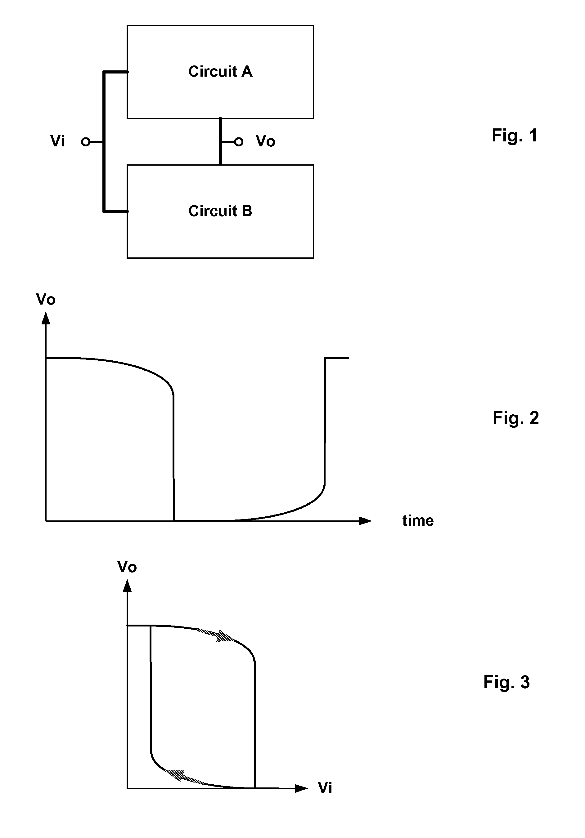
OSCILLATOR WITH FREQUENCY DETERMINED BY RELATIVE MAGNITUDES OF CURRENT SOURCES
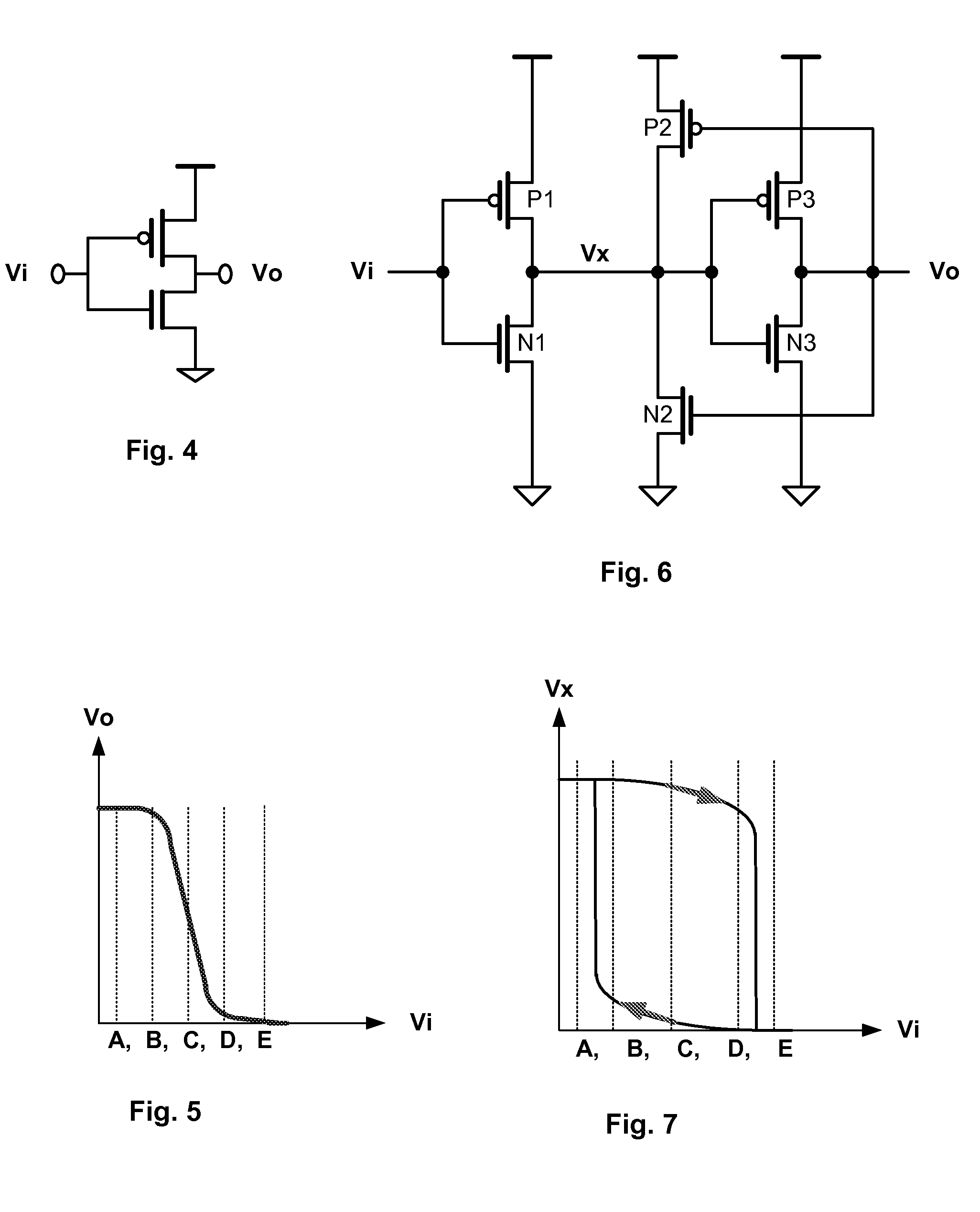
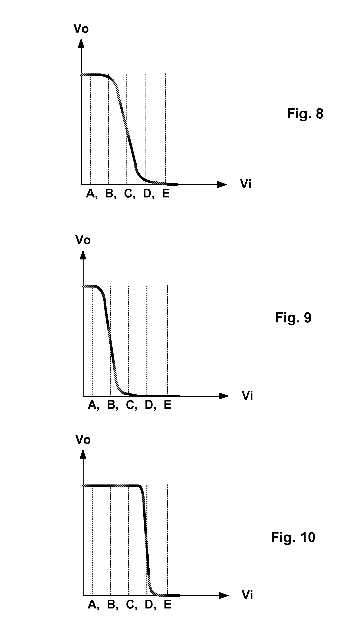
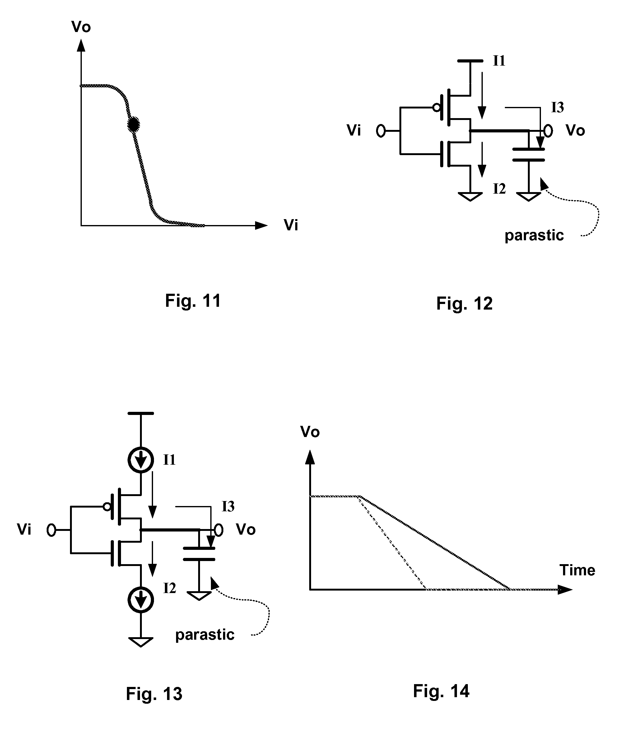
This application is a continuation of U.S. patent application Ser. No. 12/776,198, filed on 7 May 2010 entitled Oscillator With Frequency Determined by Relative Magnitudes of Current Sources. This application is incorporated herein by reference. International Business Machines Corporation, a New York corporation, and Macronix International Corporation, Ltd., a Taiwan corporation are parties to a Joint Research Agreement. BACKGROUND 1. Field of the Invention This technology relates to an oscillator circuit, and in particular an oscillator circuit with a hysteresis circuit, such as a series of cross-coupled inverters, and separately in particular to the inclusion of multiple current sources to simplify the prediction of the oscillator frequency. 2. Description of Related Art Current controlled ring oscillators, with a series of inverters powered by current sources, have a frequency which is difficult to predict, and have a slow transient. The slow transient and the difficulty of predicting the output frequency occur, because despite the inclusion of current sources, the charging and discharging current of an output node in the current controlled oscillator is not determined by a simple relationship to the size of the current sources. Instead, the current controlled ring oscillators has an output frequency which is a complicated and slow function of the sizes of the PMOS and NMOS transistors of the neighboring inverters, mobility, input voltage, etc. One aspect of the technology is an apparatus including an oscillator circuit generating an oscillating signal. The oscillator circuit includes a circuit loop and multiple current sources. The circuit loop includes an output having the oscillating signal. The multiple current sources are turned on independently of a phase of the oscillating signal. The multiple current sources control magnitudes of both charging current and discharging current at nodes of the circuit loop, including the output. Relative magnitudes of different current sources in the multiple current sources determine a frequency of the oscillating signal. In some embodiments, the circuit loop includes multiple series-connected hysteresis circuits. In some embodiment, the nodes connect neighboring hysteresis circuits. In one embodiment, the charging current of the nodes is determined by a current difference between a first current source of a following hysteresis circuit and a second current source of a preceding hysteresis circuit, such that the first current source draws a first current from a high voltage reference and the second current source sinks a second current to a low voltage reference. In another embodiment, the discharging current of the nodes is determined by a current difference between a first current source of a preceding hysteresis circuit and a second current source of a following hysteresis circuit, such that the first current source draws a first current from a high voltage reference and the second current source sinks a second current to a low voltage reference. In some embodiments, the circuit loop includes multiple series-connected cross-coupled inverters. In some embodiments, the nodes connect neighboring cross-coupled inverters of the plurality of series-connected cross-coupled inverters. In one embodiment, the charging current of the nodes is determined by a current difference between a first current source of a following cross-coupled inverter and a second current source of a preceding cross-coupled inverter, such that the first current source draws a first current from a high voltage reference and the second current source sinks a second current to a low voltage reference. In another embodiment, the discharging current of the nodes is determined by a current difference between a first current source of a preceding cross-coupled inverter and a second current source of a following cross-coupled inverter, such that the first current source draws a first current from a high voltage reference and the second current source sinks a second current to a low voltage reference. In some embodiments, the cross-coupled inverters include a first inverter and a second inverter, such that the first inverter has an output connected to an input of the second inverter, the second inverter has an output connected to an input of the first inverter, the input of the first inverter is responsive to a preceding signal from a preceding cross-coupled inverter, and the output of the first inverter sends a following signal to a following cross-coupled inverter. In one embodiment, the relative magnitudes of the different current sources determine the frequency of the oscillating signal, in that the relative magnitudes of the different current sources include a current ratio of a first current source of the first inverter to a second current source of the second inverter, the first current source and the second current source drawing current from a high voltage reference. In another embodiment, the relative magnitudes of the different current sources determine the frequency of the oscillating signal, in that the relative magnitudes of the different current sources include a current ratio of a first current source of the first inverter to a second current source of the second inverter, the first current source and the second current source sinking current to a low voltage reference. In various embodiments, the oscillating signal is a triangle wave. In various embodiments, the oscillating signal is a sinusoidal wave. Another aspect of the technology is a method, comprising the steps: generating an oscillating signal from an output of a circuit loop, the frequency of the oscillating signal determined by relative magnitudes of different current sources in a plurality of current sources, the plurality of current sources turned on independently of a phase of the oscillating signal, the plurality of current sources controlling magnitudes of both charging current and discharging current at nodes of the circuit loop. Circuit A performs the pull up, and Circuit B performs the pull down. An example of Circuit A is a current source that sources current from a high voltage reference, and an example of Circuit B is a current source that sinks current to a low voltage reference The transient is slow at the beginning, and then fast at the end. It appears to be the overlapped version of the rising and falling time domain curves, adjusted as functions of the input voltage. Hysteresis is created by making the signal hard to transition or slower in one direction than the other direction. The transition from point A to point E occurs as follows: At A: Vi=0.1, Vo=1 At B: Vi=0.3, Vo=1 At C: Vi=0.5, Vo=0.5 At D: Vi=0.7, Vo=0 At E: Vi=0.9, Vo=0 The opposite transition from point E to point A is exactly the same as listed above, but in the opposite order. For simplicity, in some embodiments with a series of hysteresis circuits, the hysteresis circuit refers to the cross-coupled inverters, but without the preceding inverter circuit, there is no hysteresis. The transition from point A to point E occurs as follows: At A: Vi=0.1, Vo=1 At B: Vi=0.3, Vo=1 At C: Vi=0.5, Vo=0.9 At D: Vi=0.7, Vo=0.7 At E: Vi=0.9, Vo=0 However, the opposite transition from point E to point A occurs as follows: At E: Vi=0.9, Vo=0 At B: Vi=0.7, Vo=0 At C: Vi=0.5, Vo=0.1 At D: Vi=0.3, Vo=0.3 At E: Vi=0.1, Vo=1 Because the transition between point A and point E depends on the direction, there is hysteresis. The hysteresis curve of At the beginning, say Vi=0, Vx=1, Vo=0 Vi=0.1
Vi=0.3
Vi=0.5
Vi=0.7
Vi=0.9
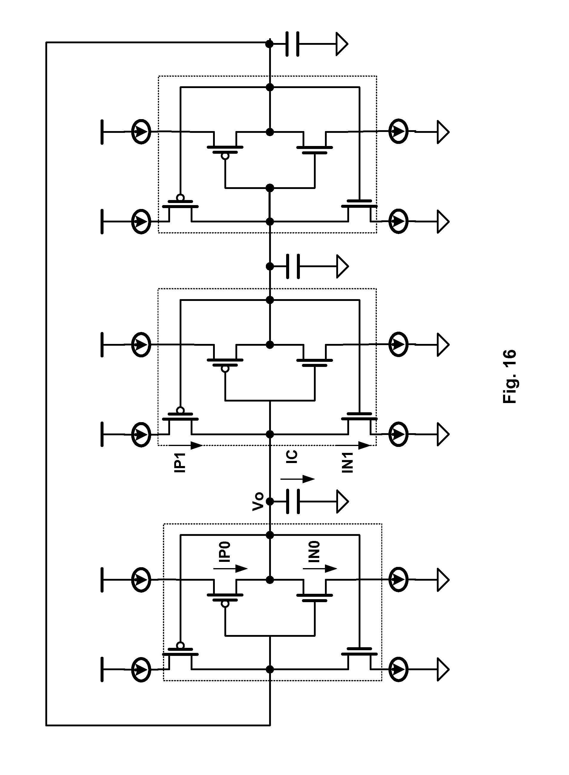
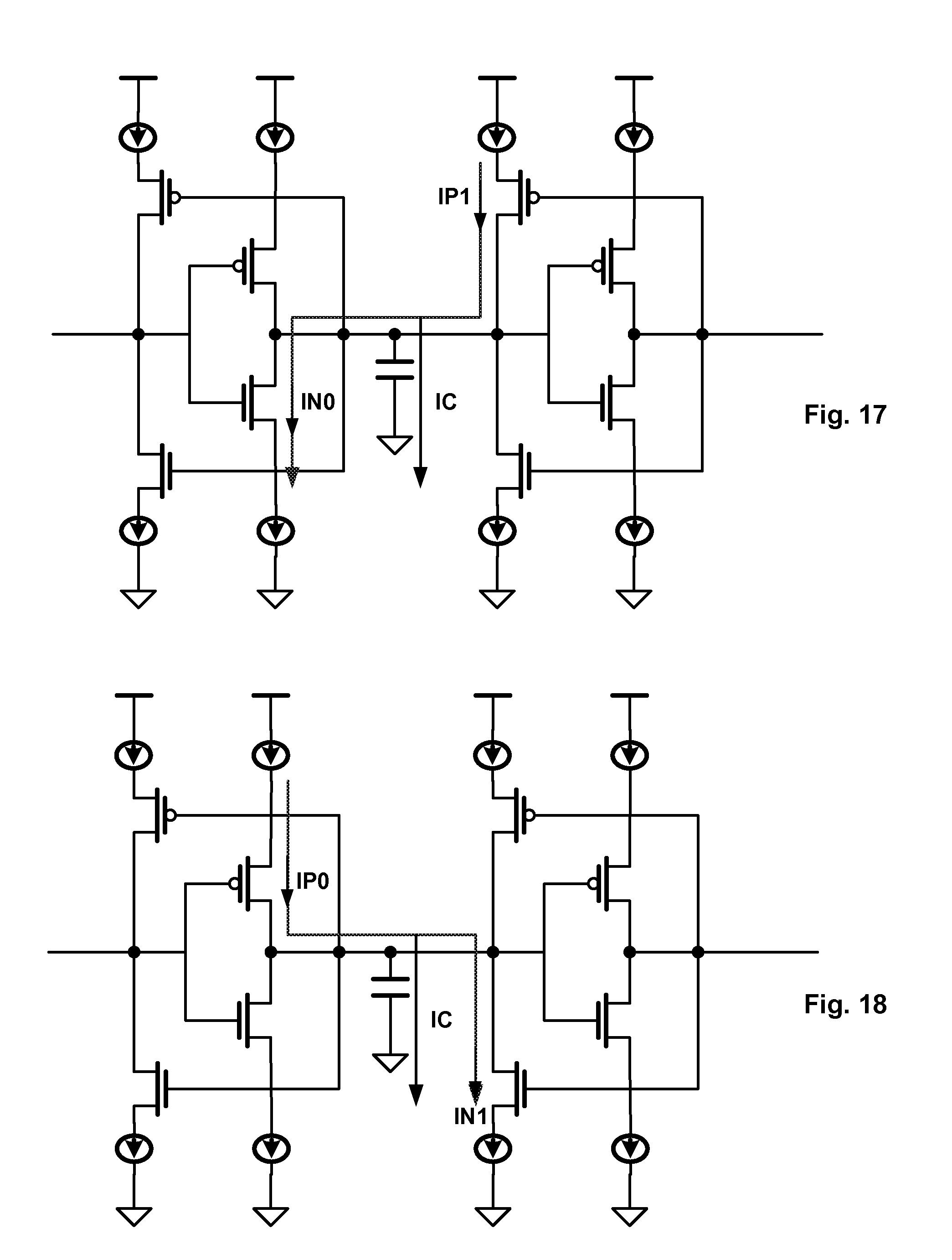
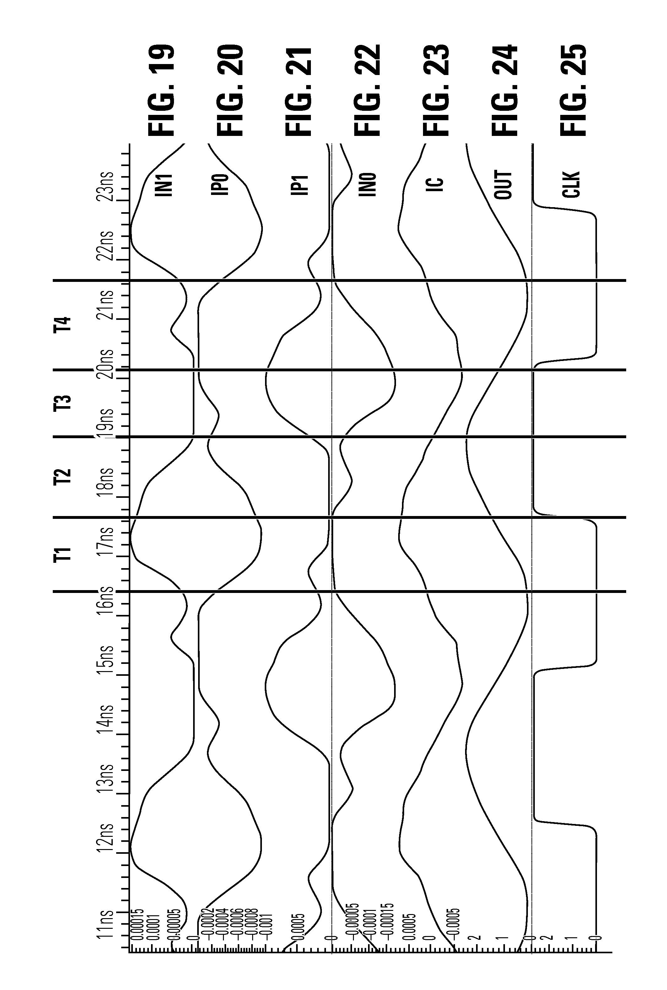
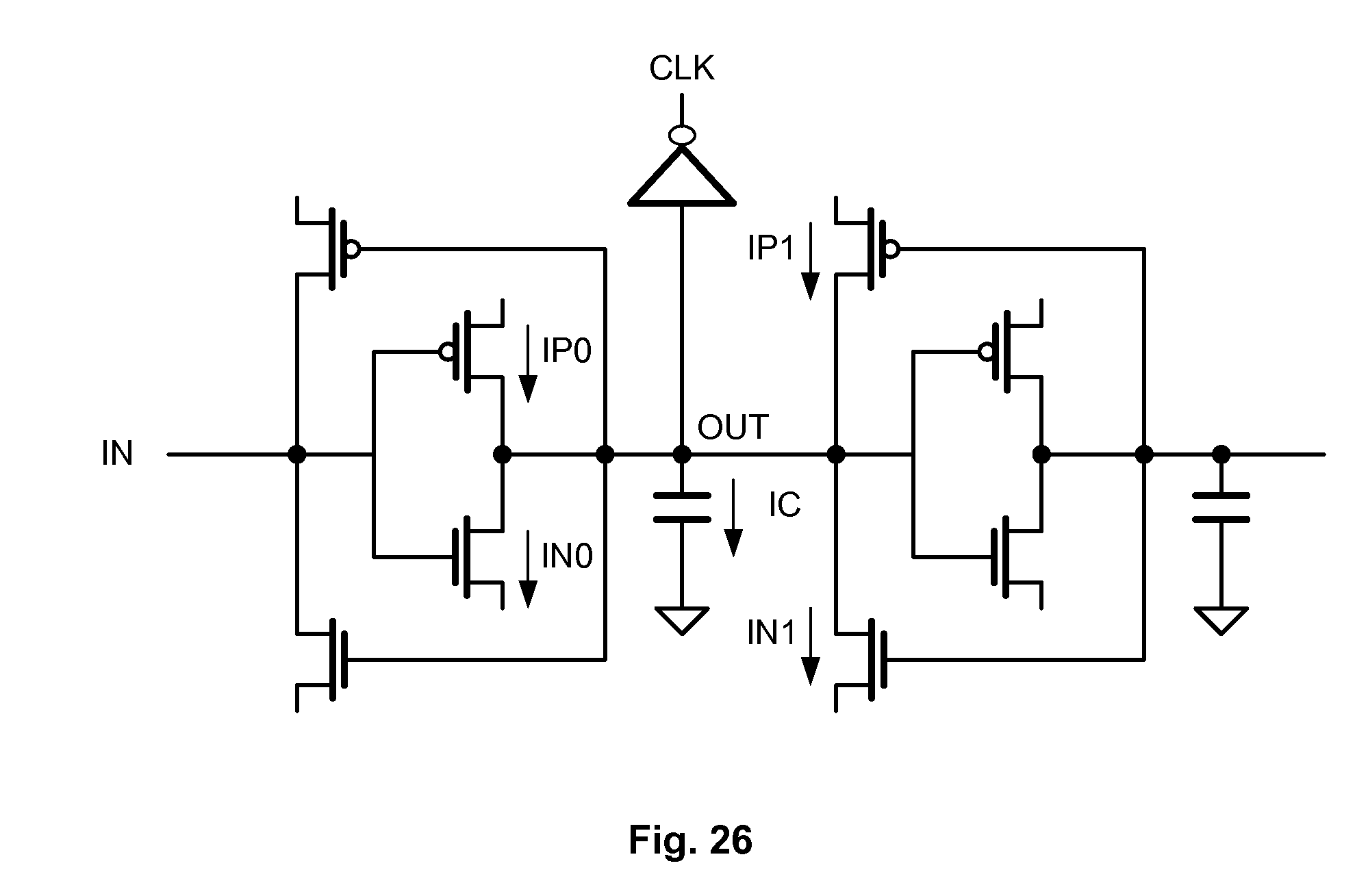
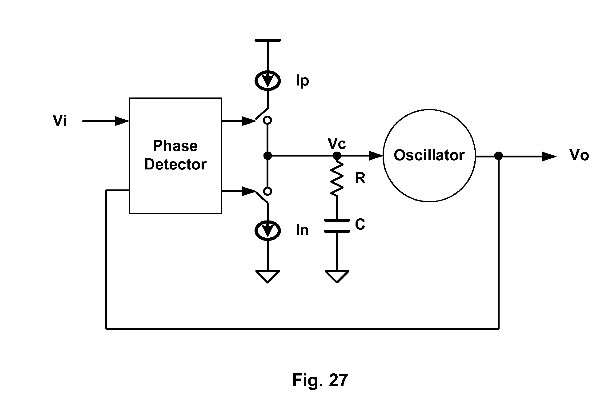
The ratio of the PMOS and NMOS controls the transient point. In In In The transient point is controllable by adjusting the P and N wells. There are three currents I3=I1−I2. The three currents are predictable if they are practically simple to calculate. The added current sources attempt to control the rising and falling time of the inverter by setting the transient current to I1 for charging current and I2 for discharging current. Unfortunately, the transient does not follow the dashed line, as would be the case if the added current sources dominated the transient current. Instead, despite the added current sources, the actual transient follows the slower solid line. The transient is slower than expected. The reason is that although I1 and I2 determine the transient speed on he PMOS and NMOS during charging and discharging Vo, the I3 current through the capacitance is too small. For the purposes of predictability, although the equation is I3=I1−I2, the actual value of I3 is complicated to calculate, because the current I3 is related to size, Vi, mobility, etc. Accordingly, there are two problems: slow transient speed, and lack of predictability. Various embodiments add current sources to address both problems. The circuit demonstrates current flow during the charging and discharging phases. Assume V1=1, Vo=0, V2=1 (V2=1 will make V1 go low like and inverter, and oscillation results.) When Vo is at charging phase, ideally, IC is the charging current IC=IP1−IN0. But this is not the case. When Vo is at discharging phase, ideally, IC is the discharging current=IN1−IP0. But this is not the case. The current sources simplify prediction of the charging current and discharging current according to The technology adds high controllability to the frequency of a ring oscillator without phase detection. A typical application is medium-high frequency (100 MHz˜1 GHz) operation. I*T=C*V, where I is current, T is period, C is capacitance, and V is peak voltage. There are 4 variables. With a regulated V, C significantly larger than parasitic capacitance, then an accurate I determines 3 variables of the 4 variables, thereby making predictable the remaining 4th variable of T (or Frequency). Accordingly, this technology accurately controls the current. Because C and V are also controlled, the current control also controls the frequency. The following is an example of determining the current to achieve a 250 MHz (4 nS) oscillator signal. V=2.5 V and regulated. Other voltages are possible. C=250 fF, significant larger than parasitic capacitance. The goal is T=2 ns, which represents a half cycle, corresponding to either the charging half cycle or the discharging half cycle. According to the equation, the controlled current should be I=312.5 uA or about 300 uA. So peak current of IC should be 600 uA or higher, due to parasitic capacitance. This current comes from current reference system. In the following equations, I1 is for short for IP1 or IN1; I0 is for short for IP0 or IN0. I1=600 uA, I0=0 uA, I1:I0=infinite; means not physical. I1=700 uA, I0=100 uA, I1:I0=7:1; too large a ratio is hard to current match, but saves some power I1=800 uA, I0=200 uA, I1:I0=4:1 I1=1.2 mA, I0=400 uA, I1:I0=3:1; current consumption is getting larger and not so much gain from ratio. In the preceding example calculation, the ratio of the current sources corresponding to IP1 and IN0 is 4:1, and the ratio of the current sources corresponding to IN1 and IP0 is 4:1. Similarly, the difference between the current sources corresponding to IP1 and IN0 is 600 uA, and the difference between the current sources corresponding to IN1 and IP0 is 600 uA. In other embodiments, other current ratios are possible. The values of IP0, IP1, IN0 and IN1 are controllable by a trimmed bias or a phase detector. The ideal load capacitance CL varies with whether a phase detector is used. With a phase detector, load capacitance CL could be zero for saving power, and increase the oscillator frequency into the GHz range. Without a phase detector, load capacitance CL should be as large as possible, to avoid process variation, at the cost of more power consumption. During the charging phase, the average charging current IC=K*(IP1−IN0) K is a constant. K=½ for triangle current waveform. During the discharge phase, the average discharging current IC=K*(IN1−IP0) Again, K is a constant. K=½ for triangle current waveform. At a lower frequency range, where the output waveform is triangular, (x−y) represents a relative magnitude of the current sources, such as (800 uA-200 uA). (Vd−Vs) represents a difference between the high voltage reference and the low voltage reference. The current sources source current from the high voltage reference Vd and sink current to the low voltage reference Vs. Frequency=1/T (units in Hertz) In both T1 and T2, the output node OUT has a discharging current of IN1-IP0, and IP1 and IN0 are almost off. Because IP1 and IN0 are almost off, their contribution can be practically ignored for predicting the oscillator frequency. In both T3 and T4, the output node OUT has a charging current of IP1-IN0, and IP0 and IN1 are almost off. Because IP0 and IN1 are almost off, their contribution can be practically ignored for predicting the oscillator frequency. An improved voltage controllable oscillator includes the improved oscillator technology herein. The voltage controllable oscillator includes a phase detector and a charge pump circuit. The charge pump circuit includes 2 current sources Ip, resistor R, and capacitor C. Other embodiments include CCO (current controllable oscillator) and RCO (resistor controllable oscillator) While the present invention is disclosed by reference to the preferred embodiments and examples detailed above, it is to be understood that these examples are intended in an illustrative rather than in a limiting sense. It is contemplated that modifications and combinations will readily occur to those skilled in the art, which modifications and combinations will be within the spirit of the invention and the scope of the following claims. An oscillator circuit includes a circuit loop and multiple current sources. The circuit loop includes an output having the oscillating signal. The multiple current sources are turned on independently of a phase of the oscillating signal. The current sources control magnitudes of both charging current and discharging current at nodes of the circuit loop, including the output. Relative magnitudes of different current sources determine a frequency of the oscillating signal. 1. An apparatus, comprising:
an oscillator circuit generating an oscillating signal, comprising:
a circuit loop including an output having the oscillating signal; and a plurality of current sources turned on independently of a phase of the oscillating signal, the plurality of current sources controlling magnitudes of both charging current and discharging current at nodes of the circuit loop, the nodes including the output, the plurality of current sources including different current sources, wherein relative magnitudes of the different current sources controlling current flow through different cross-coupled circuits of a plurality of series-connected cross-coupled circuits in the circuit loop determine a frequency of the oscillating signal. 2. The apparatus of 3. The apparatus of 4. The apparatus of 5. The apparatus of 6. The apparatus of the cross-coupled inverters include a first inverter and a second inverter, such that the first inverter has an output connected to an input of the second inverter, the second inverter has an output connected to an input of the first inverter, the input of the first inverter is responsive to a preceding signal from a preceding cross-coupled inverter, and the output of the first inverter sends a following signal to a following cross-coupled inverter, wherein the relative magnitudes of the different current sources in the plurality of current sources determine the frequency of the oscillating signal, in that the relative magnitudes of the different current sources include a current ratio of a first current source of the first inverter to a second current source of the second inverter, the first current source and the second current source drawing current from a high voltage reference. 7. The apparatus of the cross-coupled inverters include a first inverter and a second inverter, such that the first inverter has an output connected to an input of the second inverter, the second inverter has an output connected to an input of the first inverter, the input of the first inverter is responsive to a preceding signal from a preceding cross-coupled inverter, and the output of the first inverter sends a following signal to a following cross-coupled inverter, wherein the relative magnitudes of the different current sources in the plurality of current sources determine the frequency of the oscillating signal, in that the relative magnitudes of the different current sources include a current ratio of a first current source of the first inverter to a second current source of the second inverter, the first current source and the second current source sinking current to a low voltage reference. 8. The apparatus of 9. The apparatus of 10. A method, comprising:
generating an oscillating signal from an output of a circuit loop, the frequency of the oscillating signal determined by relative magnitudes of different current sources controlling current flow through different cross-coupled circuits of a plurality of series-connected cross-coupled circuits in the circuit loop, the different current sources in a plurality of current sources turned on independently of a phase of the oscillating signal, the plurality of current sources controlling magnitudes of both charging current and discharging current at nodes of the circuit loop. 11. The method of 12. The method of 13. The method of 14. The method of 15. The method of the cross-coupled inverters include a first inverter and a second inverter, such that the first inverter has an output connected to an input of the second inverter, the second inverter has an output connected to an input of the first inverter, the input of the first inverter is responsive to a preceding signal from a preceding cross-coupled inverter, and the output of the first inverter sends a following signal to a following cross-coupled inverter, wherein the relative magnitudes of the different current sources in the plurality of current sources determine the frequency of the oscillating signal, in that the relative magnitudes of the different current sources include a current ratio of a first current source of the first inverter to a second current source of the second inverter, the first current source and the second current source drawing current from a high voltage reference. 16. The method of the cross-coupled inverters include a first inverter and a second inverter, such that the first inverter has an output connected to an input of the second inverter, the second inverter has an output connected to an input of the first inverter, the input of the first inverter is responsive to a preceding signal from a preceding cross-coupled inverter, and the output of the first inverter sends a following signal to a following cross-coupled inverter, wherein the relative magnitudes of the different current sources in the plurality of current sources determine the frequency of the oscillating signal, in that the relative magnitudes of the different current sources include a current ratio of a first current source of the first inverter to a second current source of the second inverter, the first current source and the second current source sinking current to a low voltage reference. 17. The method of 18. The method of 19. An apparatus, comprising:
an oscillator circuit generating an oscillating signal, comprising:
a circuit loop including a plurality of series-connected cross-coupled circuits and an output outputting the oscillating signal; and a plurality of current sources, being turned on independently of a phase of the oscillating signal, controlling different current flows through different cross-coupled circuits of the plurality of series-connected cross-coupled circuits. 20. The apparatus of RELATED APPLICATIONS
PARTIES TO A JOINT RESEARCH AGREEMENT
SUMMARY
BRIEF DESCRIPTION OF THE DRAWINGS
DETAILED DESCRIPTION