HIGH SPEED MODULAR JACK HAVING WRAPPING TRANSFORMERS
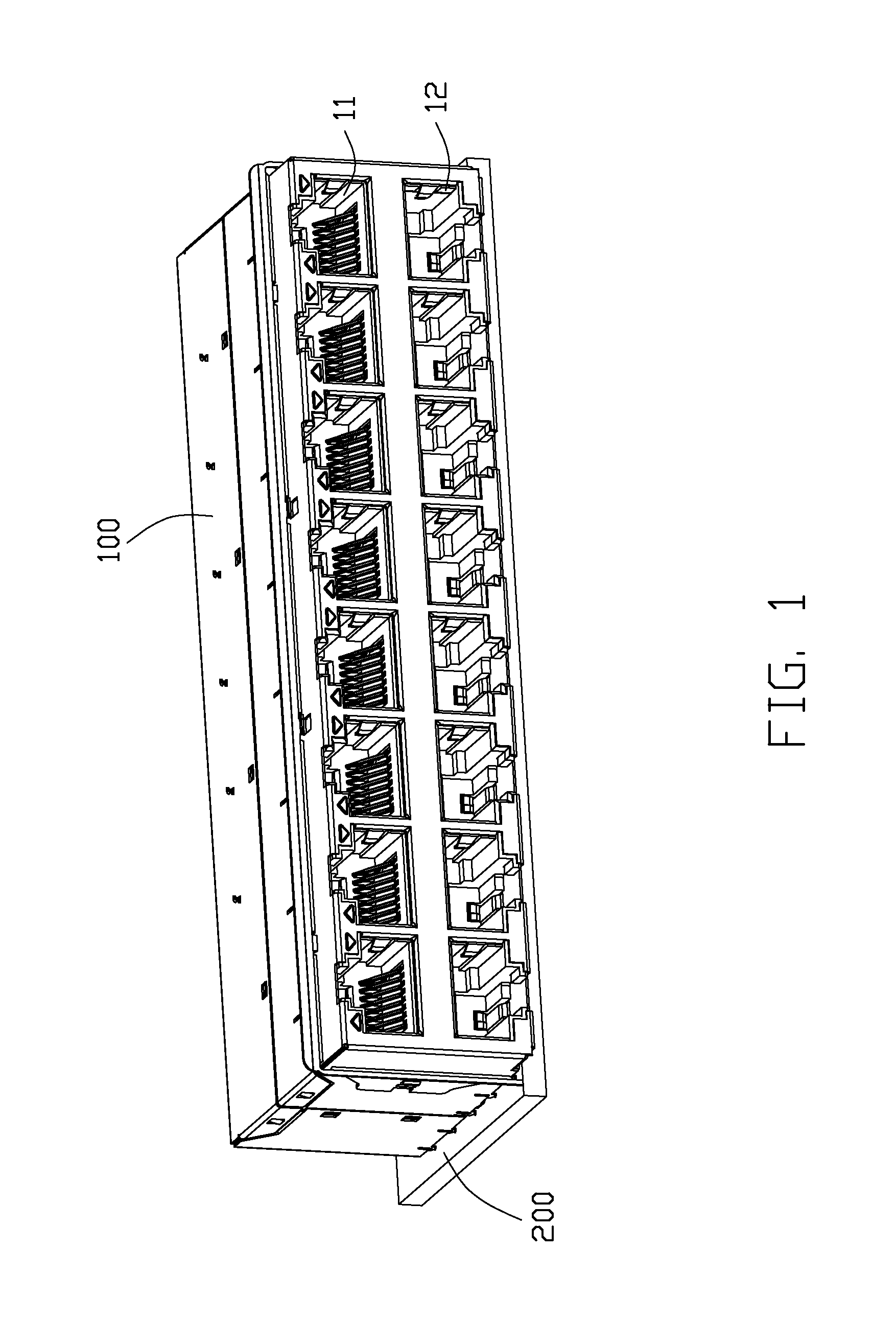
1. Field of the Invention The present invention relates to a modular jack suitable for high-speed communication, and more particularly to a RJ45 receptacle connector having wrapping transformers. 2. Description of Related Art U.S. Patent Application Publication No. 2012/0309233, published on Dec. 6, 2012, discloses a modular jack used for 10 Gbps Ethernet. The modular jack includes an insulative housing with a mounting port and a row of insert modules inserted into the mounting port along a back-to-front direction. Each insert module has a PCBA (printed circuit board assembly) and a terminal module located below the PCBA. The terminal module includes an insulative carrier having a receiving chamber and a plurality of wrapping transformers and chokes in the receiving chamber. Each transformer has a magnetic core and a plurality of coils wound around the magnetic core. Ends of the coils are wrapped to the terminals for further connection. U.S. Patent Application Publication No. 2012/0196479, published on Aug. 2, 2012, discloses a modular jack used for 10 Gbps Ethernet. The modular jack includes an insulative housing with a mounting port and a row of insert modules inserted into the mounting port along a back-to-front direction. Each insert module has two vertical PCBAs, a middle bracket sandwiched between the PCBAs, a mating contact module mounted to the middle bracket along a front-to-back direction, and a bottom terminal module mounted to the middle bracket along a bottom-to-top direction. Each PCBA includes a vertical PCB (printed circuit board) and a plurality of isolation transformers mounted to the vertical PCB. Each transformer includes a magnetic core and a plurality of coils wound around the magnetic core. Ends of the coils are soldered to the vertical PCB through an automatic machine. This modular jack has many components which add costs to manufacturing. Hence, a modular jack having a simple structure is desired. Accordingly, an object of the present invention is to provide a modular jack having a simple structure. In order to achieve the object set forth, the invention provides a modular jack comprising an insulative housing and an insert module. The insulative housing defines a lower port, an upper port stacked on the lower port, and a mounting port located behind the lower and upper ports. The insert module is mounted to the insulative housing from the mounting port to the lower and upper ports along a back-to-front direction. Each of the lower and upper ports is used for mating with a modular plug connector. The insert module comprises a printed circuit broad assembly (PCBA) disposed horizontally in the mounting port and a terminal module located below the PCBA. The PCBA includes a top face, a bottom face, a set of upper contacts each having an upper contacting portion extending backwardly and upwardly in the upper port and an upper connecting portion mounted on the top face, a set of lower contacts each having a lower contacting portion extending backwardly and downwardly in the lower port and a connecting portion mounted on the bottom face, and a plurality of isolation transformers mounted on the top and bottom faces. The terminal module has a set of first terminals electrically connected to the upper contacts through the PCBA and a set of second terminals electrically connected to the lower contacts through the PCBA. The first and second terminals are used to mount to an exterior substrate. The isolation transformers are disposed on the horizontal PCBA for automatically soldering and saving room. This modular jack has few parts that the structure of this modular jack is simple. The cost of manufacturing the modular jack is decreased comprising to above references. Other objects, advantages and novel features of the invention will become more apparent from the following detailed description when taken in conjunction with the accompanying drawings. Reference will now be made in detail to the preferred embodiment of the present invention. Referring to Referring to Referring to Referring to The PCBA 20 includes an upper plastic body 207, a set of upper contacts 205 insert molded with the upper plastic body 207, a lower plastic body 208, and a set of lower contacts 206 insert molded with the lower plastic body 208. The upper plastic body 207 is mounted on the top face 2011 and each upper contact 205 is soldered on the top face 2011. The lower plastic body 208 is mounted on the bottom face 2021 and each lower contact 206 is soldered on the bottom face 2021. Each upper contact 205 has an upper contacting portion 2052 extending backwardly and upwardly in the upper port 11 and a connecting portion 2051 surface mounted on a front portion of the top face 2011. Each lower contact 206 has a lower contacting portion 2062 extending backwardly and downwardly in the lower port 12 and a connecting portion (not labeled) surface mounted on a front portion of the bottom face 2021. Referring to The terminal module 21 includes a set of first terminals 211 connected with the upper PCB 201, a set of second terminals 212 connected with the lower PCB 202, and a metal shielding plate 213 disposed between the first and second terminals 211, 212. The upper contacts 205 electrically connect with corresponding first terminals 211 through the upper PCB 201 and the upper transformers 203. The lower contacts 206 electrically connect with corresponding second terminals 212 through the lower PCB 202 and the lower transformers 204. The metal shielding plate 213 is used for shielding electromagnetic interference (EMI) between the first and second terminals when they transmitting signals. The terminal module 21 has a first insulative carrier 214 for retention of the first terminals 211 and a second insulative carrier 215 for retention of the second terminals 212. The metal shielding plate 213 is sandwiched between the first and second insulative carriers 214, 215. There is a receiving chamber 216 defined by the first insulative carrier 214 and the second insulative carrier 215. The lower transformers 204 mounted on the lower PCB 202 are received in the receiving chamber 216. The first insulative carrier 214 has a first receiving chamber 2141 and the second insulative carrier 215 has a second receiving chamber 2151. The first receiving chamber 2141 and the second receiving chamber 2151 assembled to form the receiving chamber 216. The first insulative carrier 214 has a first post 2142 mounting into a through hole 209 of the upper PCB 201. The second insulative carrier 215 has a second post 2152 mounting a through hole (not labeled) of the lower PCB 202. The first insulative carrier 214 has a positioning post 2143 and the second insulative carrier 215 has a positioning hole 2153 for the positioning post 2143 inserting therein. Each first terminal 211 includes a first connecting portion 2111 connecting with the upper PCB 201, a first holding portion 2112 held by the first insulative carrier 214, and a first mounting portion 2113 located below the bottom PCB 4. The second terminal 212 includes a second connecting portion 2121 connecting with the lower PCB 201, a second holding portion 2122 held by the second insulative carrier 215, and a second mounting portion 2123 located below the bottom PCB 4. The first mounting portion 2113 and the second mounting portion 2123 are used for electrically and mechanically engagement with the horizontal mother PCB 200. The first insulative carrier 214 has a first supporting face 2146 and a second supporting face 2147 located below the first supporting face 2146. The second carrier 215 having a third supporting face 2157 disposed at a same level with the second supporting face 2147. The upper PCB 201 is supported by the first supporting face 2146 and the lower PCB 202. The lower PCB 202 is supported by the second face 2147 and the third supporting face 2157. The metal shielding plate 213 has a main body portion 2130, a top inserting section 2131 extending upwardly from the main body portion 2130, and a mounting portion 2134 extending downwardly from the main body portion 2130. The main body portion 2130 defines two holes 20133 for the positioning post 2143 passing over. The mounting portions 2134 are used for electrically and mechanically engagement with the horizontal mother board 200. The top inserting section 2131 is inserted into the first cutout 2013 and the second cutout 2023. The top inserting section 2131 is soldered to the upper PCB 201 and the lower PCB 202 by only one process. Referring to Referring to It is to be understood, however, that even though numerous characteristics and advantages of the present invention have been set forth in the foregoing description, together with details of the structure and function of the invention, the disclosure is illustrative only, and changes may be made in detail, especially in matters of shape, size, and arrangement of parts within the principles of the invention to the full extent indicated by the broad general meaning of the members in which the appended claims are expressed. A modular jack includes an insulative housing and an insert module mounted from the mounting port to the insulative housing along a back-to-front direction. The insulative housing defines a lower port, an upper port stacked on the lower port, and a mounting port located behind the lower and upper ports. Each of the lower and upper ports is used for mating with a modular plug connector. The insert module comprises a printed circuit broad assembly (PCBA) disposed horizontally in the mounting port and a terminal module located below the PCBA. The PCBA includes a top face, a bottom face, a set of upper contacts each having an upper contacting portion extending in the upper port, a set of lower contacts each having a lower contacting portion extending in the lower port, and a plurality of isolation transformers mounted on the top and bottom faces. 1. A modular jack comprising:
an insulative housing defining a lower port, an upper port stacked on the lower port, and a mounting port located behind the lower and upper ports; and an insert module mounted from the mounting port to the lower and upper ports along a back-to-front direction, the insert module comprising:
a printed circuit broad assembly (PCBA) disposed horizontally in the mounting port, the PCBA includes a top face, a bottom face, a set of upper contacts each having an upper contacting portion extending backwardly and upwardly in the upper port and an upper connecting portion mounted on the top face, a set of lower contacts each having a lower contacting portion extending backwardly and downwardly in the lower port and a connecting portion mounted on the bottom face, and a plurality of isolation transformers mounted on the top and bottom faces; and a terminal module located below the PCBA, the terminal module having a set of first terminals electrically connected to the upper contacts through the PCBA and a set of second terminals electrically connected to the lower contacts through the PCBA, the first and second terminals adapted for mounting to an exterior substrate. 2. The modular jack as claimed in 3. The modular jack as claimed in 4. The modular jack as claimed in 5. The modular jack as claimed in 6. The modular jack as claimed in 7. The modular jack as claimed in 8. The modular jack as claimed in 9. The modular jack as claimed in 10. The modular jack as claimed in 11. An electrical connector comprising:
an insulative housing defining, along a front-to-back direction, a front mating port with a configuration of RJ 45, and a rear connecting port; an insert module forwardly assembled into the housing along said front-to-back direction and including: a printed circuit board assembly (PCBA) including:
at least one printed circuit board extending in a horizontal plane defined by said front-to-back direction and a transverse direction perpendicular to said front-to-back direction; a plurality of mating contacts mounted upon a front region of the printed circuit board and extending into the front mating port; and a plurality of transformers mounted upon the printed circuit board; wherein each of said transformers includes magnetic core with coils wound thereon. 12. The electrical connector as claimed in 13. The electrical connector as claimed in 14. The electrical connector as claimed in 15. The electrical connector as claimed in 16. The electrical connector as claimed in 17. An electrical connector comprising:
an insulative housing defining, along a front-to-back direction, a front mating port with a configuration of RJ 45, and a rear connecting port, said front mating port further divided into an upper mating port and a lower mating port in a vertical direction perpendicular to said front-to-back direction; an insert module forwardly assembled into the housing along said front-to-back direction and including: a printed circuit board assembly (PCBA) including:
oppositely stacked upper and lower printed circuit boards each extending in a horizontal plane defined by said front-to-back direction and a transverse direction perpendicular to both said front-to-back direction and said vertical direction; a plurality of upper mating contacts mounted upon a front region of the upper printed circuit board and extending into the upper mating port; a plurality of lower mating contacts mounted upon a front region of the lower printed circuit board and extending into the lower mating port; and a plurality of upper transformers mounted upon the upper printed circuit board; a plurality of lower transformers mounted upon the lower printed circuit board; wherein each of said upper and lower transformers includes magnetic core with coils wound thereon. 18. The electrical connector as claimed in 19. The electrical connector as claimed in 20. The electrical connector as claimed in BACKGROUND OF THE INVENTION
SUMMARY OF THE INVENTION
BRIEF DESCRIPTION OF THE DRAWINGS
DETAILED DESCRIPTION OF THE PREFERRED EMBODIMENT