HIGH SPEED MODULAR JACK HAVING CENTRAL SHIELD
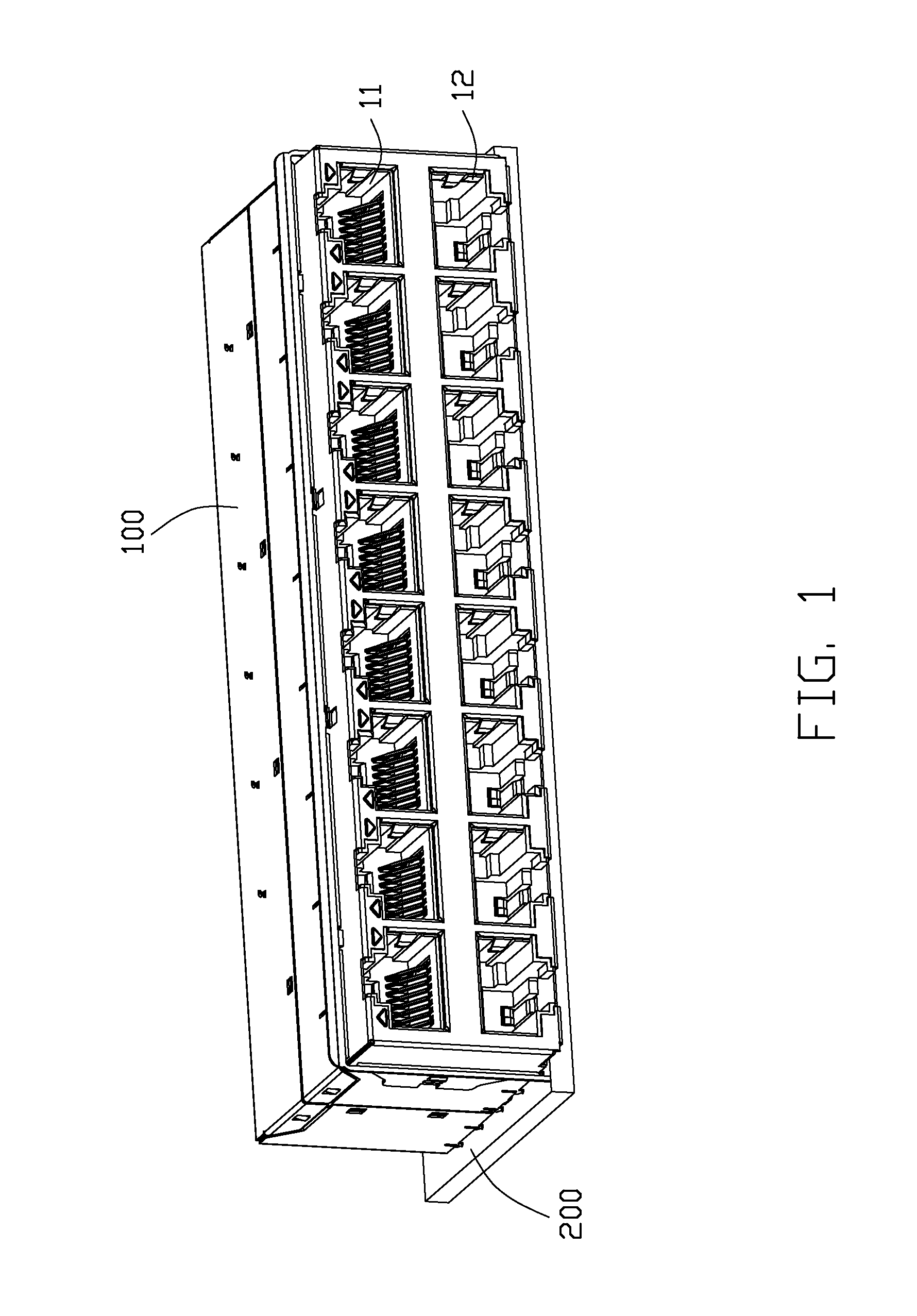
1. Field of the Invention The present invention relates to a modular jack suitable for high-speed communication, and more particularly to a RJ45 receptacle connector having central shields. 2. Description of Related Art U.S. Patent Application Publication No. 2012/0196479, published on Aug. 2, 2012 discloses a modular jack used for 10 Gbps Ethernet. The modular jack includes an insulative housing with a mounting port, a row of insert modules inserted into the mounting port along a back-to-front direction, and a set of central shields each disposed between two adjacent insert modules. The insert module includes two vertical PCBs (printed circuit boards) and a plurality of terminals mounted to bottom portions of the vertical PCBs. Each terminal has a mounting portion for electrically and mechanically engaged with an exterior PCB. The central shield does not engage with the insert modules. When pressing the modular jack to the exterior PCB, force applied to the terminals may not be uniform. U.S. Patent Application Publication No. 2012/0309233, published on Dec. 6, 2012, discloses a modular jack used for 10 Gbps Ethernet. The modular jack includes an insulative housing with a mounting port, a row of insert modules inserted into the mounting port along a back-to-front direction, and a set of central shields each disposed between two adjacent insert modules. Each central shield is made of metal plate with a thin thickness that could not afford a big pressing force. Hence, a modular jack having an improved structure for mounting press-fit terminals is desired. Accordingly, an object of the present invention is to provide a modular jack having a proper structure for mounting press-fit terminals. In order to achieve the object set forth, the invention provides a modular jack including an insulative housing, a set of central shields, and a set of insert modules. The modular jack defines a row of lower ports, a row of upper ports, and a mounting port located behind the lower and upper ports. Each insert module is inserted from the mounting port to corresponding one lower port and one upper port. Each insert module includes a printed circuit broad assembly (PCBA) disposed horizontally in the mounting port and a terminal module located below the PCBA. The PCBA includes a top face, a bottom face, a set of upper contacts each having an upper contacting portion extending backwardly and upwardly in the upper port and an upper connecting portion mounted on the top face, a set of lower contacts each having a lower contacting portion extending backwardly and downwardly in the lower port and a connecting portion mounted on the bottom face. The terminal module has a set of first terminals electrically connected to the upper contacts through the PCBA, a set of second terminals electrically connected to the lower contacts through the PCBA, and an insulative carrier for holding the first and second terminals. Each central shield is disposed between two adjacent insert modules and mounted to the insulative housing. The central shield has a metal wafer and an insulative body holding the metal wafer. The insulative body includes a pressing face extending along a front-to-back direction and the insulative carrier has a receiving pressure face extending along the front-to-back direction. Each terminal has a mounting portion for electrically and mechanically engaged with an exterior PCB. The pressing face transmits a pressure to the receiving pressure face, when pressing the modular jack to the exterior PCB along a top-to-bottom direction. Other objects, advantages and novel features of the invention will become more apparent from the following detailed description when taken in conjunction with the accompanying drawings. Reference will now be made in detail to the preferred embodiment of the present invention. Referring to Referring to Referring to Referring to The PCBA 20 includes an upper plastic body 207, a set of upper contacts 205 insert molded with the upper plastic body 207, a lower plastic body 208, and a set of lower contacts 206 insert molded with the lower plastic body 208. The upper plastic body 207 is mounted on the top face 2011 and each upper contact 205 is soldered on the top face 2011. The lower plastic body 208 is mounted on the bottom face 2021 and each lower contact 206 is soldered on the bottom face 2021. Each upper contact 205 has an upper contacting portion 2052 extending backwardly and upwardly in the upper port 11 and a connecting portion 2051 surface mounted on a front portion of the top face 2011. Each lower contact 206 has a lower contacting portion 2062 extending backwardly and downwardly in the lower port 12 and a connecting portion (not labeled) surface mounted on a front portion of the bottom face 2021. Referring to The terminal module 21 includes a set of first terminals 211 connected with the upper PCB 201, a set of second terminals 212 connected with the lower PCB 202, and a metal shielding plate 213 disposed between the first and second terminals 211, 212. The upper contacts 205 electrically connect with corresponding first terminals 211 through the upper PCB 201 and the upper transformers 203. The lower contacts 206 electrically connect with corresponding second terminals 212 through the lower PCB 202 and the lower transformers 204. The metal shielding plate 213 is used for shielding electromagnetic interference (EMI) between the first and second terminals when they transmitting signals. The terminal module 21 has a first insulative carrier 214 for retention of the first terminals 211 and a second insulative carrier 215 for retention of the second terminals 212. The metal shielding plate 213 is sandwiched between the first and second insulative carriers 214, 215. There is a receiving chamber 216 defined by the first insulative carrier 214 and the second insulative carrier 215. The lower transformers 204 mounted on the lower PCB 202 are received in the receiving chamber 216. The first insulative carrier 214 has a first receiving chamber 2141 and the second insulative carrier 215 has a second receiving chamber 2151. The first receiving chamber 2141 and the second receiving chamber 2151 assembled to form the receiving chamber 216. The first insulative carrier 214 has a first post 2142 mounting into a through hole 209 of the upper PCB 201. The second insulative carrier 215 has a second post 2152 mounting a through hole (not labeled) of the lower PCB 202. The first insulative carrier 214 has a positioning post 2143 and the second insulative carrier 215 has a positioning hole 2153 for the positioning post 2143 inserting therein. Each first terminal 211 includes a first connecting portion 2111 connecting with the upper PCB 201, a first holding portion 2112 held by the first insulative carrier 214, and a first mounting portion 2113 located below the bottom PCB 4. The second terminal 212 includes a second connecting portion 2121 connecting with the lower PCB 201, a second holding portion 2122 held by the second insulative carrier 215, and a second mounting portion 2123 located below the bottom PCB 4. The first mounting portion 2113 and the second mounting portion 2123 are used for electrically and mechanically engagement with the horizontal mother PCB 200. The first insulative carrier 214 has a first supporting face 2146 and a second supporting face 2147 located below the first supporting face 2146. The second carrier 215 having a third supporting face 2157 disposed at a same level with the second supporting face 2147. The upper PCB 201 is supported by the first supporting face 2146 and the lower PCB 202. The lower PCB 202 is supported by the second face 2147 and the third supporting face 2157. The metal shielding plate 213 has a main body portion 2130, a top inserting section 2131 extending upwardly from the main body portion 2130, and a mounting portion 2134 extending downwardly from the main body portion 2130. The main body portion 2130 defines two holes 20133 for the positioning post 2143 passing over. The mounting portions 2134 are used for electrically and mechanically engagement with the horizontal mother board 200. The top inserting section 2131 is inserted into the first cutout 2013 and the second cutout 2023. The top inserting section 2131 is soldered to the upper PCB 201 and the lower PCB 202 by only one process. Referring to Referring to It is to be understood, however, that even though numerous characteristics and advantages of the present invention have been set forth in the foregoing description, together with details of the structure and function of the invention, the disclosure is illustrative only, and changes may be made in detail, especially in matters of shape, size, and arrangement of parts within the principles of the invention to the full extent indicated by the broad general meaning of the members in which the appended claims are expressed. A modular jack includes an insulative housing, a set of central shields, and a set of insert modules. The modular jack defines a mounting port. Each insert module includes a printed circuit broad assembly (PCBA) disposed horizontally in the mounting port and a terminal module located below the PCBA. The terminal module has a set of first terminals, a set of second terminals, and an insulative carrier holding the first and second terminals. Each central shield is disposed between two adjacent insert modules and mounted to the insulative housing. The central shield has a metal wafer and an insulative body for holding the metal wafer. The insulative body includes a pressing face extending along a front-to-back direction and the insulative carrier has a receiving pressure face extending along the front-to-back direction. Each terminal has a mounting portion for electrically and mechanically engaged with an exterior PCB. 1. A modular jack comprising:
an insulative housing defining a row of lower ports, a row of upper ports, and a mounting port located behind the lower and upper ports; a set of insert modules each inserted from the mounting port to corresponding one lower port and one upper port, each insert module including a printed circuit broad assembly (PCBA) disposed horizontally in the mounting port and a terminal module located below the PCBA; the PCBA including a top face, a bottom face, a set of upper contacts each having an upper contacting portion extending backwardly and upwardly in the upper port and an upper connecting portion mounted on the top face, a set of lower contacts each having a lower contacting portion extending backwardly and downwardly in the lower port and a connecting portion mounted on the bottom face; the terminal module having a set of first terminals electrically connected to the upper contacts through the PCBA, a set of second terminals electrically connected to the lower contacts through the PCBA, and an insulative carrier for holding the first and second terminals; and a set of central shields each disposed between two adjacent insert modules and mounted to the insulative housing, the central shield having a metal wafer and an insulative body holding the metal wafer; wherein the insulative body includes a pressing face extending along a front-to-back direction and the insulative carrier has a receiving pressure face extending along the front-to-back direction, each terminal having a mounting portion for electrically and mechanically engaged with an exterior PCB, when pressing the modular jack to the exterior PCB along a top-to-bottom direction, the pressing face transmitting a pressure to the receiving pressure face. 2. The modular jack as claimed in 3. The modular jack as claimed in 4. The modular jack as claimed in 5. The modular jack as claimed in 6. The modular jack as claimed in 7. The modular jack as claimed in 8. The modular jack as claimed in 9. The modular jack as claimed in 10. The modular jack as claimed in 11. A n electrical connector comprising:
an insulative housing defining a front mating portion of an RJ45 configuration, and a rear connecting port along a front-to-back direction; a printed circuit board assembly (PCBA) forwardly assembled into the housing along said front-to-back direction, and including: at least one printed circuit board extending in a horizontal plane defined by the front-to-back direction and a transverse direction perpendicular to said front-to-back direction; a plurality of mating contacts connected to a front region of the printed circuit board and extending into the front mating port; a plurality of electronic components mounted to the printed circuit board; a terminal module mounted to a rear region of and located under the printed circuit board, said terminal module including a plurality of mounting terminals having upper sections upwardly connected to the printed circuit board and lower sections for downwardly connecting to an external printed circuit board on which the housing is seated; wherein the housing and the terminal module are engaged with each other so as to transfer a force imposed upon the housing to the terminal module for efficiently mounting the mounting terminals upon the external printed circuit board. 12. The electrical connector as claimed in 13. The electrical connector as claimed in 14. The electrical connector as claimed in 15. An electrical connector comprising:
an insulative housing defining a front mating port and a rear connecting port along a front-to-back direction, said front mating port further divided into an upper mating port and a lower mating port each being of an RJ 45 configuration; a printed circuit board assembly (PCBA) forwardly assembled into the housing along said front-to-back direction, and including: two stacked printed circuit boards each extending in a horizontal plane defined by the front-to-back direction and a transverse direction perpendicular to said front-to-back direction; a plurality of upper mating contacts connected to a front region of an upper surface of the upper printed circuit board and extending into the upper mating port; a plurality of lower mating contacts connected to a front region of an undersurface of the lower printed circuit board; a plurality of electronic components mounted upon at lest one of the upper printed circuit board and the lower printed circuit board; first and second terminal modules mounted to a rear region of and located under the lower printed circuit board, the first terminal module including a plurality of first mounting terminals having first upper sections upwardly connected to the upper printed circuit board and first lower sections for downwardly connecting to an external printed circuit board on which the housing is seated, the second terminal module including a plurality of second mounting terminals having second upper sections upwardly connected to the lower printed circuit board and second lower sections for downwardly connecting to the external printed circuit board; wherein the housing and each of the terminal module are engaged with each other so as to transfer a force imposed upon the housing to the terminal module for efficiently mounting the mounting terminals upon the external printed circuit board. 16. The electrical connector as claimed in 17. The electrical connector as claimed in 18. The electrical connector as claimed in BACKGROUND OF THE INVENTION
SUMMARY OF THE INVENTION
BRIEF DESCRIPTION OF THE DRAWINGS
DETAILED DESCRIPTION OF THE PREFERRED EMBODIMENT