RADIO FREQUENCY SWITCHING CIRCUITRY WITH REDUCED SWITCHING TIME
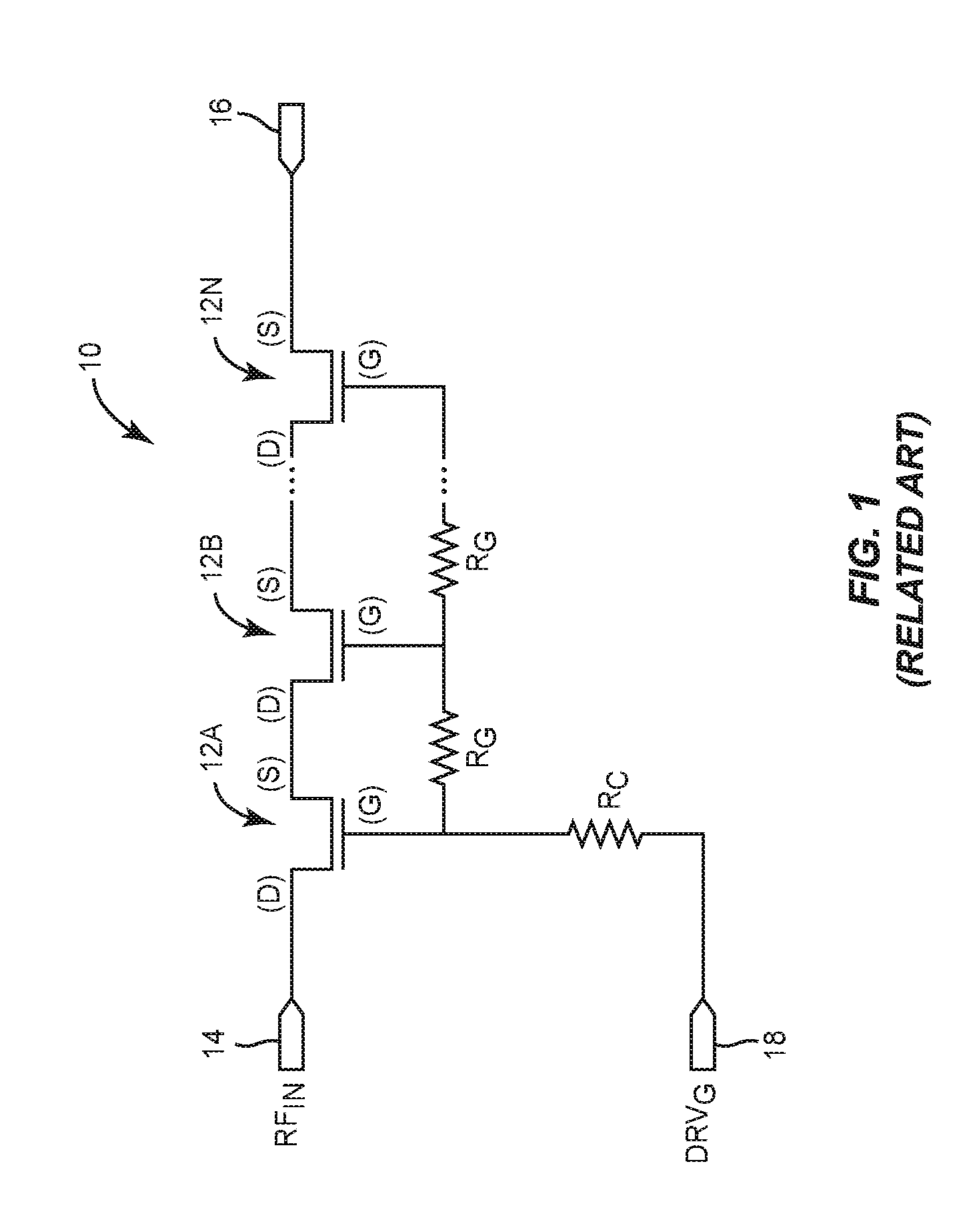
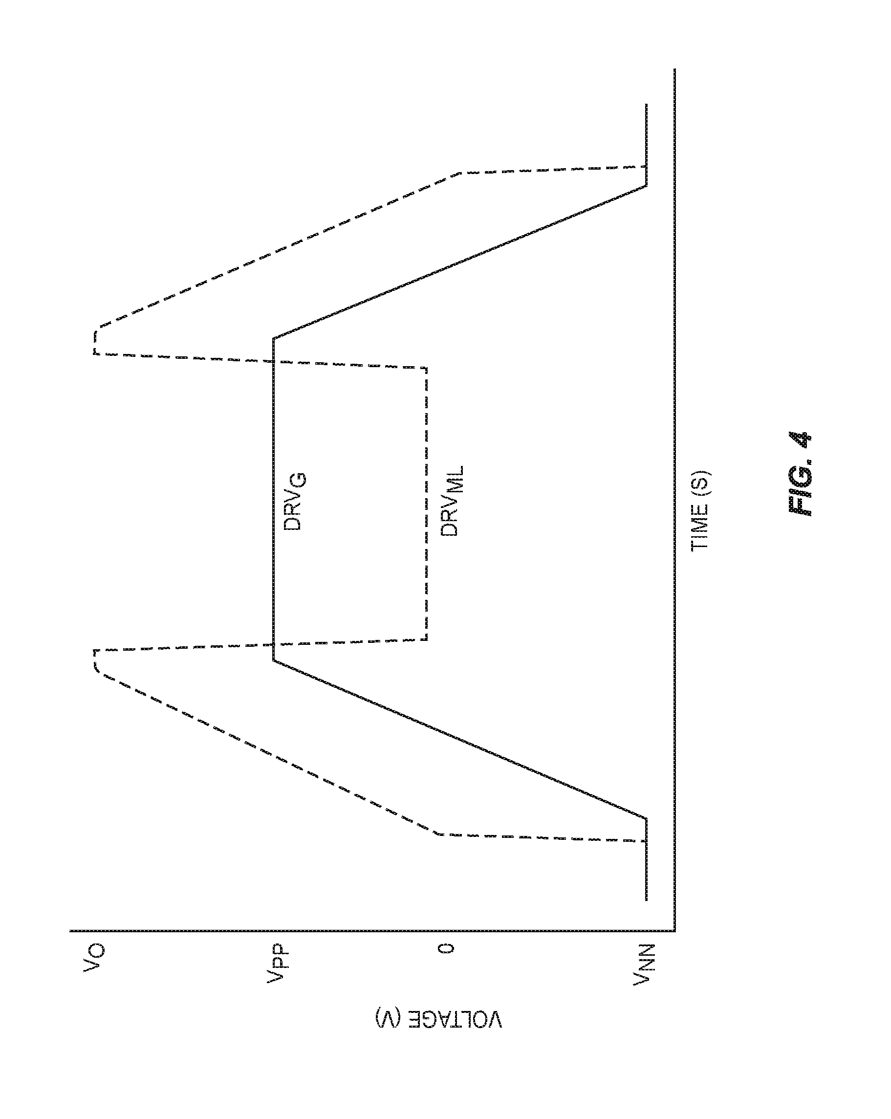
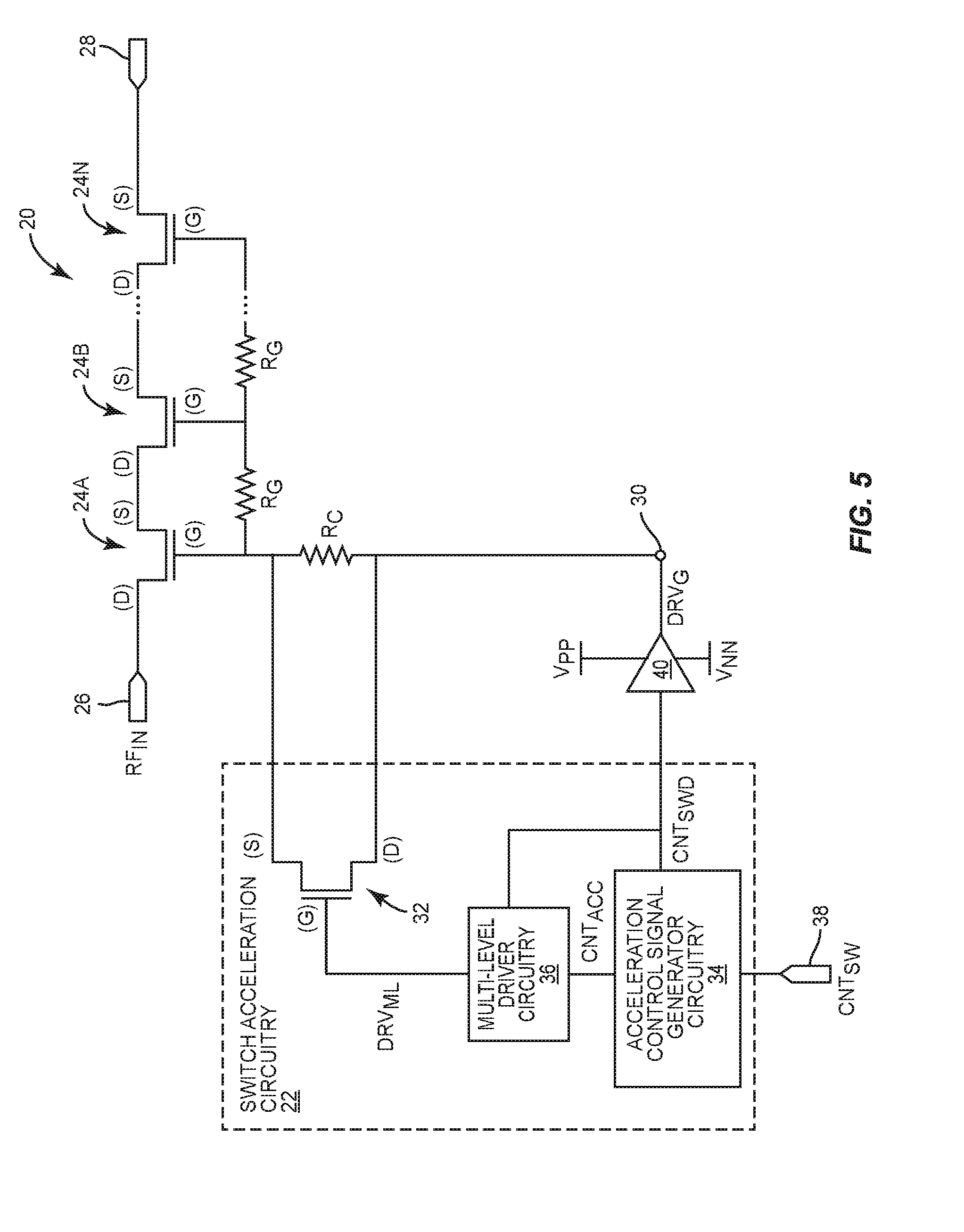
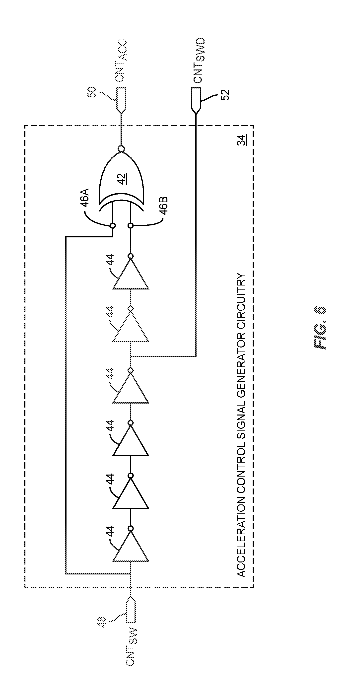
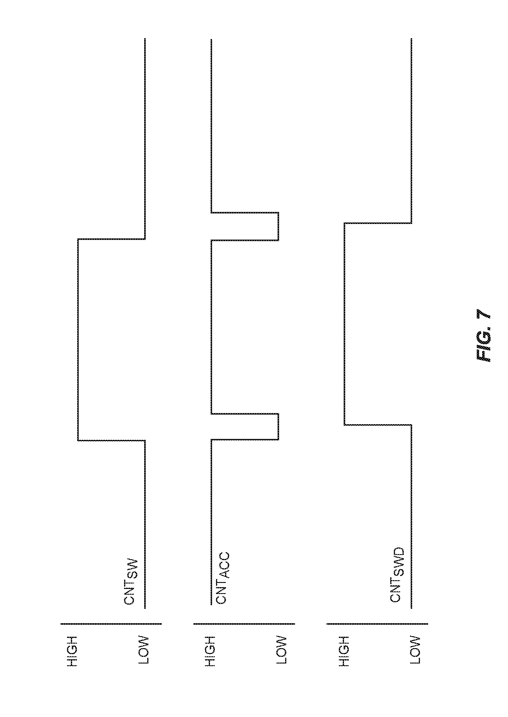
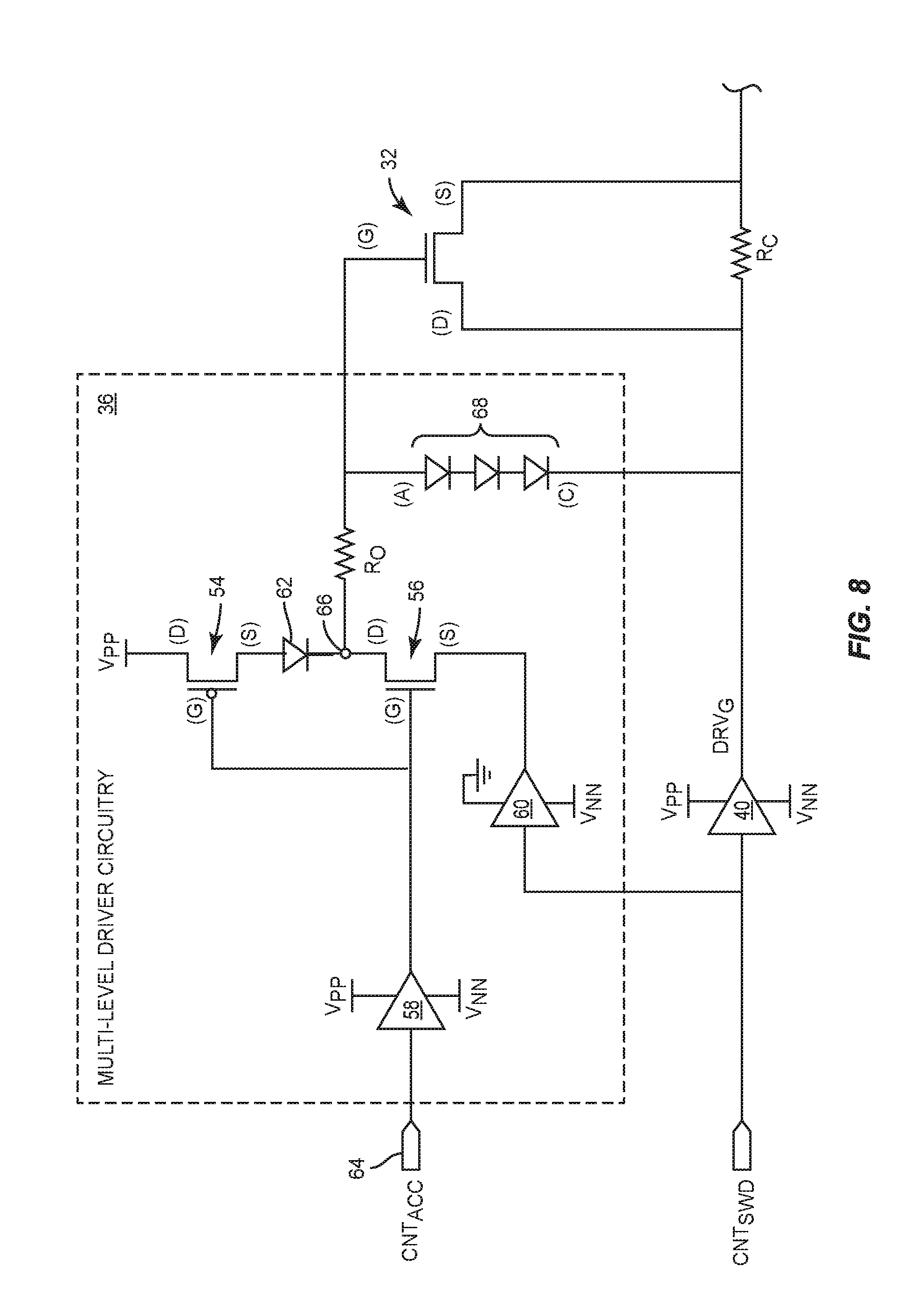
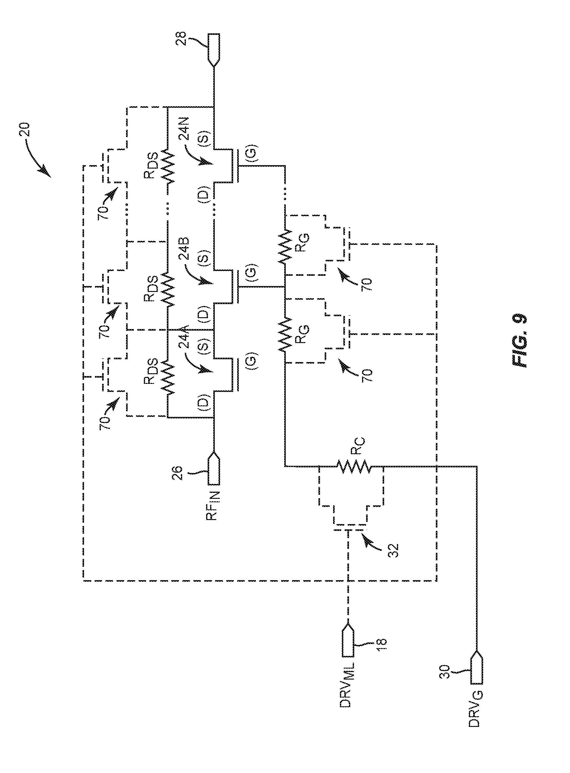
The present disclosure relates to driver circuitry for radio frequency (RF) switching circuitry, and in particular to RF switching circuitry with faster switching times. Radio frequency (RF) switching circuitry is an essential part of any wireless communication device. RF switching circuitry may be used to route RF signals between various nodes (e.g., a power amplifier and an antenna, an antenna and a low noise amplifier (LNA), and the like), to change the impedance of one or more nodes, or any number of other functions. Exemplary RF switching circuitry 10 is shown in A gate drive signal DRVGprovided at the gate drive node 18 places the FETs 12 in one of an on state or an off state. In the on state of the FETs 12, a low impedance path is provided between the input node 14 and the output node 16, thereby allowing an RF input signal RFINat the input node 14 to pass to the output node 16. In the off state of the FETs 12, a high impedance path is provided between the input node 14 and the output node 16, thereby preventing the RF input signal RFINat the input node 14 from reaching the output node 16. The RF switching circuitry 10 may be provided in a series configuration or a shunt configuration. In the series configuration, the input node 14 and the output node 16 are RF signal nodes. In the shunt configuration, the input node 14 is an RF signal node and the output node 16 is a ground node or coupled to a fixed impedance. The gate drive signal DRVGmay switch between a positive power supply voltage VPPand a negative power supply voltage VNN. Generally, the negative power supply voltage VPPis provided by a voltage regulator while the negative power supply voltage VNNis generated from the positive power supply voltage VPPusing a charge pump. In the case of a mobile device, the positive power supply voltage VPPmay correspond with a battery voltage or a downregulated version thereof. The negative power supply voltage VNNmay be generated in proportion to the magnitude of the positive power supply voltage VPP(e.g., if the positive power supply voltage VPPis 2.5V, the negative power supply voltage VNNmay be −2.5V). A typical gate drive signal DRVGis illustrated in As will be appreciated by those skilled in the art, each one of the FETs 12 has an associated gate capacitance due to the physical structure thereof. This gate capacitance, along with the resistance provided by the common resistor RCand the gate resistors RG, degrades the switching speed of the RF switching circuitry 10 as illustrated by Equation (1): where τ is the time required to charge or discharge the capacitance of each one of the FETs 12, which is inversely proportional to the time required to transition between the on state and the off state of the FETs 12, R is the resistance seen at the gate drive node 18, and C is the capacitance seen at the gate drive node 18. Such a reduction in the switching speed of the FETs 12 becomes problematic when RF standards (e.g., 5G, WiFi) demand very fast switching speeds (e.g., 100-200 ns). One way to increase the switching speed of the RF switching circuitry 10 is by reducing the size of the common resistor RCand/or the gate resistors RG. While doing so decreases the time constant r by reducing the resistance R seen at the gate drive node 18, it also increases the insertion loss of the RF switching circuitry 10 as large values of the common resistor RCand/or gate resistors RGprevent leakage of the RF input signal RFINinto the gate (G) of each one of the FETs 12. Another way to increase the switching speed of the RF switching circuitry 10 is by reducing the size of the FETs 12. While doing so decreases the gate capacitance of each one of the FETs and thus the time constant r by reducing the capacitance C seen at the gate drive node 18, it also decreases the power handling capability of the RF switching circuitry 10. In light of the above, there is a need for an RF switch with improved switching time that maintains low insertion loss and high power handling capability. The present disclosure relates to driver circuitry for radio frequency (RF) switching circuitry, and in particular to RF switching circuitry with faster switching times. In one embodiment, RF switching circuitry includes an input node, an output node, a gate drive node, a plurality of field-effect transistors (FETs), and switch acceleration circuitry. The plurality of FETs are coupled between the input node, the output node, and the gate drive node. When a positive power supply voltage is provided at the gate drive node, the plurality of FETs turn on and provide a low impedance path between the input node and the output node. When a negative power supply voltage is provided at the gate drive node, the plurality of FETs turn off and provide a high impedance path between the input node and the output node. The switch acceleration circuitry includes a bypass FET and multi-level driver circuitry. The bypass FET selectively bypasses the common resistor in response to a multi-level drive signal. The multi-level driver circuitry uses a built-in gate to capacitance of the bypass FET to provide the multi-level drive signal at an overvoltage that is above the positive power supply voltage. By using the built-in gate capacitance of the bypass FET to provide the multi-level drive signal at an overvoltage that is above the positive power supply voltage, the multi-level driver circuitry is able to maintain the bypass FET in an on state during transitions of the plurality of FETs between states without the need for extra circuitry (e.g., a charge pump). Those skilled in the art will appreciate the scope of the present disclosure and realize additional aspects thereof after reading the following detailed description of the preferred embodiments in association with the accompanying drawing figures. The accompanying drawing figures incorporated in and forming a part of this specification illustrate several aspects of the disclosure, and together with the description serve to explain the principles of the disclosure. The embodiments set forth below represent the necessary information to enable those skilled in the art to practice the embodiments and illustrate the best mode of practicing the embodiments. Upon reading the following description in light of the accompanying drawing figures, those skilled in the art will understand the concepts of the disclosure and will recognize applications of these concepts not particularly addressed herein. It should be understood that these concepts and applications fall within the scope of the disclosure and the accompanying claims. It will be understood that, although the terms first, second, etc. may be used herein to describe various elements, these elements should not be limited by these terms. These terms are only used to distinguish one element from another. For example, a first element could be termed a second element, and, similarly, a second element could be termed a first element, without departing from the scope of the present disclosure. As used herein, the term “and/or” includes any and all combinations of one or more of the associated listed items. It will be understood that when an element such as a layer, region, or substrate is referred to as being “on” or extending “onto” another element, it can be directly on or extend directly onto the other element or intervening elements may also be present. In contrast, when an element is referred to as being “directly on” or extending “directly onto” another element, there are no intervening elements present. Likewise, it will be understood that when an element such as a layer, region, or substrate is referred to as being “over” or extending “over” another element, it can be directly over or extend directly over the other element or intervening elements may also be present. In contrast, when an element is referred to as being “directly over” or extending “directly over” another element, there are no intervening elements present. It will also be understood that when an element is referred to as being “connected” or “coupled” to another element, it can be directly connected or coupled to the other element or intervening elements may be present. In contrast, when an element is referred to as being “directly connected” or “directly coupled” to another element, there are no intervening elements present. Relative terms such as “below” or “above” or “upper” or “lower” or “horizontal” or “vertical” may be used herein to describe a relationship of one element, layer, or region to another element, layer, or region as illustrated in the Figures. It will be understood that these terms and those discussed above are intended to encompass different orientations of the device in addition to the orientation depicted in the Figures. The terminology used herein is for the purpose of describing particular embodiments only and is not intended to be limiting of the disclosure. As used herein, the singular forms “a,” “an,” and “the” are intended to include the plural forms as well, unless the context clearly indicates otherwise. It will be further understood that the terms “comprises,” “comprising,” “includes,” and/or “including” when used herein specify the presence of stated features, integers, steps, operations, elements, and/or components, but do not preclude the presence or addition of one or more other features, integers, steps, operations, elements, components, and/or groups thereof. Unless otherwise defined, all terms (including technical and scientific terms) used herein have the same meaning as commonly understood by one of ordinary skill in the art to which this disclosure belongs. It will be further understood that terms used herein should be interpreted as having a meaning that is consistent with their meaning in the context of this specification and the relevant art and will not be interpreted in an idealized or overly formal sense unless expressly so defined herein. A gate drive signal DRVGprovided at the gate drive node 30 places the FETs 24 in one of an on state or an off state. In the on state of the FETs 24, a low impedance path is provided between the input node 26 and the output node 28, thereby allowing an RF input signal RFINat the input node 26 to pass to the output node 28. In the off state of the FETs 24, a high impedance path is provided between the input node 26 and the output node 28, thereby preventing the RF input signal RFINat the input node 26 from reaching the output node 28. The RF switching circuitry 20 may be provided in a series configuration or a shunt configuration. In the series configuration, the input node 26 and the output node 28 are RF signal nodes. In the shunt configuration, the input node 26 is an RF signal node and the output node 28 is a ground node or coupled to a fixed impedance. As discussed herein, a low impedance path is one in which any FETs provided therein are on. As will be appreciated by those skilled in the art, FETs essentially provide a closed circuit when on, presenting a resistance that is equal to an on-state resistance of the one or more FETs. A high impedance path is one in which any FETs provided therein are off. As will be appreciated by those skilled in the art, FETs essentially provide an open circuit when off, presenting a resistance that is equal to an off-state resistance of the one or more FETs. The gate drive signal DRVGmay be provided by a gate driver (not shown), which switches the gate drive signal DRVGbetween a positive power supply voltage VPPand a negative power supply voltage VNNin response to a digital or logic-level control signal. Generally, the positive power supply voltage VPPis provided by a voltage regulator while the negative power supply voltage VNNis generated from the positive power supply voltage VPPusing a charge pump. In the case of a mobile device, the positive power supply voltage VPPmay correspond with a battery voltage or a downregulated version thereof. The negative power supply voltage VNNmay be generated in proportion to the magnitude of the positive power supply voltage VPP(e.g., if the positive power supply voltage VPPis 2.5V, the negative power supply voltage VNNmay be −2.5V). As discussed above, the switching speed of the RF switching circuitry 20 is limited due to the combination of resistance of the common resistor RCand the gate resistors RGand capacitance of the FETs 24. In order to increase the switching speed of the RF switching circuitry 20, the switch acceleration circuitry 22 is configured to selectively bypass the common resistor RCas discussed below. To do so, the switch acceleration circuitry 22 includes a bypass FET 32 coupled across the common resistor RC. Specifically, a drain (D) of the bypass FET 32 is coupled to the gate drive node 30, and a source contact (S) of the bypass FET 32 is coupled to the gate (G) of a first one of the FETs 24A. A gate (G) of the bypass FET 32 is configured to receive a multi-level drive signal DRVML. The multi-level drive signal DRVMLmay switch between the negative power supply voltage VNN, ground, and an over-voltage VO, which is greater than the positive power supply voltage VPP. When the multi-level drive signal DRVMLis provided at the negative power supply voltage VNNor ground, the bypass FET 32 remains off. At some point when the multi-level drive signal DRVMLis between ground and the over-voltage VO, the bypass FET 32 turns on. When the bypass FET 32 is on, the common resistor RCis bypassed and thus not presented to the gate drive node 30. When the bypass FET 32 is off, the common resistor RCis not bypassed and thus presented to the gate drive node 30. Bypassing the common resistor RCsubstantially reduces the resistance R presented to the gate drive node 30 and therefore the time constant r discussed above with respect to Equation (1). Accordingly, the switching speed of the RF switching circuitry 20 may be substantially improved when the common resistor RCis bypassed. A large resistance at the gate (G) of each one of the FETs 24 is necessary to avoid leakage of the RF input signal RFINinto the gate (G). Accordingly, it is desirable to bypass the common resistor RConly when turning on or off the RF switching circuitry 20 and not during steady state operation thereof. Doing so increases the switching speed of the RF switching circuitry 20 without adversely affecting the insertion loss thereof. To maintain the FETs 24 and the bypass FET 32 in an off state, the gate drive signal DRVGand the multi-level drive signal DRVMLare provided at the negative power supply voltage VNN. As discussed above, the negative power supply voltage VNNmaintains the gate-to-source voltage VGSof each one of the FETs 24 well below a threshold voltage VTHthereof, ensuring that the FETs 24 remain off even when a drain-to-source voltage VDSof each one of the FETs 24 is large. Similarly, the negative power supply voltage VNNmaintains the gate-to-source VGSvoltage of the bypass FET 32 well below a threshold voltage VTHthereof such that the bypass FET 32 remains off. To transition the FETs 24 into an on state, the gate drive signal DRVGslews from the negative power supply voltage VNNto the positive power supply voltage VPP. As the gate-to-source voltage VGSof the FETs 24 rises above the threshold voltage VTHthereof, the FETs 24 turn on. Before this occurs, however, the multi-level drive signal DRVMLslews from the negative power supply voltage VNNto ground. Then, as the gate drive signal DRVGslews from the negative power supply voltage VNNto the positive power supply voltage VPP, the multi-level drive signal DRVMLsimilarly slews from ground to the over-voltage VO, maintaining a headroom of 2.5V above the switching control signal CNTSW. As discussed below, the multi-level drive signal is provided by utilizing the built-in capacitance of the bypass FET 32 and thus does not require separate circuitry (e.g., a charge pump) to generate the over-voltage VO. As the gate-to-source voltage VGSof the bypass FET 32 rises above the threshold voltage VTHthereof, the bypass FET 32 turns on to bypass the common resistor RC. The 2.5V headroom above the switching control signal CNTSWensures that the bypass FET 32 remains on throughout the entirety of the turn on of the FETs 24. If the bypass control signal CNTBPdid not maintain a headroom above the switching control signal CNTSW, the gate-to-source voltage VGSof the bypass FET 32 would not be sufficiently greater than the threshold voltage VTHthereof, and the bypass FET 32 would turn off. When the gate drive signal DRVGis done slewing from the negative power supply voltage VNNto the positive power supply voltage VPPand the FETs 24 are thus turned on, the multi-level drive signal DRVMLdrops to ground such that the bypass FET 32 is turned off and the common resistor RCis no longer bypassed. Doing so reduces leakage of the RF input signal RFINfrom drain-to-gate or source-to-gate in each of the FETs 24 while the RF input signal RFINis passed from the input node 26 to the output node 28. To turn the FETs 24 back off, the process is reversed. The bypass FET 32 is first turned on by raising the multi-level drive signal DRVMLfrom ground back to the over-voltage VO. The gate drive signal DRVGslews from the positive power supply voltage VPPback to the negative power supply voltage VNN, and the multi-level drive signal DRVMLmaintains a 2.5V headroom over the gate drive signal DRVGduring this slewing. The gate drive signal DRVGand the multi-level drive signal DRVMLshown in To solve this problem, The multi-level driver circuitry 36 is configured to receive the acceleration control signal CNTACCand provide the multi-level drive signal DRVMLto the bypass FET 32. Specifically, the multi-level driver circuitry 36 uses a built-in capacitance of the bypass FET 32 to provide the multi-level drive signal DRVMLusing only the positive power supply voltage VPPand the negative power supply voltage VNN, thereby foregoing the need for additional charge pumps or other voltage generators in the RF switching circuitry 20 as discussed below. When the switching control signal CNTSWtransitions from high to low, the acceleration control signal CNTACCtransitions from high to low since the first input node 46A of the exclusive-NOR gate 42 is now low while the second input node 46B is high. The falling edge of the switching control signal CNTSWthen propagates through the inverters 44 to the delayed switching control signal output node 52, causing the delayed switching control signal CNTSWDto transition from high to low. When the falling edge of the switching control signal CNTSWpropagates through the remaining inverters 44 between the delayed switching control signal output node 52 and the second input node 46B of the exclusive-NOR gate 42, the acceleration control signal CNTACCtransitions from low to high because both the first input node 46A and the second input node 46B of the exclusive-NOR gate 42 are now low. In one embodiment, the first multi-level driver FET 54 is a p-channel depletion mode metal-oxide semiconductor FET (MOSFET) configured to be on when a voltage below a threshold voltage of the device is provided at the gate (G) and turn off when a voltage above the threshold voltage of the device is provided at the gate (G). The first sub-driver 58 may be configured to provide one of the positive power supply voltage VPPand the negative power supply voltage VNNat the output thereof based on the acceleration control signal CNTACC. Specifically, the first sub-driver 58 may provide the positive power supply voltage VPPat the output thereof when the acceleration control signal CNTACCis high and provide the negative power supply voltage VNNat the output thereof when the acceleration control signal CNTACCis low. The second multi-level driver FET 56 may be an n-channel enhancement mode MOSFET configured to be off when a voltage below a threshold voltage of the device is provided at the gate (G) and turn on when a voltage above the threshold voltage of the device is provided at the gate (G). The second sub-driver 60 may be configured to provide one of the negative power supply voltage VNNor ground to the source (S) of the second multi-level driver FET 56 based on the delayed switching control signal CNTSWD. Specifically, the second sub-driver 60 may be configured to couple the output thereof to ground when the delayed switching control signal CNTSWDis high and provide the negative power supply voltage VNNat the output thereof when the delayed switching control signal CNTSWDis low. When the switching control signal CNTSWis low and the RF switching circuitry 20 is in a steady-state condition, the acceleration control signal CNTACCis high and the delayed switching control signal CNTSWDis low. In response to these control signals, the first sub-driver 58 provides the positive power supply voltage VPPat the output thereof and the second sub-driver 60 provides the negative power supply voltage VNNat the output thereof. The first multi-level driver FET 54 is thus off (depletion mode) while the second multi-level driver FET 56 is on (enhancement mode). Accordingly, the multi-level drive signal output node 66 is coupled to the negative power supply voltage VNNand held there, as illustrated in the first portion of the multi-level drive signal DRVMLshown in Those skilled in the art will appreciate that the bypass FET 32 has an associated gate capacitance. As the delayed switching control signal CNTSWDtransitions from low to high causing the output of the gate driver 40 to slew from the negative power supply voltage VNNto the positive power supply voltage VPP, the charge stored in the gate capacitance of the bypass FET 32 allows the gate (G) thereof and thus the multi-level drive signal output node 66 to float above the positive power supply voltage VPP. The multi-level driver diode 62 prevents current from flowing back into the multi-level drive signal output node 66 in order to keep the charge in the gate capacitance of the bypass FET 32. This ensures a headroom between the gate drive signal DRVGand the multi-level drive signal DRVMLas shown in The transition from low to high of the delayed switching control signal CNTSWDalso causes the second sub-driver 60 to couple the output thereof to ground. As the acceleration control signal CNTADDtransitions from low to high, the first sub-driver 58 provides the positive power supply voltage VPPat the output thereof, thereby turning the first multi-level driver FET 54 off and the second multi-level driver FET 56 on. Accordingly, the multi-level drive signal output node 66 is effectively coupled to ground. The same process is effectively reversed when turning the FETs 24 in the RF switching circuitry 20 from on to off. Notably, the multi-level driver circuitry 36 shown in In addition to bypassing the common resistor RC, the principles of the present disclosure may also be used to bypass one or more of the gate resistors RGand/or one or more drain-source bias resistors RDSas illustrated in Those skilled in the art will recognize improvements and modifications to the preferred embodiments of the present disclosure. All such improvements and modifications are considered within the scope of the concepts disclosed herein and the claims that follow. RF switching circuitry includes a plurality of FETs coupled between an input node, an output node, and a gate drive node. When a positive power supply voltage is provided at the gate drive node, the plurality of FETs turn on and provide a low impedance path between the input node and the output node. When a negative power supply voltage is provided at the gate drive node, the plurality of FETs turn off and provide a high impedance path between the input node and the output node. Switch acceleration circuitry in the RF switching circuitry includes a bypass FET and multi-level driver circuitry. The bypass FET selectively bypasses the common resistor in response to a multi-level drive signal. The multi-level driver circuitry uses a built-in gate to capacitance of the bypass FET to provide the multi-level drive signal at an overvoltage that is above the positive power supply voltage. 1. Radio frequency (RF) switching circuitry comprising:
an input node, an output node, and a gate drive node; a plurality of field-effect transistors (FETs) coupled between the input node, the output node, and the gate drive node such that a gate contact of each one of the FETs is coupled to the gate drive node via a common resistor, wherein the plurality of FETs are configured to:
turn on and provide a low impedance path between the input node and the output node when a gate drive signal at the gate drive node is provided at a positive power supply voltage; and turn off and provide a high impedance path between the input node and the output node when the gate drive signal is provided at a negative power supply voltage, wherein the high impedance path has a higher impedance than the low impedance path; and switch acceleration circuitry comprising:
a bypass FET configured to selectively bypass the common resistor in response to a multi-level drive signal; and multi-level driver circuitry configured to use a built-in gate capacitance of the bypass FET in order to provide the multi-level drive signal at an overvoltage that is above the positive power supply voltage. 2. The RF switching circuitry of 3. The RF switching circuitry of 4. The RF switching circuitry of 5. The RF switching circuitry of 6. The RF switching circuitry of 7. The RF switching circuitry of 8. The RF switching circuitry of 9. The RF switching circuitry of 10. The RF switching circuitry of 11. The RF switching circuitry of 12. The RF switching circuitry of 13. The RF switching circuitry of 14. The RF switching circuitry of 15. The RF switching circuitry of a first sub-driver configured to receive the acceleration control signal and provide one of the positive power supply voltage and the negative power supply voltage at a first sub-driver output node; a second sub-driver configured to receive the delayed switching control signal and provide one of a ground and the negative power supply voltage at a second sub-driver output node; a first multi-level driver FET coupled between a positive power supply voltage node, an anode of a multi-level driver diode, and the first sub-driver output node and configured to selectively provide a low impedance path between the positive power supply voltage node and the anode of the multi-level driver diode when the negative power supply voltage is provided at the first sub-driver output node and provide a high impedance path between the positive power supply voltage node and the anode of the multi-level driver diode when the positive power supply voltage is provided at the first sub-driver output node; a multi-level drive signal output node coupled to a cathode of the multi-level driver diode; and a second multi-level driver FET coupled between the multi-level drive signal output node, the second sub-driver output node, and the first sub-driver output node and configured to selectively provide a low impedance path between the multi-level drive signal output node and the second sub-driver output node when the positive power supply voltage is provided at the first sub-driver output node and provide a high impedance path between the multi-level drive signal output node and the second sub-driver output node when the negative power supply voltage is provided at the first sub-driver output node. 16. The RF switching circuitry of 17. The RF switching circuitry of a switching control signal input node configured to receive the switching control signal; an exclusive-NOR gate comprising a first input coupled to the switching control signal input node and a second input; a plurality of inverters coupled between the switching control signal input node and the second input of the exclusive-NOR gate; an acceleration control signal output node coupled to an output of the exclusive-NOR gate; and a delayed switching control signal output node coupled to an output of one of the plurality of inverters not coupled directly to the second input of the exclusive-NOR gate. 18. The RF switching circuitry of a first sub-driver configured to receive the acceleration control signal and provide one of the positive power supply voltage and the negative power supply voltage at a first sub-driver output node; a second sub-driver configured to receive the delayed switching control signal and provide one of a ground and the negative power supply voltage at a second sub-driver output node; a first multi-level driver FET coupled between a positive power supply voltage node, an anode of a multi-level driver diode, and the first sub-driver output node and configured to selectively provide a low impedance path between the positive power supply voltage node and the anode of the multi-level driver diode when the negative power supply voltage is provided at the first sub-driver output node and provide a high impedance path between the positive power supply voltage node and the anode of the multi-level driver diode when the positive power supply voltage is provided at the first sub-driver output node; a multi-level drive signal output node coupled to a cathode of the multi-level driver diode; and a second multi-level driver FET coupled between the multi-level drive signal output node, the second sub-driver output node, and the first sub-driver output node and configured to selectively provide a low impedance path between the multi-level drive signal output node and the second sub-driver output node when the positive power supply voltage is provided at the first sub-driver output node and provide a high impedance path between the multi-level drive signal output node and the second sub-driver output node when the negative power supply voltage is provided at the first sub-driver output node. 19. The RF switching circuitry of 20. (canceled)FIELD OF THE DISCLOSURE
BACKGROUND
τ=RC (1)SUMMARY
BRIEF DESCRIPTION OF THE DRAWING FIGURES
DETAILED DESCRIPTION