POWER CONVERSION DEVICE
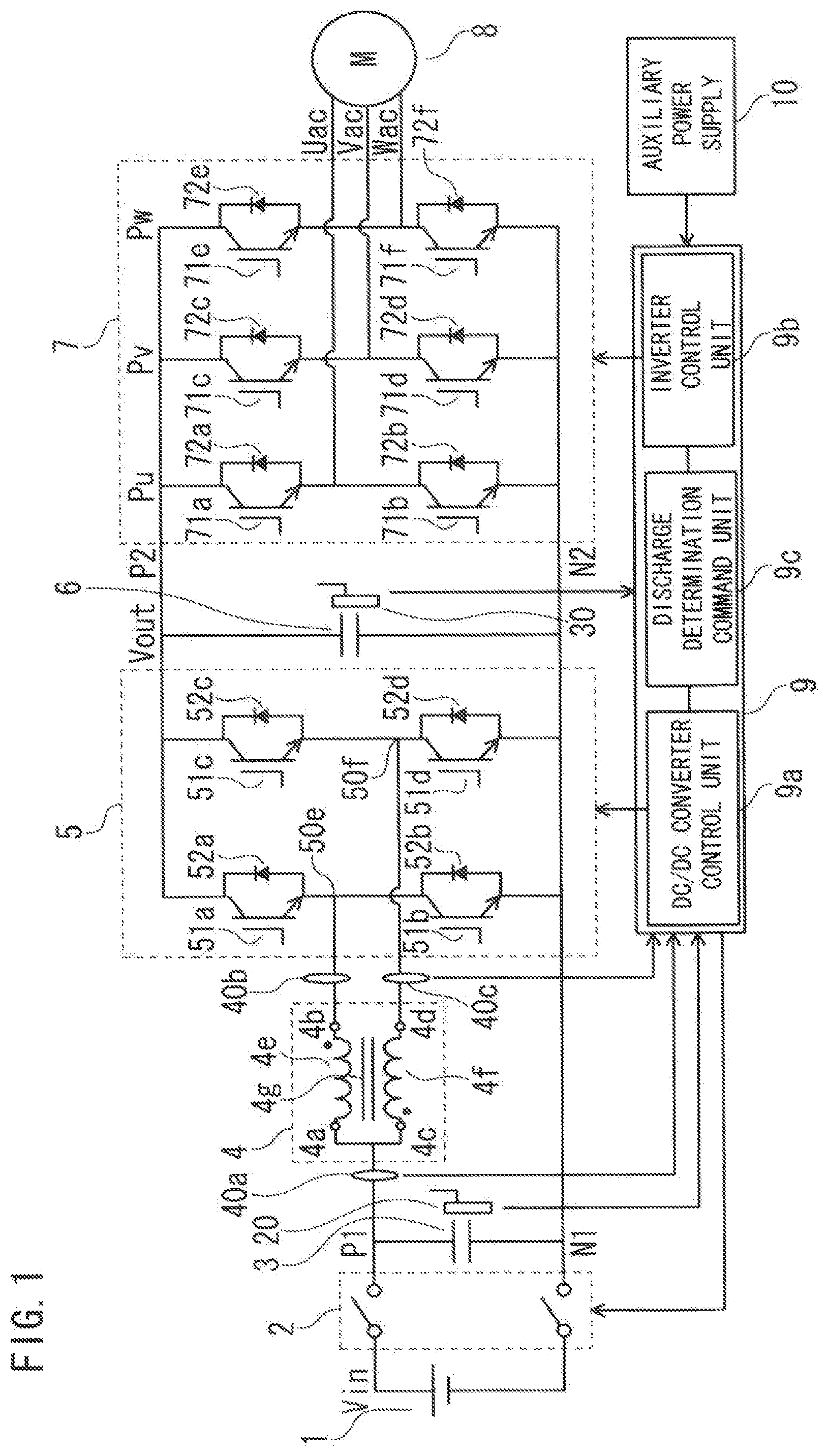
The present disclosure relates to a power conversion device mounted on an electric vehicle, for example. Conventionally, there has been known an electric vehicle including a DC power supply capable of charging and discharging, a boost converter for boosting DC voltage supplied from the DC power supply, a first smoothing capacitor for smoothing voltage between the DC power supply and the boost converter, an inverter for converting high DC voltage outputted from the boost converter to AC voltage, a second smoothing capacitor for smoothing voltage between the boost converter and the inverter, and a three-phase AC electric motor to which the AC voltage outputted from the inverter is applied, whereby a driving force and a braking force of the vehicle are controlled. In such an electric vehicle, in order to ensure safety of the vehicle, it is necessary to immediately discharge high-voltage electric charge stored in a smoothing capacitor when the vehicle collides or power is stopped, thereby preventing electric shock. In addition, it is required that the capacity of a backup power supply serving as an operation power supply for performing discharge control of the boost converter so as to shorten the discharge period is reduced to downsize the power conversion device. Therefore, conventionally, technologies as described in, for example, Patent Documents 1 and 2 below have been proposed. An electric vehicle described in Patent Document 1 includes two bidirectional DC/DC converters, and capacitors are connected to a low-voltage end and a high-voltage end of the two bidirectional DC/DC converters. During traveling, a control device supplies drive pulse signals in which ON timings are shifted from each other and in which OFF timings are shifted from each other, to semiconductor switching elements of the bidirectional DC/DC converters. Meanwhile, at the time of discharging the capacitors, drive pulse signals having matched ON timings and matched OFF timings are supplied to the semiconductor switching elements of the bidirectional DC/DC converters in order to shorten the discharge period. In a conventional method of discharging by alternately turning on and off upper and lower arms of an inverter, when the arms composing the inverter are short-circuited, discharging cannot be performed due to overcurrent or the like. In this regard, in a power conversion device described in Patent Document 2, a DC/DC converter having four arms connected in series is used, occurrence of arm short-circuit is detected, and electric charges stored in input and output capacitors are discharged via a coupled reactor and the DC/DC converter. Patent Document 1: Japanese Laid-Open Patent Publication No. 2017-85696 Patent Document 2: Japanese Laid-Open Patent Publication No. 2015-33153 However, in both conventional technologies described in Patent Documents 1 and 2, currents flowing through the coupled reactor are triangular wave currents having a switching frequency, and the current components thereof contain only a switching frequency component of the DC/DC converter. Therefore, copper loss in current conduction is small, and thus an effect of consuming energy of the capacitors is small, so that it takes time to perform discharging. In addition, the power supply capacity of the backup power supply serving as an operation power supply for performing discharge control of the DC/DC converter so as to shorten the discharge period is still great. The present disclosure has been made to solve the above problem, and an object of the present disclosure is to provide a power conversion device in which a pair of coupled reactors of a coupling type magnetically coupled are provided at an input stage of a DC/DC converter, and which enables the discharge period of capacitors to be shortened according to operation of the DC/DC converter in comparison with the conventional case, and which enables size reduction of a backup power supply for driving the DC/DC converter for discharge control. A power conversion device according to the present disclosure includes: a coupled reactor magnetically coupled and a DC/DC converter for voltage conversion, which are provided between a DC power supply and an inverter for driving an electric motor; a first smoothing capacitor connected between the DC power supply and the coupled reactor; a second smoothing capacitor connected between the DC/DC converter and the inverter; a switch for turning on/off the DC power supply, the switch being interposed between the first smoothing capacitor and the DC power supply; and a controller configured to control switching operations of semiconductor switching elements included in the inverter and the DC/DC converter. The DC/DC converter has a full-bridge configuration in which two legs are connected in parallel, each leg being formed by connecting, in series, a pair of upper and lower arms having the semiconductor switching elements. The coupled reactor includes a first winding and a second winding each having one end side connected to a positive side of the DC power supply. The first winding has another end side connected to a connection point between the upper and lower arms composing a first leg of the legs. The second winding has another end side connected to a connection point between the upper and lower arms composing a second leg of the legs. The controller unit, in accordance with a discharge command, opens the switch, causes the semiconductor switching elements composing the upper and lower arms of the DC/DC converter to perform complementary operations so as to be alternately turned on/off, and causes the pair of legs to operate with their switching phases shifted from each other. EFFECT OF THE INVENTION According to a power conversion device of the present disclosure, circulating current can flow through a DC/DC converter and a coupled reactor between a first smoothing capacitor and a second smoothing capacitor, whereby electric charges stored in the first smoothing capacitor and the second smoothing capacitor can be immediately discharged by copper loss occurring in a path through which current flows, iron loss occurring in the core of the coupled reactor, and loss occurring in the DC/DC converter. Thus, the discharge period of the first smoothing capacitor and the second smoothing capacitor can be shortened in comparison with the conventional case, and accordingly, the backup power supply for driving the DC/DC converter for discharge control can be downsized. In the case of using a differential-type coupled reactor in which DC magnetic fluxes are generated in such directions as to cancel out each other when DC current flows, a current component that is a multiple of the frequency is generated in the conduction current, whereby copper loss can be increased. In the case of using a cumulative-type coupled reactor in which DC magnetic fluxes are generated in such directions as to strengthen each other when DC current flows, the conduction current is made to be reflux current and thus have a square-wave shape, whereby the current effective value is increased and thus copper loss in the coupled reactor can be increased. In The DC power supply 1 is capable of charging and discharging, and transmits/receives power to/from the electric motor 8 via the inverter 7. The DC/DC converter 5 is provided between the DC power supply 1 and the inverter 7, and boosts DC voltage supplied from the DC power supply 1. The first smoothing capacitor 3 is connected between the DC power supply 1 and the DC/DC converter 5, and smooths voltage between the DC power supply 1 and the DC/DC converter 5. The first voltage sensor 20 measures voltage between a high-voltage node and a low-voltage node of the first smoothing capacitor 3. A current sensor 40 The inverter 7 converts high DC voltage outputted from the DC/DC converter 5, to AC voltage, by DC/AC conversion. The second smoothing capacitor 6 is connected between the DC/DC converter 5 and the inverter 7, and smooths voltage between the DC/DC converter 5 and the inverter 7. The second voltage sensor 30 measures voltage between a high-voltage node and a low-voltage node of the second smoothing capacitor 6. AC voltage outputted from the inverter 7 is applied to the electric motor 8, whereby a driving force and a braking force for the vehicle are controlled. During driving of the vehicle, the switch 2 is closed in order to connect the DC power supply 1, to the first smoothing capacitor 3 and the DC/DC converter 5. When usage of the vehicle is finished and stoppage of power is detected, or when collision of the vehicle is detected by an acceleration sensor (not shown) or the like, the switch 2 is opened in order to disconnect the DC power supply 1 from the DC/DC converter 5, the first smoothing capacitor 3 and the differential-type coupled reactor 4. The controller 9 includes a DC/DC converter control unit 9 The DC/DC converter control unit 9 Regarding the power semiconductor elements in the DC/DC converter 5, a unit in which each semiconductor switching element 51 Here, the configuration of the DC/DC converter 5 will be described in detail. The DC/DC converter 5 is a full-bridge type in which four semiconductor switching elements 51 Next, the detailed configuration of the inverter 7 will be described. In the inverter 7, legs the number of which corresponds to the number of phases of the electric motor to be driven are provided. As shown in The inverter control unit 9 Next, with reference to Here, the coupled reactor is formed by a core 4 One end side 4 The upper and lower arms of the DC/DC converter 5, which are connected to the differential-type coupled reactor 4, are complementarily operated so as to be alternately turned on/off, and also, the legs are operated such that their phases are shifted from each other to alternately excite the first winding 4 Here, the slopes of current ripples occurring in the differential-type coupled reactor 4 will be shown using mathematical expressions. The voltage across the first winding 4 When the self-inductances of the first winding 4 The current i1 and the current i2 are composed of the current component i1 When the current i1 and the current i2 are summed, as shown by the following (Expression 5), the circulation current components (ilac) are canceled out. Thus a slope that is a multiple of the current component (ildc) caused due to the non-circulating magnetic flux component in each winding is obtained. From (Expression 1) to (Expression 4), the current components i1 The input voltage to the differential-type coupled reactor 4 is denoted by Vin, and the output voltage of the DC/DC converter 5 is denoted by Vout. Table 1 shows the voltage across the coupled reactor 4, which changes depending on the switching states of the semiconductor switching elements 51 By substituting the above voltage into (Expression 6) and (Expression 7), it is possible to calculate the slope of current that changes according to the switching states. Next, in the case of normal driving of the vehicle, i.e., normal power conversion operation in which, while the switch 2 is turned on, the two legs of the DC/DC converter 5 are alternately operated with their phases shifted from each other to alternately excite the first winding 4 In Regarding operation modes, four modes of state (T1), state (T2), state (T3), and state (T4) are sequentially repeated in accordance with the operation states of the semiconductor switching elements 51 [A] First, as shown in (1) During the period in state (T1), the semiconductor switching element 51 At this time, the first winding 4 In the second winding 4 Here, for simplification of the description, it is assumed that the slope of the current component occurring due to a circulating magnetic flux is 4, and the slope of the current component occurring due to a non-circulating magnetic flux is 6. Using this numerical value example, changes in the waveforms of current ripples occurring in the first winding 4 During this period, the slope of the current i1 (2) During the period in state (T2), the semiconductor switching element 51 This period is a period in which excitation of the first winding 4 (3) During the period in state (T3), the semiconductor switching element 51 At this time, the first winding 4 In the second winding 4 At this time, magnetic coupling is made such that the magnetic flux from the second winding 4 (4) During the period in state (T4), as well as in the case of state (T2), the semiconductor switching element 51 This period is a period in which excitation of the first winding 4 As described above, in the case of D<0.5, regarding the first winding 4 [B] Next, as shown in (1) During the period in state (T1), the semiconductor switching element 51 During this period, in the first winding 4 Therefore, during this period, as well as in the above case of D<0.5, it is assumed that the slope of current i1 (2) During the period in state (T2), the semiconductor switching element 51 During this period, a circulating magnetic flux occurs in the first winding 4 (3) During the period in state (T3), the semiconductor switching element 51 (4) During the period in state (T4), the semiconductor switching element 51 During this period, a circulating magnetic flux occurs in the first winding 4 As described above, in the case of D>0.5, regarding the first winding 4 In order that the current components may include a large amount of current component that is a multiple of the switching frequency of switching of the DC/DC converter 5, it is necessary that, in the case of D<0.5, the following (Expression 8) is satisfied during the period in state (T3), and in the case of D>0.5, the following (Expression 9) is satisfied during the period in state (T2). Using (Expression 6), (Expression 7), and Table 1, the relational expressions of (Expression 8) and (Expression 9) are arranged by using L (self-inductance), M (mutual inductance), and D (duty ratio). As a result, the following (Expression 10) and (Expression 11) are obtained. Case of D<0.5 Case of D>0.5 Under the condition in which the above relational expressions are satisfied, When the lower arm is operated with the condition of D>0.5 using the DC/DC converter 5 so as to discharge the first smoothing capacitor 3 and the second smoothing capacitor 6, As described above, it is found that currents i1, i2 containing frequency components that are a multiple of the switching frequency of switching of the semiconductor switching elements in the DC/DC converter 5 flow through the first winding 4 Next, when collision of the vehicle is detected or when usage of the vehicle is finished and stoppage of power is detected, a discharge operation in which the semiconductor switching elements 51 When collision of the vehicle is detected or when usage of the vehicle is finished and stoppage of power is detected, the switch 2 is turned off, the inverter 7 is stopped by the inverter control unit 9 In this case, the control operation of the DC/DC converter control unit 9 However, in the discharge operation in this case, the switching frequency of the DC/DC converter 5 is lowered in comparison with the case of normal power conversion operation, so that current ripple increases within an allowable current range in the DC/DC converter 5. Thus, loss increases, whereby the discharge period in the case where the switch 2 is turned off can be shortened. When such a discharge operation is performed, LC resonance occurs in the first smoothing capacitor 3, the second smoothing capacitor 6, and the differential-type coupled reactor 4. Therefore, if the switching frequency of the DC/DC converter 5 is excessively lowered, there is a possibility that resonance voltage and resonance current that exceed the allowable values of the DC/DC converter 5, the first smoothing capacitor 3, and the second smoothing capacitor 6, occur. Accordingly, as shown in If the discharge period of the first smoothing capacitor 3 and the second smoothing capacitor 6 is shortened as described above, the power supply capacity of the auxiliary power supply 10 for supplying power to the controller 9 which performs drive control of the DC/DC converter 5 for performing discharge operation can be reduced, whereby the entire power conversion device can be downsized. A power conversion device according to embodiment 2 of the present disclosure is characterized in that the coupling configuration of the coupled reactor 4 used in embodiment 1 is changed to a cumulative type. The other configurations are the same as the configurations in embodiment 1, and therefore the detailed description thereof is omitted. Here, the cumulative-type coupled reactor 4 refers to a coupled reactor in which the first winding 4 When the DC/DC converter 5 is driven by phase shift operation using the cumulative-type coupled reactor 4, the DC/DC converter 5 performs reflux operation, as shown in Although the disclosure is described above in terms of various exemplary embodiments and implementations, it should be understood that the various features, aspects, and functionality described in one or more of the individual embodiments are not limited in their applicability to the particular embodiment with which they are described, but instead can be applied, alone or in various combinations to one or more of the embodiments of the disclosure. It is therefore understood that numerous modifications which have not been exemplified can be devised without departing from the scope of the present disclosure. For example, at least one of the constituent components may be modified, added, or eliminated. At least one of the constituent components mentioned in at least one of the preferred embodiments may be selected and combined with the constituent components mentioned in another preferred embodiment. 1 DC power supply 2 switch 3 first smoothing capacitor 4 coupled reactor 4 4 4 40 5 DC/DC converter 51 6 second smoothing capacitor 7 inverter 71 8 electric motor 9 controller 9 9 9 10 auxiliary power supply 20 first voltage sensor 30 second voltage sensor A magnetically coupled reactor and a DC/DC converter are provided between a DC power supply and an inverter. A first smoothing capacitor is provided between the DC power supply and the coupled reactor. A second smoothing capacitor is provided between the DC/DC converter and the inverter. A controller is provided in order to control switching operations of the inverter and the DC/DC converter. The controller causes semiconductor switching elements composing upper and lower arms of the DC/DC converter to perform complementary operations so as to be alternately turned on/off, and causes left and right legs to operate with their switching phases shifted from each other, thereby electric charges stored in both smoothing capacitors are discharged by energy loss in the coupled reactor and the DC/DC converter. 1. A power conversion device comprising:
a coupled reactor magnetically coupled and a DC/DC converter for voltage conversion, which are provided between a DC power supply and an inverter for driving an electric motor; a first smoothing capacitor connected between the DC power supply and the coupled reactor; a second smoothing capacitor connected between the DC/DC converter and the inverter; a switch for turning on/off the DC power supply, the switch being interposed between the first smoothing capacitor and the DC power supply; and a controller configured to control switching operations of semiconductor switching elements included in the inverter and the DC/DC converter, wherein the DC/DC converter has a full-bridge configuration in which two legs are connected in parallel, each leg being formed by connecting, in series, a pair of upper and lower arms having the semiconductor switching elements, the coupled reactor includes a first winding and a second winding each having one end side connected to a positive side of the DC power supply, the first winding has another end side connected to a connection point between the upper and lower arms composing a first leg of the legs, the second winding has another end side connected to a connection point between the upper and lower arms composing a second leg of the legs, and the controller, in accordance with a discharge command, opens the switch, causes the semiconductor switching elements composing the upper and lower arms of the DC/DC converter to perform complementary operations so as to be alternately turned on/off, and causes the pair of legs to operate with their switching phases shifted from each other, whereby the first smoothing capacitor and the second smoothing capacitor are discharged. 2. The power conversion device according to the controller controls the DC/DC converter so that AC current circulates through the coupled reactor and the DC/DC converter between the first smoothing capacitor and the second smoothing capacitor and electric charges stored in the first smoothing capacitor and the second smoothing capacitor are discharged by energy loss due to the coupled reactor and the DC/DC converter. 3. The power conversion device according to the coupled reactor is a differential type in which DC magnetic fluxes generated by the first winding and the second winding are formed in such directions as to cancel out each other when DC current flows through the first winding and the second winding. 4. The power conversion device according to AC current containing a component that is a multiple of a switching frequency of the DC/DC converter flows through the coupled reactor by setting so as to satisfy the following relationships: in a case of D<0.5, M/L>D/(1-D) in a case of D>0.5, M/L>(1-D)/D where D is a duty ratio with which the semiconductor switching elements of the DC/DC converter are turned on/off, L is a self-inductance of the coupled reactor, and M is a mutual inductance of the coupled reactor. 5. The power conversion device according to when the switch is turned off, the controller changes the duty ratio with which the semiconductor switching elements of the DC/DC converter are turned on/off, in accordance with voltages of the first smoothing capacitor and the second smoothing capacitor or a voltage difference therebetween, so as to maximize ripple current flowing through the coupled reactor within such a range as not to exceed a certain allowable value set in advance. 6. The power conversion device according to the coupled reactor is a cumulative-type in which DC magnetic fluxes generated by the first winding and the second winding are generated in such directions as to strengthen each other when DC current flows through the first winding and the second winding. 7. The power conversion device according to when the switch is turned off, the controller shifts a phase of the DC/DC converter in accordance with voltages of the first smoothing capacitor and the second smoothing capacitor or a voltage difference therebetween, so as to maximize ripple current flowing through the coupled reactor within such a range as not to exceed a certain allowable value set in advance. 8. The power conversion device according to when the switch is turned off, the controller causes the semiconductor switching elements of the DC/DC converter to operate at a switching frequency lower than that in a case where the switch is turned on, so that the first smoothing capacitor and the second smoothing capacitor are discharged by energy loss due to the coupled reactor and the DC/DC converter. 9. The power conversion device according to the controller performs control so that the switching frequency for the semiconductor switching elements in the case where the switch is turned off is gradually lowered with elapse of time, whereby a current peak during discharging is reduced. 10. The power conversion device according to 11. The power conversion device according to the coupled reactor is a differential type in which DC magnetic fluxes generated by the first winding and the second winding are formed in such directions as to cancel out each other when DC current flows through the first winding and the second winding. 12. The power conversion device according to AC current containing a component that is a multiple of a switching frequency of the DC/DC converter flows through the coupled reactor by setting so as to satisfy the following relationships: in a case of D<0.5, M/L>D/(1-D) in a case of D>0.5, M/L>(1-D)/D where D is a duty ratio with which the semiconductor switching elements of the DC/DC converter are turned on/off, L is a self-inductance of the coupled reactor, and M is a mutual inductance of the coupled reactor. 13. The power conversion device according to when the switch is turned off, the controller changes the duty ratio with which the semiconductor switching elements of the DC/DC converter are turned on/off, in accordance with voltages of the first smoothing capacitor and the second smoothing capacitor or a voltage difference therebetween, so as to maximize ripple current flowing through the coupled reactor within such a range as not to exceed a certain allowable value set in advance. 14. The power conversion device according to the coupled reactor is a cumulative-type in which DC magnetic fluxes generated by the first winding and the second winding are generated in such directions as to strengthen each other when DC current flows through the first winding and the second winding. 15. The power conversion device according to when the switch is turned off, the controller shifts a phase of the DC/DC converter in accordance with voltages of the first smoothing capacitor and the second smoothing capacitor or a voltage difference therebetween, so as to maximize ripple current flowing through the coupled reactor within such a range as not to exceed a certain allowable value set in advance.TECHNICAL FIELD
BACKGROUND ART
CITATION LIST
Patent Document
SUMMARY OF THE INVENTION
Problems to be Solved by the Invention
Means of Solution to the Problems
BRIEF DESCRIPTION OF THE DRAWINGS
EMBODIMENTS FOR CARRYING OUT THE INVENTION
Embodiment 1
Voltage across reactor depending on switching states 51b 51d V1e V2e V1e + V2e V1e − V2e ON OFF Vin Vin − Vout 2Vin − Vout Vout OFF ON Vin − Vout Vin 2Vin − Vout −Vout ON ON Vin Vin 2Vin 0 OFF OFF Vin − Vout Vin − Vout 2Vin − 2Vout 0 Embodiment 2
DESCRIPTION OF THE REFERENCE CHARACTERS