반도체 발광소자
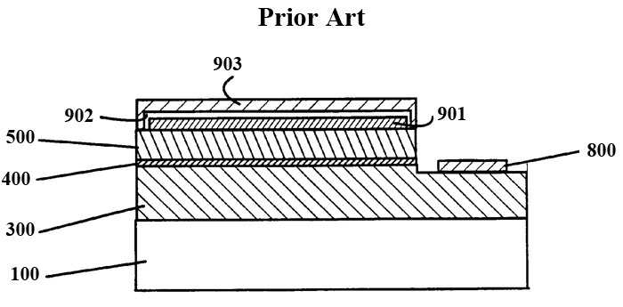
The present disclosure (Disclosure) consists in its entirety of semiconductor light-emitting device relates to, in particular current path due to a difference between currents, which are that are to carry, and prevent durability from relates to a semiconductor light emitting element. Wherein, semiconductor light-emitting device electron and hole mobilities that a light mixture by the addition of an initiator semiconductor optical device, to nitride semiconductor light emitting element wherein group 3 may. 3 nitride a semiconductor (x) Ga (y) Al In (1-X-Y) N (0 ≤ x ≤ 1, 0 ≤ y ≤ 1, 0 ≤ x + y ≤ 1) comprising an oxygenic compound is is.. Used in red-luminous addition GaAs-based semiconductor light emitting element and the like to may. Here, the present disclosure is provided to background art are ball number, these necessarily mean all is not publicly known technique (This section provides background information related to the present disclosure which is not necessarily prior art). Figure 1 shows a call 7,262,436 disclosure also American Patent Registration Notification number one example of a compound semiconductor light emitting device are as drawing representing a, semiconductor light-emitting device comprises a substrate (100), substrate (100) on which a layer of snow grown grown on n-type semiconductor layer (300), n-type semiconductor layer (300) grown on an active layer (400), active layer (400) grown on a p-type semiconductor layer (500), p-type semiconductor layer (500) formed on the reflective film that functions in a electrode (901,902,903) and etching the exposed n style layer (300) provided on the bonding pad side n (800) includes. One end of the chip, i.e. the substrate, (100) on one side of the electrode (901,902,903) and electrode (800) both there is formed a, electrode (901,902,903) is reflective film that functions in a type chip is (filp chip) sees the same. Electrode (901,902,903) an electrode of high reflectance (901; e.g.: Ag), bonding, and electrode (903; e.g.: Au) the electrodes and (901) and (903) an electrode prevents diffusion of between the (902; e.g.: Ni) be at 500. Such metal can realize high reflectance in a range structure, current spreading is advantageous but, by the metal and the has a drawback in that as a light-absorbing. Figure 2 shows a call also Japanese Public Patent Notification number 2006 - 20913 disclosure one example of a compound semiconductor light emitting device are as drawing representing a, semiconductor light-emitting device comprises a substrate (100), substrate (100) grown on a buffer layer (200), buffer layer (200) grown on a n-type semiconductor layer (300), n-type semiconductor layer (300) grown on an active layer (400), active layer (400) grown on a p-type semiconductor layer (500), p-type semiconductor layer (500) a dielectric layer is formed over the, current spreading serving the function of translucent conductive film (600), translucent conductive film (600) provided on the bonding pad side p (999 0000181999) and etching the exposed n style layer (300) provided on the bonding pad side n (800) includes. And translucent conductive film (600) on the distributed Bragg reflector (900; DBR: Distributed Bragg Reflector) and the metal reflective film (904) is having. Matched way when, metal (904) a light-absorbing by but reducing the, electrode (901,902,903) relatively rather than using current spreading to prevent the excessive force and abrasion. and a fixed. Call 6,307,218 Patent Registration Notification number American also Figure 3 shows a disclosure of an electrode structure that is as representing a one example, is forming spacer light-emitting device (for example, transverse/longitudinal is 1000um/1000um) according to, bonding pad side p (700) which acts as a bonding pad side n and a n-side electrode (800) having a spacing corresponding to that of the to provided to achieve an enhanced electrode an, improved current spreading light which, for accurately, with sufficient current supply addition to bonding pad side p (700) and a n-side electrode (800) are each two, and are provided. Plurality of (710,810) and a plurality to a bonding pad of but is, their introduction light emitting surface of the process chamber is brought or the like for reducing luminous efficiency includes disfunction. The 'of the invention embodiment for a content' at time t2. on the succeeding stage of the. Here, the present disclosure is the overall abstract (Summary) are ball number, this number periphery of the of the present disclosure a only is understood. is not but (This section provides a general summary of the disclosure and is not a comprehensive disclosure of its full scope or all of its features). The present disclosure according to with one aspect (According to one aspect of the present disclosure), semiconductor light emitting device, a conductive semiconductor layer number 1 number 1, number 1 number 2 other to the conductivity type of the semiconductor layer a conductive number 2, number 1 and number 2 semiconductor layer is interposed between the semiconductor layer and a contact for generating light by a plurality of semiconductor layers having active layer; stimulated between the electrons and the holes one of semiconductor layer number 1 number 1 electrode portion and, other of the stimulated between the electrons and the holes semiconductor layer number 2 number 2 electrode portion; and a dielectric layer is formed over the plurality of semiconductor layers, active layer reflects light from an insulating reflective layer; includes, number 1 electrode portion and number 2 electrode part are formed on the entire: coupled to a top electrode being formed on reflective layer insulating; insulating reflective layer under plurality semiconductor layer in electrical communication with one islands (island type) ohmic electrode, provate exchange system having funcation of internal ohmic electrode, provate exchange system having funcation of internal ohmic electrode extends from an electrode; and insulating reflective layer through the epitaxial channel adjustment layer, a ripeness of kimchi and an upper electrode ohmic electrode provate exchange system having funcation of internal electrical connection a Kla test device; includes, the ohmic electrode provate exchange system having funcation of internal ohmic electrode island-shape it is area than a semiconductor light-emitting device having is ball number. The present disclosure according to of the other of aspect (According to another aspect of the present disclosure), semiconductor light emitting device, a conductive semiconductor layer number 1 number 1, number 1 number 2 other to the conductivity type of the semiconductor layer a conductive number 2, number 1 and number 2 semiconductor layer is interposed between the semiconductor layer and a contact for generating light by a plurality of semiconductor layers having active layer; stimulated between the electrons and the holes one of semiconductor layer number 1 number 1 electrode portion and, other of the stimulated between the electrons and the holes semiconductor layer number 2 number 2 electrode portion; and a dielectric layer is formed over the plurality of semiconductor layers, active layer reflects light from an insulating reflective layer; includes, number 1 electrode portion and number 2 electrode part are formed on the entire: coupled to a top electrode being formed on reflective layer insulating; insulating reflective layer under plurality semiconductor layer in electrical communication with one a provate exchange system having funcation of internal ohmic electrode, and of twisting a handset's cord in ohmic electrode extends from an electrode; insulating reflective layer through the epitaxial channel adjustment layer provate exchange system having funcation of internal ohmic and an upper electrode connecting the connection electrodes and liver ohmic electrode provate exchange system having funcation of internal and 99900003269 99 of the portion where a followed, provate exchange system having funcation of internal ohmic electrode and the branch electrodes for reinforcement; characterized in that including a semiconductor light-emitting device having is ball number. The 'of the invention embodiment for a content' at time t2. on the succeeding stage of the. Figure 1 shows a call 7,262,436 disclosure also American Patent Registration Notification number one example of a compound semiconductor light emitting device are representing a surface, Figure 2 shows a call also Japanese Public Patent Notification number 2006 - 20913 disclosure a compound semiconductor light emitting device are one example of representing a surface, Figure 3 shows a disclosure also American Patent Registration Notification number 6,307,218 call indicative of one example of an electrode structure that is surface, Figure 4 shows a disclosure according to one example of semiconductor light-emitting device a are also representing a surface, Figure 5 shows a also in Figure 4 a single cross section cutting along the line one example of that describes a surface, Also 6 and Figure 7 shows a semiconductor light emitting element are also a disclosure according to one example of method bath number account for facets, Figure 8 shows a a are also in another example of a semiconductor light-emitting device disclosure according to account for one side, Figure 9 shows a a are also a second example of a programmable semiconductor light emitting disclosure according to account for one side, Figure 10 shows a a are also a second example of a programmable semiconductor light emitting disclosure according to account for one side, Figure 11 shows a a are also a second example of a programmable semiconductor light emitting disclosure according to account for one side. Hereinafter, the present disclosure with reference to a drawing with an a described the antennae (The present disclosure will now be described in detail with reference to the accompanying drawing (s)). Figure 4 shows a a are also representing the disclosure according to one example of semiconductor light-emitting device and drawing, Figure 5 in Figure 4 a single line cutting along the cross section is one example of that describes a surface. Semiconductor light-emitting device comprises a plurality of semiconductor layers (30, 40, 50), number 1 electrode portion (80, 81, 82, 84, 85), number 2 electrode portion (70, 71, 72, 74, 75), and insulating reflective layer (R) includes. Plurality of semiconductor layers (30, 40, 50) a conductive number 1 the number 1 semiconductor layer (30), a conductive number 2 number 1 number 2 other to the conductivity type of the semiconductor layer (50), and number 1 semiconductor layer (30) and number 2 semiconductor layer (50) between a drain region are formed at both and a contact for generating light by an active layer (40) includes. Number 1 electrode portion (80, 81, 82, 84, 85) the number 1 semiconductor layer (30) electrically and which are in communication between the electrons and the holes tank and one, number 2 electrode portion (70, 71, 72, 74, 75) the number 2 semiconductor layer (50) electrically and which are in communication between the electrons and the holes is supplied to and the other one of the nozzle. Insulating reflective layer (R) the plurality of semiconductor layers (30, 40, 50) a dielectric layer is formed over the, active layer (40), and reflects light from.. The present disclosure number 2 electrode portion and number 1 in an insulating electrode part are formed on the entire reflective layer (R) coupled to a top electrode being formed on, island-shape (island type) ohmic electrode, provate exchange system having funcation of internal ohmic electrode, the branch electrodes, electrical connection includes electrical connection and additional. Island-ohmic electrode, provate exchange system having funcation of internal ohmic electrode, electrodes and liver under an insulating reflective layer (R) plurality of semiconductor layers (30, 40, 50) in electrical communication with one and.. Island-shape (island type) a circular, triangle, generally, such as of polygonal such as rectangular extends long in the one side (extending). shape that is not. The branch electrodes the provate exchange system having funcation of internal constitution: extends from ohmic electrode. Reflective layer an insulating electrical connection (R) through the between the first and an upper electrode ohmic provate exchange system having funcation of internal, additional electrical connection an insulating reflective layer (R) through the connects the and an upper electrode ohmic island-shape. The ohmic electrode provate exchange system having funcation of internal greater not electrically ohmic electrode island-shape. In present semiconductor light-emitting device comprises a upper electrode (80, 70) to the insulating reflective layer (R) based on the plurality of semiconductor layers (30, 40, 50) opposite the side of the is a flip chip (flip chip). In present, number 1 electrode portion (80, 81, 82, 84, 85) the number 1 upper electrode (80), etching the exposed semiconductor layer number 1 (30) on island-shape ohmic electrode number 1 (82), number 1 provate exchange system having funcation of internal ohmic electrode (84), and number 1 provate exchange system having funcation of internal ohmic electrode (84) extending from the branch electrodes number 1 (85) includes. Number 2 electrode portion (70, 71, 72, 74, 75) the number 2 upper electrode (70), number 2 semiconductor layer (50) dielectric reflective layer (R) between the ohmic electrode island-shape number 2 (72), ohmic electrode provate exchange system having funcation of internal number 2 (74), and number 2 provate exchange system having funcation of internal ohmic electrode (74) extending from the branch electrodes number 2 (75) includes. Island-ohmic electrode (82, 72) and provate exchange system having funcation of internal ohmic electrode (84, 74) both upper electrode (80, 70) are each coupled to since, theoretically number 1 electrode portion (80, 81, 82, 84, 85) the etc. dislocation and, number 2 electrode portion (70, 71, 72, 74, 75) also loop but, provate exchange system having funcation of internal ohmic electrode (84, 74) electrodes a liver - (85, 75) is connected and, thereby provate exchange system having funcation of internal ohmic electrode (84, 74) electrodes and liver (85, 75) is coupled contour (outline) contains at least one conditions of the current flow or island-shape ohmic electrode (82, 72) and. the difference that. Island-shape thereby ohmic electrode (82, 72) rather than ohmic electrode provate exchange system having funcation of internal (84, 74) upon by an electric current with the more or, a cold water valve is of current flows through both or more threshold may be proposed. When a long operation this case, provate exchange system having funcation of internal ohmic electrode (84, 74) durability in. is installed. Such door operating in high-current has number a semiconductor light-emitting device is number door further expanded in their. The present in ohmic electrode island-shape (82, 72) than ohmic electrode provate exchange system having funcation of internal (84, 74) larger area of, provate exchange system having funcation of internal ohmic electrode (84, 74) the fluid can flow into the current limitations of increased and the, semiconductor light-emitting device is protected from damage or breakage endurance was a stirring wing number door. Hereinafter, 3 - port orthogonally polarized MIMO antenna for example the described. Plurality of semiconductor layers (30, 40, 50) a substrate (10) a dielectric layer is formed over the, substrate (10) mainly at sapphire, SiC, Si, GaN is is used as the, substrate (10) may be for producing a sedated number final decision is going to be. Number 1 semiconductor layer (30) and number 2 semiconductor layer (50) can be its position changes with the, in - port orthogonally polarized MIMO antenna 3 mainly GaN be at 500. Plurality of semiconductor layers (30, 40, 50) a substrate (10) formed on the buffer layer (20), a conductive number 1 number 1 semiconductor layer (30; e.g.: Si doped GaN), a conductive number 2 number 1 number 2 other to the conductivity type of the semiconductor layer (50; e.g.: Mg doped GaN) and number 1 semiconductor layer (30) and number 2 semiconductor layer (50) between a drain region are formed at both light stimulated between the electrons and the holes generating layer (40; e.g.: (In) InGaN/GaN multiple quantum well structure) includes. Plurality of semiconductor layers (30, 40, 50) may comprise multilayer each, buffer layer (20) can be dispensed with. Preferably number 2 semiconductor layer (50) on current spreading conductive film (60; e.g.: ITO, Ni/Au) top elid processing device is provided with. Insulating reflective layer (R) the current spreading conductive film (60), number 1 the branch electrodes (85), and number 2 the branch electrodes (75) is diffusion barrier layer formed to cover a, active layer (40) light from substrate (10) the side. Insulating reflective layer (R) in present metal reflection the light-absorbing layer for reducing the stator is formed of a insulating material, preferably (Distributed Bragg Reflector) or DBR (omni-directional Reflector) including of ODR can be multilayer structure. For example, as number 5 to it became at the time of also, insulating reflective layer (R) sequential stacked dielectric film (91b), DBR (91a), and the clad just (91c) may include a. Upper electrode number 1 (80) and number 2 upper electrode (70) an insulating reflective layer (R) spaced from one another, on upper electrode number 1 (80) of edge and number 2 upper electrode (70) is having edge of opposite to each other. Upper electrode number 1 (80) and number 2 upper electrode (70) communicating with the external directly joined or, wire bonding may be. Number 1 the branch electrodes (85) the number 2 upper electrode (70) and extends below, number 2 the branch electrodes (75) the upper electrode number 1 (80) has extends below. Island-shape ohmic electrode number 1 (82) the number 2 upper electrode (70) facing the upper electrode number 1 (80) from an edge of a provate exchange system having funcation of internal ohmic electrode number 1 (84) away than the first, number 2 ohmic electrode island-shape (72) the upper electrode number 1 (80) facing the upper electrode number 2 (70) from an edge of a number 2 provate exchange system having funcation of internal ohmic electrode (74). be far apart, than. Island-shape and ohmic electrode (82, 72) for positioning the leads the branch electrodes (85, 75) extending in a-pressing method so as to protect elements.. The present in number 1 the branch electrodes (85) number 1 on prolongation of ohmic electrode island-shape (82) is, number 2 the branch electrodes (75) number 2 on prolongation of island-shape ohmic electrode (72), but is, island-ohmic electrode (82, 72) such position of extension line. may be outside of on. In present, plurality of number 1 the branch electrodes (85) is number 2 semiconductor layer (50) and active layer (40) exposed is etched semiconductor layer number 1 (30) is having thereon, each number 1 the branch electrodes (85) each number 1 provate exchange system having funcation of internal ohmic electrode (84) extends from. Electrical connection (81) an insulating reflective layer (R) through the upper electrode number 1 (80) and provate exchange system having funcation of internal ohmic electrode number 1 (84) connects the. Other electrical connection (81) an insulating reflective layer (R) through the upper electrode number 1 (80) and island-shape ohmic electrode number 1 (82) connects the. Island-shape ohmic electrode number 1 (82) and number 1 provate exchange system having funcation of internal ohmic electrode (84) the number 1 semiconductor layer (30) and in electrical connection with at (81) and reducing a contact resistance between the stability of, and transfer, thus enhancing durabilitycopyright 2000. Number 2 ohmic electrode island-shape (72), number 2 provate exchange system having funcation of internal ohmic electrode (74), and number 2 the branch electrodes (75) the current spreading conductive film (60) dielectric reflective layer (R), which are installed on the between, the present in plurality of number 2 the branch electrodes (75) a plurality of number 1 the branch electrodes (85) approximately parallel at high provided with a, number 2 ohmic electrode island-shape (72) the number 2 the branch electrodes (75) which is situated on the prolongation of.. Each number 2 the branch electrodes (75) each number 2 provate exchange system having funcation of internal ohmic electrode (74) extends from. Electrical connection (71) an insulating reflective layer (R) number 2 through the upper electrode (70) and number 2 provate exchange system having funcation of internal ohmic electrode (74) connects the. Other electrical connection (71) an insulating reflective layer (R) number 2 through the upper electrode (70) and number 2 ohmic electrode island-shape (72) connects the. Number 2 ohmic electrode island-shape (72) and number 2 provate exchange system having funcation of internal ohmic electrode (74) the current spreading conductive film (60) and in electrical connection with at (71) between the and reducing a contact resistance, and transfer of. increase the stability. Preferably, light absorbing film (41) is number 2 semiconductor layer (50) and current spreading conductive film (60) between the number 2 the branch electrodes (75), ohmic electrode island-shape number 2 (72), and number 2 provate exchange system having funcation of internal ohmic electrode (74) respectively corresponding to can be than. Light absorbing film (41) theSiO2, TiO2can be, and the like, active layer (40) some or all of the light emitted from the reflecting only functions leads to a better and even when they have a, number 2 the branch electrodes (75), number 2 ohmic electrode island-shape (72), and number 2 provate exchange system having funcation of internal ohmic electrode (74) and prevent current flow under from only functions to good even when they have a, preferably even when they have a port through both. The branch electrodes (85, 75) and ohmic electrode (82, 84, 72, 74) a plurality of metal layer may be, number 1 semiconductor layer (30) or current spreading conductive film (60) particularly in its excellent contact contact layer, such as a layer reflection mirror the light reflection characteristic will and can comprise of. The present e.g. according to semiconductor light-emitting device comprises a metal reflective layer insulating instead (R) also using flip chip than it became at the time of number 1 to light-absorbing by the metal and the. cell-based compositions effective in the loss reduction. In addition, emitting surface substantially insulating reflective layer (R) is between the substrate and, island-ohmic electrode (82, 72), of twisting a handset's cord in ohmic electrode (84, 74), electrodes and liver (85, 75) using current flow or passage is relatively more and position of number of a input device in the in, also 2 to cell-based compositions effective in the current spreading than flip chip it became at the time of number.. Thus island-ohmic electrode (82, 72), of twisting a handset's cord in ohmic electrode (84, 74), electrodes and liver (85, 75) in a structure having, current supply of uniformity or, ohmic electrode island-shape for second sustain electrodes (82, 72), of twisting a handset's cord in ohmic electrode (84, 74), electrodes and liver (85, 75) properly the detection position or the number, and shape can be altered by means of 2000. An advantageous such a purpose in a composite structure is ohmic electrode island-shape (82, 72) than ohmic electrode provate exchange system having funcation of internal (84, 74) upon by an electric current with the relative to further rectilinear number door durability is protected from damage or breakage when. it is possible to eliminate the. Rated current as well as when the, does not desired high current can flow which directly comes into contact, provate exchange system having funcation of internal ohmic electrode (84, 74) island-shape current the leaning even ohmic electrode (82, 72) of area greater than sufficiently, so damages to. have a certain durability. Island-shape ohmic electrode number 1 (82) and provate exchange system having funcation of internal ohmic electrode number 1 (84) the ratio of area of, number 2 ohmic electrode island-shape (72) and number 2 provate exchange system having funcation of internal ohmic electrode (74) of a current is a ratio of a first ohmic electrode provate exchange system having funcation of internal (84, 74) according to a degree of further rectilinear direction determined by to fall within an appropriate range can be. On the other hand, number 1 provate exchange system having funcation of internal ohmic electrode (84) and number 2 provate exchange system having funcation of internal ohmic electrode (74) have the property of to flow current to and can be other than the, thus, number 1 provate exchange system having funcation of internal ohmic electrode (84) and number 2 provate exchange system having funcation of internal ohmic electrode (74) saves luminance can be removed except. For example, number 1 usually provate exchange system having funcation of internal ohmic electrode (84) number 2 than provate exchange system having funcation of internal ohmic electrode (74) upon by an electric current with the rectilinear may be worse have the property of, in this case, provate exchange system having funcation of internal ohmic electrode number 1 (84) number 2 than provate exchange system having funcation of internal ohmic electrode (74) produces a large area of can be a in the embodiment is taken into consideration when calibration. Also 6 and Figure 7 shows a semiconductor light emitting element are also a disclosure according to one example of method bath number account for as drawing, with a 7 also to 4 also, first, 5 and 6 to also as it became at the time of number, substrate (10) on semiconductor layer number 1 (30), active layer (40), number 2 semiconductor layer (50) is formed, light absorbing film (41) is formed, current spreading thereon conductive film (60; e.g.: ITO) is formed, mesa etched number 1 semi layer (30) part of (35) a is exposed. Mesa etch current spreading conductive film (60) may be carried out before the forming. Current spreading conductive film (60) can be dispensed with. After, also as it became at the time of number to 7, number 1 exposed semiconductor layer (30) and current spreading conductive film (60) on the branch electrodes (85, 75), and ohmic electrode (82, 84, 72, 74) is formed on. After, current spreading conductive film (60) on insulating reflective layer (R) is formed on. Insulating reflective layer (R) in present metal reflection the light-absorbing layer for reducing the stator is formed of a insulating material, preferably (Distributed Bragg Reflector) or DBR (omni-directional Reflector) including of ODR can be multilayer structure. For example, dielectric film (91b), distributed Bragg reflector (91a) and the cladding film (91c) is formed the insulating reflective layer (R) is formed. Dielectric film (91b) or clad film (91c) can be dispensed with. Distributed Bragg reflector (91a) the, for example, SiO2and aTiO2is arranged on a pair of plurality of times. In addition distributed Bragg reflector (91a) theTa2O5, HfO, ZrO, SiNequal and a high refractive index material such as with low refractive index dielectric thin film (which are representative of aSiO2)can be such as to a bottom of the. Insulating reflective layer (R) m several is its thickness (e.g.: 1 - 8 micro m) can be degree. After, insulating reflective layer (R) method such as dry etching when the and forms sheds in the row -, connected to through an opening (81, 71) is formed on. Insulating reflective layer (R) and an upper electrode (80, 70) is formed on. Electrical connection (81, 71) and an upper electrode (70, 80) but can be a separate, in the course of one may be integrally formed. Figure 8 shows a a are also in another example of a semiconductor light-emitting device disclosure according to account for as drawing, light absorbing prevention film constitution: cigar omitted. Island-ohmic electrode (82, 72) compared to ohmic electrode provate exchange system having funcation of internal (84, 74) of electric current to a further lean preention according to damage a semiconductor light-emitting device can be number the door, electrode or contour (outline) urgent pipe coupling edge of angle narrow or in particular is a portion of a door can be is number. On the other hand, as a metal electrode part light absorbent so that the branch electrodes (85, 75) or ohmic electrode (82, 84, 72, 74) includes a plurality surface of a limitation of.. The present e.g. ohmic electrode island-shape semiconductor emitting device according to (82, 72) and provate exchange system having funcation of internal ohmic electrode (84, 74) which bonding pads surface of, the aforementioned durability or once the presence of a damaged door number provate exchange system having funcation of internal ohmic electrode in order to solve (84, 74) electrodes and liver (85, 75) of the portion where a followed, ohmic electrode and the branch electrodes (85, 75) for reinforcement (77, 87) has a. Reinforcement in Figure 8 (77, 87) the provate exchange system having funcation of internal ohmic electrode (84, 74) electrodes and liver (85, 75) is divided into a dotted lines, they may be formed as integrated together. Reinforcement (77, 87), in the case of no, provate exchange system having funcation of internal ohmic electrode (84, 74) electrodes and liver (85, 75) is coupled or pipe coupling urgent in contour (outline) edge of narrow angle (e.g.: 79) is formed, turns on the high current driving in durability or instantaneous flow of high current the good do not go. Reinforcement (77, 87) edge of the such a small angle (79) inhibit formation of. In addition, reinforcement (77, 87) the provate exchange system having funcation of internal ohmic electrode (84, 74) integrally increased KIPO & is protruded from the guide area. As a result, said door and for circuit controlling isolation gates of generation number number ., grease. In present reinforcement (77, 87) the branch electrodes (85, 75) whose width is reduced which an LCD panel, reinforcement (77, 87) and a provate exchange system having funcation of internal ohmic electrode (84, 74) electrodes and liver (85, 75) is coupled by applying spherically washing water or at a narrow angle piece and is installed in a extend the branch electrodes (85, 75) which is inclined at an angle of with a tilt extended.. Reinforcement (77, 87) the electromigration phenomenon is not the shape of the. deformed. Figure 9 shows a a are also a second example of a programmable semiconductor light emitting disclosure according to account for as, provate exchange system having funcation of internal ohmic electrode (84, 74) the island-shape ohmic electrode (82, 72) than area is large, provate exchange system having funcation of internal ohmic electrode (84, 74) electrodes and liver (85, 75) to the connection part of reinforcement (77, 87) is integrally formed at a part of.. Thus, . durability. Reinforcement (77, 87) and a provate exchange system having funcation of internal ohmic electrode (84, 74), electrodes and liver (85, 75) by applying spherically washing water pipe coupling extend in straight curve or soft without, said by applying spherically a trumpet-shaped (horn or trumpet type) is relatively narrow which the branch electrodes (85, 75) extending in.. In present, provate exchange system having funcation of internal ohmic electrode (84, 74) the contour of the branch electrodes based on the electrical connections thereto (85, 75) is the photo engraving opposite side of, reinforcement (77, 87) by applying spherically can be semi-circular, that is at a tangent. Figure 10 shows a a are also a second example of a programmable semiconductor light emitting disclosure according to account for as drawing, provate exchange system having funcation of internal ohmic electrode (84, 74) electrodes and liver (85, 75) to the connection part of reinforcement (77, 87) to, number 9 to slightly differently e.g. it became at the time of is formed convex. Each of twisting a handset's cord in ohmic electrode (84, 74) each island-shape area of ohmic electrode (82, 86, 72, 76) which larger than those of, plurality of island-ohmic electrode (82, 86, 72, 76) surface of. different. Plurality of island-ohmic electrode (82, 86, 72, 76) degree position, of the rotary drum when which differs from that of current is according to, can be have an area different each other. In present, provate exchange system having funcation of internal ohmic electrode (84, 74) clock, which is approximate to the island-shape ohmic electrode (82, 72) is far ohmic electrode island-shape (86, 76) is larger but not electrically, and area may be is provided. Figure 11 shows a a are also a second example of a programmable semiconductor light emitting disclosure according to account for as, provate exchange system having funcation of internal ohmic electrode (84, 74) the island-shape ohmic electrode (82, 72) than area is large, provate exchange system having funcation of internal ohmic electrode (84, 74) electrodes and liver (85, 75) is subsequently formed reinforcement a portion (77, 87) is integrally formed at a part of.. The branch electrodes (85, 75) has a width of a constant extensions and, is extending than the expansion section (88, 78) includes. As such, the branch electrodes (85, 75) the a width varies according to position be a constant or a is mounted between rotating plates coupled to example, straight the branch electrodes as well as curved includes even in the case of the branch electrodes. Hereinafter the present disclosure of a variety of embodiment relates to form. (1) semiconductor light emitting device, a conductive semiconductor layer number 1 number 1, number 1 number 2 other to the conductivity type of the semiconductor layer a conductive number 2, number 1 and number 2 semiconductor layer is interposed between the semiconductor layer and a contact for generating light by a plurality of semiconductor layers having active layer; stimulated between the electrons and the holes one of semiconductor layer number 1 number 1 electrode portion and, other of the stimulated between the electrons and the holes semiconductor layer number 2 number 2 electrode portion; and a dielectric layer is formed over the plurality of semiconductor layers, active layer reflects light from an insulating reflective layer; includes, number 1 electrode portion and number 2 electrode part are formed on the entire: coupled to a top electrode being formed on reflective layer insulating; insulating reflective layer under plurality semiconductor layer in electrical communication with one islands (island type) ohmic electrode, provate exchange system having funcation of internal ohmic electrode, and of twisting a handset's cord in ohmic electrode extends from an electrode; and insulating reflective layer through the epitaxial channel adjustment layer [...] connected and an upper electrode ohmic provate exchange system having funcation of internal electrical connection (an electrical connection); includes, the ohmic electrode provate exchange system having funcation of internal ohmic electrode island-shape it is area than a semiconductor light-emitting device. (2) electrodes and liver ohmic electrode provate exchange system having funcation of internal of the portion where a followed provate exchange system having funcation of internal ohmic electrode and the branch electrodes for reinforcement; a characterized in including a semiconductor light-emitting device. (3) from a top view, the branch electrodes have a top electrode outer surface of the measurement pipe extending in a, a liver - ohmic electrode island-shape electrodes side upper electrode from an edge of a a remote than ohmic electrode provate exchange system having funcation of internal characterized in a semiconductor light-emitting device. (4) provate exchange system having funcation of internal ohmic electrode, reinforcement, and liver the contour of electrodes (outline) of the curve of which and is provided as a either a semiconductor light-emitting device characterized in. (5) island-shape island-shape further area and ohmic electrode ohmic electrode; for characterized in including a semiconductor light-emitting device. (6) number 1 which the switching element is arranged and: upper electrode number 1; and number 2 semiconductor layer and the activation layers exposed ohmic electrode island-shape semiconductor layer a number 1 number 1, number 1 provate exchange system having funcation of internal ohmic electrode, and number 1 the branch electrodes; includes, number 2 which the switching element is arranged and: upper electrode number 2; and between insulating semiconductor layer number 2 ohmic electrode island-shape number 2, number 2 provate exchange system having funcation of internal ohmic electrode, and includes electrodes is number 2, the branch electrodes number 1 number 2 and extends below upper electrode, the branch electrodes number 2 which extends below upper electrode number 1, number 1 number 1 number 1 electrode side is the ohmic electrode island-shape upper electrode from an edge of the first away than ohmic electrode provate exchange system having funcation of internal number 1, number 2 is the ohmic electrode island-shape number 2 number 2 from an edge of a upper electrode number 2 electrode side ohmic electrode provate exchange system having funcation of internal characterized in be far apart, than a semiconductor light-emitting device. (7) in semiconductor light-emitting device, a conductive semiconductor layer number 1 number 1, number 1 number 2 other to the conductivity type of the semiconductor layer a conductive number 2, number 1 and number 2 semiconductor layer is interposed between the semiconductor layer and a contact for generating light by a plurality of semiconductor layers having active layer; stimulated between the electrons and the holes one of semiconductor layer number 1 number 1 electrode portion and, other of the stimulated between the electrons and the holes semiconductor layer number 2 number 2 electrode portion; and a dielectric layer is formed over the plurality of semiconductor layers, active layer reflects light from an insulating reflective layer; includes, number 1 electrode portion and number 2 electrode part are formed on the entire: coupled to a top electrode being formed on reflective layer insulating; insulating reflective layer under plurality semiconductor layer in electrical communication with one a provate exchange system having funcation of internal ohmic electrode, and of twisting a handset's cord in ohmic electrode extends from an electrode; insulating reflective layer through the epitaxial channel adjustment layer provate exchange system having funcation of internal ohmic and an upper electrode connecting the connection; electrodes and liver ohmic electrode the substrate is attached to the other of the portion where a followed provate exchange system having funcation of internal ohmic electrode and the branch electrodes for reinforcement; a characterized in including a semiconductor light-emitting device. (8) facing away from the feed end the branch electrodes ohmic electrode and provate exchange system having funcation of internal plurality semiconductor layer in electrical communication with one a island-ohmic electrode; and insulating reflective layer through the epitaxial channel adjustment layer connected and an upper electrode ohmic island-shape in addition to a second electrical connection; includes, the ohmic electrode provate exchange system having funcation of internal ohmic electrode island-shape it is area than a semiconductor light-emitting device. (9) provate exchange system having funcation of internal ohmic electrode, reinforcement, and liver (outline) electrodes being free from ardor the contour of a curved and is provided as a at least one characterized in a semiconductor light-emitting device. (10) the branch electrodes the; extended portion constant width; and lock is coupled the expansion section is it sees extension; a characterized in including a semiconductor light-emitting device. The present disclosure according to semiconductor light emitting one selected from a, based on variations in that the electric current flowing through the current path number in a door, . durability of semiconductor light-emitting device. In addition, light-absorbing by the metal and the losses are reduced. Number 1 semiconductor layer (30), active layer (40), number 2 semiconductor layer (50), (80) upper electrode number 1 Island-shape ohmic electrode number 1 (82), number 1 provate exchange system having funcation of internal ohmic electrode (84), (85) number 1 the branch electrodes Reinforcement (87, 77), number 2 upper electrode (70), number 2 ohmic electrode island-shape (72), Number 2 provate exchange system having funcation of internal ohmic electrode (74), number 2 the branch electrodes (75) Disclosed is a semiconductor light emitting device. The semiconductor light emitting device includes: a plurality of semiconductor layers having a first semiconductor layer, a second semiconductor layer, and an active layer; a first electrode part for supplying one of an electron and a hole to the first semiconductor layer, and a second electrode part for supplying the other of the electron and the hole to the second semiconductor layer; and an insulating reflection layer formed on the multiple semiconductor layers, for reflecting light emitted from the active layer, wherein at least one of the first electrode part and the second electrode part includes: an upper electrode formed on the insulating reflection layer; an island type ohmic electrode, a connection type ohmic electrode, and a branch electrode branched out from the connection type ohmic electrode to electrically communicate with the multiple semiconductor layers under the insulating reflection layer; and an electrical connection which connects the connection ohmic electrode to the upper electrode by passing through the insulating reflection layer. An area of the connection type ohmic electrode is larger than an area of the island type ohmic electrode. Semiconductor light emitting device, a conductive semiconductor layer number 1 number 1, number 1 number 2 other to the conductivity type of the semiconductor layer a conductive number 2, number 1 and number 2 semiconductor layer is interposed between the semiconductor layer and a contact for generating light by a plurality of semiconductor layers having active layer; stimulated between the electrons and the holes one of semiconductor layer number 1 number 1 electrode portion and, other of the stimulated between the electrons and the holes semiconductor layer number 2 number 2 electrode portion; so, the condensed water a dielectric layer is formed over the semiconductor layer, active layer reflects light from an insulating reflective layer; includes, number 1 electrode portion and number 2 electrode part are formed on the entire: coupled to a top electrode being formed on reflective layer insulating; insulating reflective layer under plurality semiconductor layer in electrical communication with one islands (island type) ohmic electrode, provate exchange system having funcation of internal ohmic electrode, and of twisting a handset's cord in ohmic electrode extends from an electrode; so lofty virtues ductility provate exchange system having funcation of internal reflective layer through the epitaxial channel adjustment layer island-shape ohmic electrode and ohmic and an upper electrode connecting the connection (an electrical connection); includes, the ohmic electrode provate exchange system having funcation of internal ohmic electrode island-shape it is area than a semiconductor light-emitting device. According to Claim 1, ohmic electrode and liver provate exchange system having funcation of internal electrodes of the portion where a followed provate exchange system having funcation of internal ohmic electrode and the branch electrodes for reinforcement; a characterized in including a semiconductor light-emitting device. According to Claim 1, from a top view, the branch electrodes have a top electrode outer surface of the measurement pipe extending in a, a liver - ohmic electrode island-shape electrodes side upper electrode from an edge of a a remote than ohmic electrode provate exchange system having funcation of internal characterized in a semiconductor light-emitting device. According to Claim 2, provate exchange system having funcation of internal ohmic electrode, reinforcement, and liver the contour of electrodes (outline) of the curve of which and is provided as a either a semiconductor light-emitting device characterized in. According to Claim 1, island-shape island-shape further area and ohmic electrode ohmic electrode; for characterized in including a semiconductor light-emitting device. According to Claim 1, number 1 which the switching element is arranged and: upper electrode number 1; and number 2 semiconductor layer and the activation layers exposed ohmic electrode island-shape semiconductor layer a number 1 number 1, number 1 provate exchange system having funcation of internal ohmic electrode, and number 1 the branch electrodes; includes, number 2 which the switching element is arranged and: upper electrode number 2; and between insulating semiconductor layer number 2 ohmic electrode island-shape number 2, number 2 provate exchange system having funcation of internal ohmic electrode, and includes electrodes is number 2, the branch electrodes number 1 number 2 and extends below upper electrode, the branch electrodes number 2 which extends below upper electrode number 1, number 1 number 1 number 1 electrode side is the ohmic electrode island-shape upper electrode from an edge of the first away than ohmic electrode provate exchange system having funcation of internal number 1, number 2 is the ohmic electrode island-shape number 2 number 2 from an edge of a upper electrode number 2 electrode side ohmic electrode provate exchange system having funcation of internal characterized in be far apart, than a semiconductor light-emitting device. Number ablation Number ablation Number ablation Number ablation