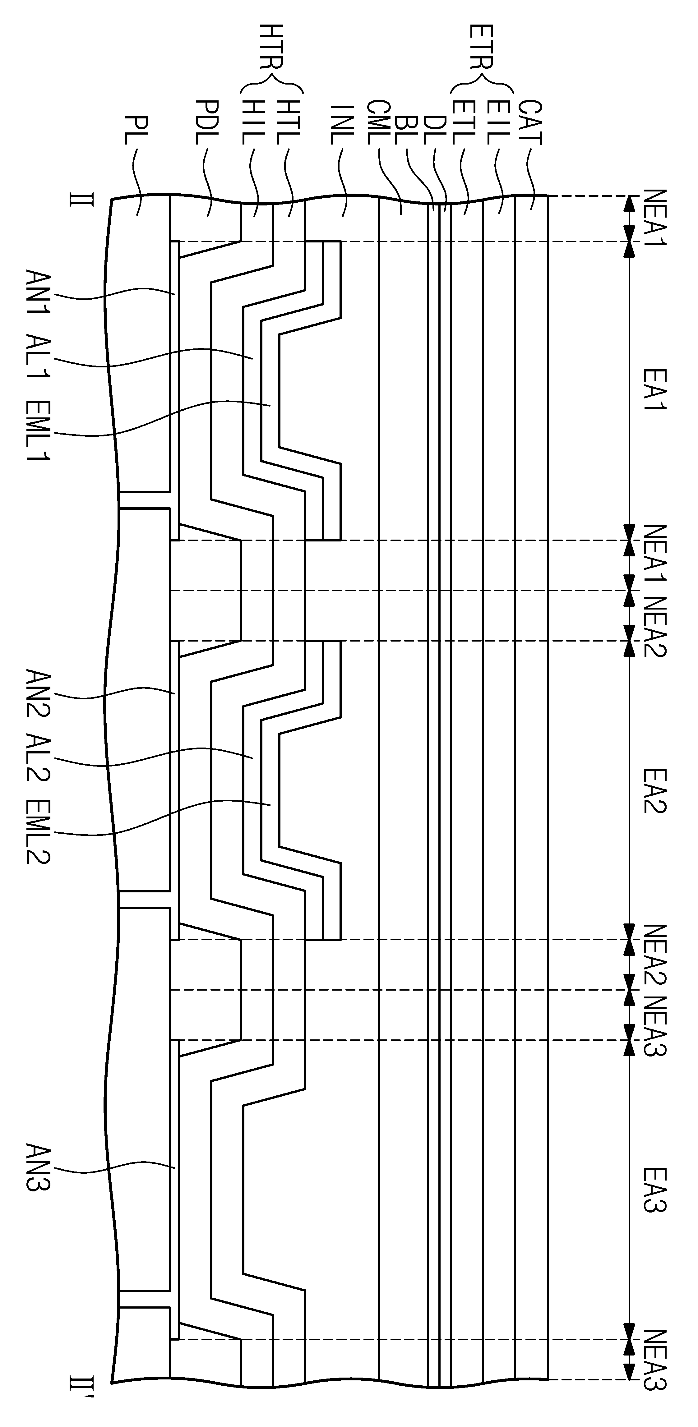
ORGANIC LIGHT-EMITTING DEVICE AND DISPLAY APPARATUS INCLUDING SAME
The present invention refers to organic light emitting element and display device including the same are disclosed. The light receiving type flat panel display device (flat display device) is classification sport can. -emitting include flat cathode ray tube and (flat cathode ray tube), plasma display panel (plasma display panel) and, organic light emitting display device (organic light emitting display, OLED) etc.. Said organic light emitting display device is an organic light emitting device without using a tool. Said organic light emitting device is a light emitting element and display device as, a wide visual field angle, excellent contrast, etc. certain sizes of response speed. The, or organic light emitting display device includes a digital camera, or video camera, or camcorder, or a portable information terminal, or smart phone, notebook or the first and, tablet personal computer, such as for mobile device display device or flexible display device, be applied to a large-area electronic number in elevator apparatus such as an electrical large number etc. to penetrate through a shaped article or article. Organic light emitting device comprises a light-emitting layer emit light is recombined in anode and the electrons injected comprised of color principles to implement, and the electrons injected from the base state (exciton) it is herein obtained by combining the OLEDs emitting substrate. The purpose of the invention long life photosensitive organic light emitting under public affairs number are disclosed. The purpose of the invention is a high efficiency and long life under public affairs number display device are disclosed. One of the present invention first and second light-emitting element prepared in the embodiment according to number 1, number 2 number 3 prepared sub organic light emitting element and the other module. An upper element said number 1 prepared anode number 1, number 1 light emitting layer, a light-emitting unit common number 1, buffer unit number 1, number 1 comprising 701,702,703 doped portions and number 1. An upper element said number 2 prepared anode number 2, number 2 light emitting layer, a light-emitting unit common number 2, number 2 buffer unit, comprising doped portions and number 2 701,702,703 number 2. Said number 3 prepared an upper element number 3 anode, common light emitting unit number 3, number 3 buffer unit, comprising doped portions number 3 and number 3 701,702,703. Said number 1 common light emitting unit, a light-emitting unit and said number 3 are disclosed with the first common common light emitting said number 2. Said number 1 buffer unit, said number 2 buffer with the first buffer unit and said number 3 are disclosed. Said number 1 doped portions, said number 2 doped portions and said number 3 doped portions are integrated disclosed. Collided said number 1, said number 2 it digs up and cow [tu[tu] it blows collided and said number 3 is integrated. 620 nm to 750 nm polarized light spot of said number 1 the light emitting layer, said number 2 the light emitting layer of 495 nm to 570 nm polarized light spot, said number 1 common light emitting unit, said number 2 440 nm to 490 nm of wavelength band from the light emitting unit and said number 3 common common a current may be disclosed. A light emitting layer between the anode and said number 1 which said number 1 prepared element said number 1 number ball number 1 further includes hole transport regions, said number 2 prepared element said number 2 number 2 which further includes light emitting layer between the anode and said number 2 number ball hole transport regions, said number 3 prepared anode and said number 3 number 3 hole transport regions between which said number 3 element emitting unit further includes common ball number, said number 1 hole transport regions, said number 2 hole transport regions and said number 3 can be a hole transport regions are integrated. Said number 1 prepared element number 1 further including light emitting layer between said number 1 hole transport regions and said number 1 number which may be auxiliary hole. Said number 2 prepared hole transport regions and said number 2 number 2 number between said number 2 element further including light emitting layer which may be auxiliary hole. Said number 1 prepared element number 1 further includes electron transport regions doped portions said number 1 on which ball number, said number 2 prepared element further includes electron transport regions doped portions said number 2 number 2 on which ball number, said number 3 prepared element number 3 further includes electron transport regions doped portions said number 3 on which ball number, said number 1 electron transport regions, said number 2 electron transport regions and said number 3 can be a electron transport regions are integrated. Said number 1 prepared element, said number 2 sub organic light emitting element and said number 3 prepared element can be a target ball number are distanced from each other. In the embodiment according to one of the present invention display device includes a base substrate, a light emitting layer number 1, number 2 light emitting layer, common light emitting layer, buffer layer and comprise a doped layer. Said number 1 the alignment part aligns said light emitting region, said number 2 light emitting region and said number 3 emitting region with each other. Said number 1 the light emitting layer from the light emitting said number 1 disposed thereon. Said number 2 the light emitting layer from the light emitting said number 2 disposed thereon. Said light emitting region common light-emitting layer said number 1, said number 2 light-emitting region located light emitting region and said number 3, light-emitting layer and a light emitting layer on said number 1 and number with said number 2 ball are disclosed. Said buffer layer is a light-emitting region said number 1, said number 2 light-emitting region located light emitting region and said number 3, and number on said common light emitting layer integrated ball are disclosed. Said at least one n-type dopant doped layers and, said number 1 light-emitting region, said number 2 located light emitting region and said number 3 light-emitting region, and said buffer layer on integrated ball number are disclosed. The gate number ball and said common light-emitting layer said base substrate, said buffer layer is on the gate number ball and said common light emitting layer, said buffer layer on said doped layers the gate number can be a target ball. Said number 1 of 620 nm to 750 nm light-emitting region is polarized light spot, said number 2 of 495 nm to 570 nm light-emitting region is polarized light spot, said number 3 of 440 nm to 490 nm light-emitting region is a wavelength band from the light source may be disclosed. 620 nm to 750 nm polarized light spot of said number 1 the light emitting layer, said number 2 the light emitting layer of 495 nm to 570 nm polarized light spot, said common light-emitting layer 440 nm to 490 nm wavelength band of the light source may be disclosed. In the embodiment according to display device of the present invention includes a light emitting region in said number 1, said number 2 located light emitting region and said number 3 light-emitting region, said common light emitting layer between the base substrate and said ball and number, further comprises a hole transporting region can be integral. In the embodiment according to display device of the present invention includes one light emitting said number 1 are located in regions, said hole transport region and said number 1 further includes a light emitting layer which can be ball number between the auxiliary layer number 1. In the embodiment according to display device of the present invention includes one light emitting said number 2 are located in regions, said hole transport region and said number 2 which further includes a light emitting layer between the auxiliary layer number 2 can be ball number. Said hole transport region is said number on the base substrate on which said hole transporting layer including number ball hole injection layer and which ball hole injection layer may be disclosed. In the embodiment according to display device of the present invention includes a light emitting region in said number 1, said number 2 light-emitting region located light emitting region and said number 3, and ball number on said doped layer, further including integral electron transporters may be disclosed. Said electron transport region on which said electron transport layer and electron transport layer on said doped layer number hole injection layer improved drain hole number including may be disclosed. The organic light emitting device in the embodiment according to one of the present invention, which can enhance the efficiency, can extend the service life. In the embodiment according to the display device of the present invention one, which can enhance the efficiency, can extend the service life. In the embodiment according to Figure 1 shows a cross-section of the present invention also visually representing one to determine the organic light-emitting device are disclosed. In the embodiment according to Figure 2 shows a cross-section of the present invention also visually representing one to determine the organic light-emitting device are disclosed. In the embodiment according to Figure 3 shows a display device of the present invention indicating one to determine sensors mounted thereon also are disclosed. Figure 4 shows a display device of the present invention also included one in the embodiment according to one of the pixel circuit are disclosed. Figure 5 shows a display device of the present invention also included one in the embodiment according to information indicating one of a plane sub pixels are disclosed. Figure 6 shows a I a-I ' cross-sectional drawing of Figure 5 indicating determine the LCD panel assembly displays are disclosed. Figure 7 shows a schematic diagram of the display device of the present invention also included one in the embodiment according to generally flat sub pixels are disclosed. Figure 8 shows a iI a-iI ' cross-sectional drawing of Figure 7 indicating determine the LCD panel assembly displays are disclosed. Figure 9 shows a iI a-iI ' cross-sectional drawing of Figure 7 indicating determine the LCD panel assembly displays are disclosed. Or more the purpose of the invention are, are other purposes, features and advantages of the attached drawing will easily understand associated with over the preferred embodiment hereinafter. However the present invention refers to the other in the embodiment described herein are not limited to are embodied in the form disapproval. Rather, the disclosure are introduced in the embodiment wherein the intimate intermixing of the contents of the present invention can be complete and for allowing relative to conventional ball number which can be transmitted in order to sufficiently to event are disclosed. Each drawing are described as well as a component while similar references in a similar. In the attached drawing, the dimensions of the structures of the present invention can be higher than for clarity thread number series are disclosed. Number 1, number 2 describes various components such as term can be used but, in terms of said components are defined by said back like. Components are mounted to one of said terms are used only distinguished from other components of the object. For example, number 1 number 2 outside of the range of the present invention rights without components can be termed components, similarly number 2 of the elements can be termed component number 1. It is apparent that a single representation of the differently in order not providing language translators, comprising plurality of representation. In the application, the term "comprising" or "having disclosed" specification of articles feature, number, step, operation, components, parts or specify a combination not present included, another aspect of one or more moveable number, step, operation, component, piece or a combination of pre-times the number should not understood to presence or additional possibility. In addition, layer, film, region, such as when that plate parts which are "on", "directly on" as well as any other portion when intermediate when another portion comprises a unit. On the contrary layer, film, region, such as when that plate parts which are "lower", "beneath" as well as any other portion when intermediate when another portion comprises a unit. The organic light emitting device in the embodiment according to one of the present invention hereinafter is described substrate. In the embodiment according to Figure 1 shows a cross-section of the present invention also visually representing one to determine the organic light-emitting device are disclosed. In the embodiment according to Figure 2 shows a cross-section of the present invention also visually representing one to determine the organic light-emitting device are disclosed. The reference 2 also 1 and also, in the embodiment according to organic light-emitting device of the present invention is organic light emitting device (S_OEL1) (OEL) one sub number 1, number 2 and number 3 (S_OEL2) organic light-emitting device comprising the light-emitting element prepared sub (S_OEL3). Organic light emitting device (S_OEL1) sub number 1, number 2 and number 3 prepared element includes a light-emitting device prepared (S_OEL2) (S_OEL3) number 1 (DR1) spaced from one ball number encoded in cross direction. Number 1 620 nm to 750 nm and emits the polarized light of the light-emitting element prepared (S_OEL1). The light source includes a red light emitting element (S_OEL1) number 1 prepared may be disclosed. (S_OEL1) number 1 (DR1) which intersects the direction is number 1 prepared element number 2 (DR2) direction sequentially stacked anode (AN1) number 1, number 1 (EML1) light-emitting layer, a light-emitting unit (CMPL1) common number 1, number 1 (BLP1) buffer unit, number 1 and number 1 (CATP1) doped portions (DLP1) comprising the collided. Number 2 (S_OEL2) 495 nm to 570 nm and emits the polarized light of the light-emitting device prepared. The light source comprises a green light emitting element (S_OEL2) number 2 prepared may be disclosed. (S_OEL2) direction (DR2) number 2 number 2 prepared element is sequentially stacked anode (AN2) number 2, number 2 (EML2) light-emitting layer, a light-emitting unit (CMPL2) common number 2, number 2 (BLP2) buffer unit, number 2 and number 2 (CATP2) collided doped portions (DLP2) without using a tool. (S_OEL3) is 440 nm to 490 nm of number 3 prepared element emits polarized light is reflected. The light source comprises a blue light emitting element (S_OEL3) number 3 prepared may be disclosed. (S_OEL3) direction (DR2) number 3 prepared element is sequentially stacked anode (AN3) number 3 number 2, number 3 (CMPL3) common light emitting unit, the buffer unit (BLP3) number 3, number 3 and number 3 (CATP3) collided doped portions (DLP3) without using a tool. Anode (AN1) number 1, number 2 and number 3 anode (AN2) anode (AN3) spaced apart from each other in cross section is encoded ball number. Anode (AN1) number 1, number 2 and number 3 number 1 (DR1) anode (AN2) anode (AN3) is encoded number hole spaced from one direction. Anode (AN1) number 1, number 2 and number 3 anode (AN2) anode (AN3) is transmission electrodes, transflective electrode or be a reflective electrode. Anode (AN1) number 1, number 2 and number 3 anode (AN2) anode (AN3) if each transmission electrodes, anode (AN1) number 1, number 2 and number 3 each anode (AN2) anode (AN3) transparent metal oxide, e.g., ITO (indium tin oxide), IZO (indium zinc oxide), ZnO (zinc oxide), ITZO (indium tin zinc oxide) can be consists of. Anode (AN1) number 1, number 2 and number 3 each transflective electrode or anode (AN2) reflective electrode when the anode (AN3), anode (AN1) number 1, number 2 and number 3 each anode (AN2) anode (AN3) Ag, Mg, Al, Pt, Pd, Au, Ni, Nd, Ir, or can be a mixture of Cr. Anode (AN1) number 1, number 2 and number 3 on the hole transporting region (HTR) anode (AN2) anode (AN3) encoded ball number. The hole injection layer (HIL) (HTR) hole transporting region comprises electron transporting layer (HTL). Hole injection layer (HIL) electron transporting layer (HTL) can be formed into one layer may be filled. But that does not itself shown, hole transport region (HTR) stop layer further comprises at least one of the hole buffer layer and can be. The hole injection layer (HIL) (copper phthalocyanine) phthalocyanine compounds such as copper phthalocyanine (phthalocyanine); DNTPD (N, n' non-diphenyl-a n, n' a-bis - [4 - (phenyl m tolyl-a product) - phenyl] - biphenyl-a '4,4 non-diamine), the m-mTDATA (4, 4', 4 "- tris (3 a-methylphenylphenylamino) triphenylamine), TDATA (4, 4 '4" - Tris (N, n-a diphenylamino) triphenylamine), 2 TNATA (4, 4', 4" - tris {N, - (2 a-naphthyl) - n-a phenylamino} - triphenylamine), PEDOT/PSS (Poly (3,4 provided ethylenedioxythiophene)/Poly (4 a-styrenesulfonate), PANI/DBSA (Polyaniline/Dodecylbenzenesulfonic acid), PANI/CSA (Polyaniline/Camphor sulfonicacid), PANI/PSS ((Polyaniline)/Poly (4 a-styrenesulfonate) but the like, limited to are not correct. Hole injection layer (HIL) for the conductivity enhancer can be further includes a charge generation material. Hole injection layer (HIL) charge generation material is uniformly dispersed within or non-uniformly dispersed thereof can. For example charge generation material, p-type dopant (dopant) implementation being. Hole injection layer (HIL) including at least a portion of p-type dopant may be disclosed. P-type dopant the quinone (quinone) derivatives, and cyano (cyano) group containing compound can be a metal oxide one, limited to are not correct. For example, number of p-type dopant but examples, TCNQ (Tetracyanoquinodimethane) and F4 a-tCNQ (2, 3, 5, 6 non-tetrafluoro-a tetracyanoquinodimethane) such as quinone derivatives, tungsten oxides and molybdenum oxide but as to the metal oxide such as, limited to are not correct. The hole injection layer (HIL) hole transport layer (HTL) number encoded on ball. The hole transporting layer (HTL) N - phenyl car it will doze, such as carbamate derivatives of poly vinyl car it will doze neck of derivatives, fluorene derivatives (fluorine), TPD (N, n' a-bis (3 a-methylphenyl) - N, n' non-diphenyl - [1,1 a-biphenyl] - 4,4 'a-diamine), TCTA (4, 4', 4" - tris (N-a carbazolyl) triphenylamine) such as tree phenyl amine orgin derivatives, NPB (N, n' provided a di (1 a-naphthyl) - N, n' provided diphenylbenzidine), TAPC (bis [N, N-a bis (4 a-methylphenyl) benzenamine]' 4,4 provided cyclohexylidene) or the like but, limited to are not correct. The hole transport regions (HTRP1) hole transporting region (HTR) number 1, number 2 (HTRP2) hole transport regions, hole transporting region part number 3 (HTRP3), number 4 and number 5 (HTRP5) hole transport regions (HTRP4) hole transport regions without using a tool. (HTRP1) hole transporting region part number 4 (HTRP4) hole transporting region part number 1, number 2 (HTRP2) hole transport regions, number 5 hole transport regions (HTRP5), hole transporting region part number 3 (HTRP3) number 1 (DR1) direction is sequentially connected and ball number, integral disclosed. Number 1 to number 1 prepared element (S_OEL1) hole transport regions (HTRP1) includes multiple myelomas are included. Hole transporting region part number 1 (HTRP1) number 1 (AN1) anode is overlapping the other. (HTRP2) hole transporting region part number 2 is number 2 prepared element (S_OEL2) to multiple myelomas are included. Hole transporting region part number 2 (HTRP2) anode (AN2) number 2 is overlapping the other. Hole transporting region part number 3 (HTRP3) is number 3 (S_OEL3) light emitting element prepared to multiple myelomas are included. Hole transporting region part number 3 (HTRP3) anode (AN3) number 3 is overlapping the other. The number 1 and number 2 number 4 hole transport regions (HTRP4) hole transport regions (HTRP1) hole transport regions (HTRP2) encoded between ball number. The number 2 and number 3 number 5 hole transport regions (HTRP5) hole transport regions (HTRP2) hole transport regions (HTRP3) encoded between ball number. The hole injection layer (HIL) hole injection part (HILP1) number 1, number 2 (HILP2) hole injection portion, hole injection part (HILP3) number 3, number 4 and number 5 (HILP5) hole injection part (HILP4) hole injection part having a predetermined wavelength. (HILP1) hole injection part number 4 (HILP4) hole injection part number 1, number 2 (HILP2) hole injection portion, hole injection part number 5 (HILP5), hole injection part number 3 number 1 (DR1) and direction (HILP3) is sequentially connected ball number, integral disclosed. (HILP1) number 1 to number 1 prepared hole injection unit includes a light emitting element (S_OEL1) multiple myelomas are included. (HILP2) hole injection part number 2 is number 2 prepared element (S_OEL2) to multiple myelomas are included. (HILP3) hole injection part number 3 is number 3 (S_OEL3) light emitting element prepared to multiple myelomas are included. Hole injection part number 1 and number 2 number 4 (HILP4) hole injection part (HILP1) hole injection part (HILP2) is applied between the ball number. The number 3 and number 5 hole injection part (HILP5) hole injection part number 2 (HILP2) hole injection part (HILP3) encoded between ball number. The hole transporting layer (HTL) hole transport (HTLP1) number 1, number 2 (HTLP2) hole transport, hole transport (HTLP3) number 3, number 4 and number 5 (HTLP5) hole transport (HTLP4) hole transport without using a tool. (HTLP1) hole transport number 4 (HTLP4) hole transport number 1, number 2 (HTLP2) hole transport, number 5 hole transport (HTLP5), hole transport direction (DR1) number 1 number 3 (HTLP3) is sequentially connected and ball number, integral disclosed. The number 1 to number 1 (HTLP1) hole transport sub organic light-emitting device (S_OEL1) multiple myelomas are included. Hole transport number 2 (HTLP2) is number 2 prepared element (S_OEL2) to multiple myelomas are included. Hole transport number 3 (HTLP3) is number 3 (S_OEL3) light emitting element prepared to multiple myelomas are included. The number 1 and number 2 number 4 (HTLP4) hole transport (HTLP1) hole transport encoded number between ball hole transport (HTLP2). The number 2 and number 3 (HTLP2) hole transport number 5 (HTLP5) hole transport (HTLP3) hole transport encoded between ball number. (HTR) hole transporting region number 1 and number 2 number encoded on the light emitting layer (EML1) light emitting layer (EML2) ball. Number 1 and number 2 the number 1 (DR1) direction (EML2) light emitting layer (EML1) light emitting layer spaced each other. The light emitting layer (EML1) number 1 to number 1 prepared element (S_OEL1) multiple myelomas are included. The 750 nm to 620 nm of wavelength range of light impinging on the light emitting layer (EML1) number 1 may be disclosed. (EML1) emitting a red light emitting layer number 1 and can be material, fluorescent material or a phosphorescent material can be. For example number 1 light emitting layer (EML1), PBD: Eu (DBM) 3 (Phen) (phenanthoroline europium tris (dibenzoylmethanato)) or can be a fluorescent substance including a it ladles, the reel [leyn[leyn] (Perylene). A light emitting layer (EML1) number 1 can be a host and dopant. The host material is commonly used but is not limited particularly if, e.g., Alq3 (tris (8 a-hydroxyquinolino) aluminum), CBP (4,4 'a-bis (n-a carbazolyl) - 1,1' a-biphenyl), PVK (poly (n vinylcabazole), ADN (9,10 provided a di (naphthalene-a 2 a-yl) anthracene), TCTA (4, 4 ', 4 "- Tris (carbazol-a 9 a-yl) - triphenylamine), TPBi (1, 3, 5 a-tris (n-a phenylbenzimidazole provided 2 a-yl) benzene), TBADN (3 a-that is an intermediate used butyl-a 9,10 provided a di (naphth-a 2 a-yl) anthracene), DSA (distyrylarylene), CDBP (4,4' a-bis (9 a-carbazolyl) - 2, 2" - dimethyl-a biphenyl), MADN ((naphthalen-a 2 a-yl) 2 a-methyl provided 9,10 a-bis anthracene) can be use. Dopant e.g., PIQIr (acac) (bis (1 a-phenylisoquinoline) acetylacetonate iridium), PQIr (acac) (bis (1 a-phenylquinoline) acetylacetonate iridium), PQIr (tris (1 a-phenylquinoline) iridium) such as metal complex (metal complex) or organic metal complex (organometallic complex) and PtOEP (octaethylporphyrin platinum) can be use. The light emitting layer (EML2) number 2 number 2 prepared element (S_OEL2) to multiple myelomas are included. The 495 nm to 570 nm of wavelength range of light impinging on the light emitting layer number 2 (EML2) may be disclosed. Number 2 and can be emitting green light emitting layer (EML2) material, fluorescent material or a phosphorescent material can be. A light emitting layer (EML2) number 2 for example, Alq3 (tris (8 a-hydroxyquinolino) aluminum) including a fluorescent substance can be. A light emitting layer (EML2) number 2 can be a host and dopant. The host material is commonly used but is not limited particularly if, e.g., Alq3 (tris (8 a-hydroxyquinolino) aluminum), CBP (4,4 'a-bis (n-a carbazolyl) - 1,1' a-biphenyl), PVK (poly (n vinylcabazole), ADN (9,10 provided a di (naphthalene-a 2 a-yl) anthracene), TCTA (4, 4 ', 4 "- Tris (carbazol-a 9 a-yl) - triphenylamine), TPBi (1, 3, 5 a-tris (n-a phenylbenzimidazole provided 2 a-yl) benzene), TBADN (3 a-that is an intermediate used butyl-a 9,10 provided a di (naphth-a 2 a-yl) anthracene), DSA (distyrylarylene), CDBP (4,4' a-bis (9 a-carbazolyl) - 2, 2" - dimethyl-a biphenyl), MADN ((naphthalen-a 2 a-yl) 2 a-methyl provided 9,10 a-bis anthracene) can be use. Dopant e.g., Ir (ppy) 3 (an fac-a tris (2 a-phenylpyridine) iridium) such as metal complex (metal complex) or organic metal complex (organometallic complex) can be use. The reference 2 also, hole transport region (HTR) number 1 and number 2 (AL2) on auxiliary layer (AL1) auxiliary layer is etched ball number. Number 1 in Figure 2 is the thickness of the thickness of the auxiliary layer (AL1) number 2 auxiliary layer (AL2) same e.g. shown but, is not limited, the thickness of the thickness of the auxiliary layer (AL1) number 1 number 2 auxiliary layer (AL2) may be different. The number 1 and number 1 number 1 auxiliary layer (AL1) hole transport regions (HTRP1) between the light emitting layer (EML1) encoded ball number. The auxiliary layer (AL1) number 1 to number 1 prepared element (S_OEL1) multiple myelomas are included. The number 2 and number 3 prepared sub number 1 auxiliary layer (AL1) (S_OEL2) (S_OEL3) not contained in the organic light emitting element. The anode (AN1) number 1 (AL1) number 1 auxiliary layer overlapping the other. Auxiliary layer (AL1) number 1 for example, be a light-emitting device prepared in resonance number 1 (S_OEL1) has been subjected. Number 1 in the auxiliary layer (AL1) number 1 prepared element (S_OEL1) distance can be plower number is resonant. For example number 1 (AL1) auxiliary layer, hole transporting layer (HTL) can be the same material. The number 2 and number 2 number 2 auxiliary layer (AL2) hole transport regions (HTRP2) between the light emitting layer (EML2) encoded ball number. The auxiliary layer (AL2) number 2 number 2 prepared element (S_OEL2) to multiple myelomas are included. The number 1 and number 2 auxiliary layer (AL2) (S_OEL1) number 3 prepared element (S_OEL3) sub organic light-emitting device is not included. The anode (AN2) number 2 number 2 auxiliary layer (AL2) overlapping the other. For example auxiliary layer (AL2) number 2, number 2 (S_OEL2) be a light-emitting device prepared in resonance has been subjected. The auxiliary layer (AL2) number 2 number 2 prepared in number (S_OEL2) distance can be plower the resonant element. For example number 2 (AL2) auxiliary layer, hole transporting layer (HTL) can be the same material. Also again referring to the 1 and 2 also, a light emitting layer (EML1) number 1, number 2 (EML2) electron transporting region (HTR) (CML) common light emitting layer on the light emitting layer is etched ball number. The 750 nm to 620 nm of wavelength range of light impinging on the common light emitting layer (CML) may be disclosed. (CML) material and can be common light emitting layer emitting blue, fluorescent material or a phosphorescent material can be. For example common light emitting layer (CML), PBD: Eu (DBM) 3 (Phen) (phenanthoroline europium tris (dibenzoylmethanato)) or can be a fluorescent substance including a it ladles, the reel [leyn[leyn] (Perylene). (CML) common light emitting layer can be a host and dopant. The host material is commonly used but is not limited particularly if, e.g., Alq3 (tris (8 a-hydroxyquinolino) aluminum), CBP (4,4 'a-bis (n-a carbazolyl) - 1,1' a-biphenyl), PVK (poly (n vinylcabazole), ADN (9,10 provided a di (naphthalene-a 2 a-yl) anthracene), TCTA (4, 4 ', 4 "- Tris (carbazol-a 9 a-yl) - triphenylamine), TPBi (1, 3, 5 a-tris (n-a phenylbenzimidazole provided 2 a-yl) benzene), TBADN (3 a-that is an intermediate used butyl-a 9,10 provided a di (naphth-a 2 a-yl) anthracene), DSA (distyrylarylene), CDBP (4,4' a-bis (9 a-carbazolyl) - 2, 2" - dimethyl-a biphenyl), MADN ((naphthalen-a 2 a-yl) 2 a-methyl provided 9,10 a-bis anthracene) can be use. Dopant e.g., PIQIr (acac) (bis (1 a-phenylisoquinoline) acetylacetonate iridium), PQIr (acac) (bis (1 a-phenylquinoline) acetylacetonate iridium), PQIr (tris (1 a-phenylquinoline) iridium) such as metal complex (metal complex) or organic metal complex (organometallic complex) and PtOEP (octaethylporphyrin platinum) can be use. The common light emitting layer (CML) number 1 (CMPL1) common light emitting unit, a light-emitting unit (CMPL2) common number 2, number 3 (CMPL3) common light emitting unit, a light-emitting unit and a light-emitting unit (CMPL5) comprise a common number 4 (CMPL4) common number 5. A light-emitting unit (CMPL1) number 4 (CMPL4) common light emitting unit common number 1, number 2 (CMPL2) common light emitting unit, a light-emitting unit (CMPL5) common number 5, number 3 (CMPL3) number 1 (DR1) direction is common light emitting unit sequentially connected and ball number, integral disclosed. A light-emitting unit includes a light-emitting device prepared (S_OEL1) number 1 to number 1 (CMPL1) common multiple myelomas are included. A light-emitting unit includes a common anode (AN1) number 1 (CMPL1) number 1, number 1 (HTRP1) hole transport regions, each light emitting layer number 1 and number 1 auxiliary layer (AL1) (EML1) overlap with the other. A light-emitting unit includes a light-emitting device prepared (S_OEL2) number 2 number 2 (CMPL2) common to multiple myelomas are included. A light-emitting unit includes a common number 2 (CMPL2) anode (AN2) number 2, number 2 (HTRP2) hole transport regions, number 2 and number 2 auxiliary layer (AL2) light emitting layer (EML2) overlap with each other. A light-emitting unit includes a light emitting element (S_OEL3) number 3 prepared to common number 3 (CMPL3) multiple myelomas are included. A light-emitting unit (CMPL3) anode (AN3) hole transporting region part number 3 and number 3 is common number 3 (HTRP3) overlap with each other. A light-emitting unit includes a light emitting unit number 1 and number 2 (CMPL1) number 4 (CMPL4) common common common light emitting unit (CMPL2) encoded between ball number. A light-emitting unit includes a light emitting unit (CMPL2) number 2 and number 3 common number 5 (CMPL5) light emitting unit (CMPL3) encoded number between common common hole. (CML) (EML1) and common light emitting layer between the light emitting layer number 1, number 2 (CML) electron transporting region (HTR) light emitting layer (EML2) and common light emitting layer between the light emitting layer and a common middle (CML) connecting layer (INL) is 1308. ball number. The light emitting layer (EML1) and common light emitting layer (CML) an intermediate connecting layer (INL) number 1, number 2 (EML2) and common light emitting layer (CML) light emitting layer between charge balance (charge balance) be a regulating. For example, the number 1 and number 2 common light emitting layer (CML) light emitting layer (EML1) so that light emitted from the light emitting layer (EML2) common light emitting layer (CML) number on ball number 1 and number 2 light emitting layer in the reflective groove (EML2) light emitting layer (EML1) may affect the optical ball number 2000. An intermediate connecting layer (INL) exiting from the light emitting layer common light emitting layer (CML) number 1 and number 2 (EML2) light emitting layer in the reflective groove (EML1) affecting the first and second ball number can be stored in charge balance control. If the use of an intermediate connecting layer (INL) typically is not limited specially but, for example, common light emitting layer (CML) comprising at least one host and dopants can. In the embodiment according to organic light-emitting device of the present invention (OEL) 1 and also in Figure 2 is one intermediate connecting layer (INL) are described for example in size but a including, but not limited and, opposite to the first intermediate connecting layer (INL) may be filled. (CML) buffer layer (BL) number is encoded common light emitting layer on the hole. Buffer layer (BL) (CML) common light emitting layer on the gate number ball 1308. The electron transport layer (ETL) buffer layer (BL) (CML) transmission efficiency of electrons into the common light emitting layer can be enhanced with respect. In addition buffer layer (BL) (CML) in a common light emitting layer, an electron transport layer (ETL) of hole can be blocked from being moved. The, holes to common light emitting layer (CML) to stay, can be light emitting efficiency is improved. Buffer layer (BL) but is not limited particularly if conventional usage, e.g., BCP (2,9 a-dimethyl-a 4,7 non-diphenyl-a 1,10-a phenanthroline) and Bphen (4,7 non-diphenyl-a 1,10-a phenanthroline) can be at least one. The buffer unit (BLP1) buffer layer (BL) number 1, number 2 (BLP2) buffer unit, the buffer unit (BLP3) number 3, number 4 and number 5 (BLP5) buffer unit (BLP4) buffer unit without using a tool. (BLP1) buffer unit number 4 (BLP4) buffer unit number 1, number 2 (BLP2) buffer unit, the buffer unit (BLP5) number 5, number 3 (BLP3) number 1 (DR1) buffer unit is sequentially connected ball number and direction, integral disclosed. Number 1 to number 1 prepared element includes a buffer unit (BLP1) (S_OEL1) multiple myelomas are included. (BLP1) anode (AN1) buffer unit number 1 is number 1, number 1 (HTRP1) hole transport regions, number 1 auxiliary layer (AL1), each light emitting unit number 1 and number 1 (CMPL1) light emitting layer (EML1) common overlap with the substrate. The buffer unit includes a light emitting element (S_OEL2) number 2 (BLP2) number 2 prepared multiple myelomas are included. (BLP2) anode (AN2) buffer unit number 2 is number 2, number 2 (HTRP2) hole transport regions, auxiliary layer (AL2) number 2, number 2 and number 2 (CMPL2) overlap with the light emitting layer (EML2) common light emitting unit each other. Number 3 is the buffer unit (BLP3) number 3 prepared element (S_OEL3) multiple myelomas are included. (BLP3) anode buffer unit number 3 is number 3 (AN3), number 3 and number 3 (HTRP3) hole transport regions each light emitting unit (CMPL3) common overlap with the other. Number 1 and number 2 number 4 (BLP4) buffer unit includes a buffer unit (BLP1) buffer unit (BLP2) encoded between ball number. The number 2 and number 3 buffer unit number 5 (BLP5) buffer unit (BLP2) buffer unit (BLP3) encoded between ball number. The number encoded on the doped layer (DL) buffer layer (BL) ball. Doped layer is n-type dopant including at least some (DL) may be disclosed. Doped layer is n-type dopant including at least some (DL) may be disclosed. Doping layer on the buffer layer (BL) the gate number ball 1308. (DL). The electron transport layer (ETL) doped layer (DL) (CML) transmission efficiency of electrons into the common light emitting layer can be enhanced with respect. In addition doped layer (DL) (CML) in a common light emitting layer, an electron transport layer (ETL) of hole can be blocked from being moved. The, holes to common light emitting layer (CML) to stay, can be light emitting efficiency is improved. Doped layer (DL) doped portions (DLP1) the number 1, number 2 doped portions (DLP2), doped portions (DLP3) number 3, number 4 and number 5 doped portions (DLP4) doped portions (DLP5) without using a tool. (DLP1) doped portions (DLP4) number 4 doped portions number 1, number 2 doped portions (DLP2), doped portions (DLP5) number 5, number 3 number 1 (DR1) is doped portions (DLP3) sequentially connected ball number and direction, integral disclosed. Number 1 to number 1 prepared element is doped portions (DLP1) (S_OEL1) multiple myelomas are included. (DLP1) anode (AN1) is doped portions number 1 number 1, number 1 (HTRP1) hole transport regions, auxiliary layer (AL1) number 1, number 1 (EML1) light-emitting layer, a light-emitting unit (CMPL1) number 1 and number 1 each buffer unit (BLP1) common overlap with the other. The organic light emitting device (S_OEL2) multiple myelomas are included to sub number 2 (DLP2) doped portions number 2. (DLP2) anode (AN2) is doped portions number 2 number 2, number 2 (HTRP2) hole transport regions, number 2 (AL2) auxiliary layer, light emitting layer (EML2) number 2, number 2 and number 2 (BLP2) (CMPL2) common light emitting unit each buffer unit overlap with the other. Multiple myelomas are included to number 3 prepared element is doped portions (DLP3) number 3 (S_OEL3). (DLP3) anode (AN3) number 3 is doped portions number 3, number 3 (HTRP3) hole transport regions, each light emitting unit number 3 and number 3 (CMPL3) buffer unit (BLP3) common overlap with the other. Number 1 and number 2 number 4 is doped portions (DLP4) doped portions (DLP1) ball number between doped portions (DLP2) encoded. The number 2 and number 3 doped portions number 5 (DLP5) doped portions (DLP2) between doped portions (DLP3) encoded ball number. Doped layer (DL) (ETR) is encoded on the electron transport region ball number. Electron transport region (ETR) doping layer on the gate number ball 1308. (DL). (ETR) electron transport layer (ETL) and an electron transport layer (ETL) the electron transport region on which the metal layer further comprises a ball number (EIL) can be. At this time, opposite to the first metal layer (EIL) may be filled. The electron transport layer (ETL) (Tris (8 a-hydroxyquinolinato) aluminum) Alq3, TPBi ((1 a-phenyl-a 1H-a benzo imidazol-a 2 a-yl) 1, 3, 5 provided tri phenyl), BCP (2,9 provided dimethyl provided 4,7 non-diphenyl-a 1,10-a phenanthroline), Bphen (4,7 provided diphenyl provided 1,10-a phenanthroline), TAZ (3 - (4 provided biphenylyl) - 4 a-phenyl-a 5 provided is an intermediate used butylphenyl-a 1, 2, 4 provided triazole), NTAZ (4 - (naphthalen provided 1 a-yl) - 3,5 non-diphenyl-a 4H provided 1, 2, 4 provided triazole), tBu a-pBD (2 - (4 provided biphenylyl) - 5 - (4 provided is an intermediate used butylphenyl) - 1, 3, 4 non-oxadiazole), BAlq (Bis (2 a-methyl-pyrroridine 8 a-quinolinolato a-N1, O8) - aluminum (' 1,1 provided biphenyl-a 4 a-olato)), Bebq2 (berylliumbis (benzoquinolin provided 10 a-olate), ADN (9,10 provided a di (naphthalene-a 2 a-yl) anthracene) and mixtures thereof but, limited to are not correct. An electron transport layer (ETL) about 100 Å to about 1000 Å thickness of, for example about 150 Å to about 500 Å implementation being. An electron transport layer (ETL) are met such as thickness of the foregoing range, satisfactory degree of substantial driving voltage filtered electronic transportation properties can be achieved. The layer of LiF (EIL), LiQ (Lithium quinolate), Li2 O, BaO, NaCl, CsF, such as Yb column other [nem[nem] family metal, or RbCl, RbI is used as the alkali metal halide such as but not the limited to. In addition the metal layer of the electron transport material (EIL) is mixed with a dielectric organic metal salt (organo metal salt) can be composed of a material. Organic metal salts is approximately 4eV or more material energy band gap (energy band gap) can be. Specifically e.g., metal acetate (metal acetate) organic metal salts, metal benzoate (metal benzoate), butenoic metal (metal acetoacetate), metal acetylacetonate (metal acetylacetonate) or can be a particularly (stearate). The thickness of the layer of about 1 Å to about 100 Å (EIL), about 3 Å to about 90 Å implementation being. The thickness of the electron injection layer (EIL) also when such as described above, substantial driving voltage without increasing a satisfactory degree of electron injection characteristics can be achieved. The electron transport region (ETR) electron transport regions (ETRP1) number 1, number 2 (ETRP2) electron transport regions, electron transport regions (ETRP3) number 3, number 4 and number 5 (ETRP5) electron transport regions (ETRP4) electron transport regions without using a tool. Number 1 electron transport regions (ETRP1) number 4 electron transport regions (ETRP4), electron transport regions (ETRP2) number 2, number 5 electron transport regions (ETRP5), number 3 electron transport regions (ETRP3) number 1 (DR1) direction is sequentially connected and ball number, integral disclosed. Number 1 to number 1 prepared element (S_OEL1) electron transport regions (ETRP1) includes multiple myelomas are included. Number 1 electron transport regions (ETRP1) anode (AN1) is number 1, number 1 (HTRP1) hole transport regions, auxiliary layer (AL1) number 1, number 1 (EML1) light-emitting layer, a light-emitting unit (CMPL1) common number 1, each buffer unit number 1 and number 1 (BLP1) doped portions (DLP1) overlap with the other. Electron transport region part number 2 (ETRP2) is number 2 to sub organic light-emitting device (S_OEL2) multiple myelomas are included. (ETRP2) anode (AN2) electron transport region part number 2 is number 2, number 2 (HTRP2) hole transport regions, number 2 (AL2) auxiliary layer, light emitting layer (EML2) number 2, number 2 (CMPL2) common light emitting unit, number 2 and number 2 buffer unit (BLP2) doped portions (DLP2) overlap with each other. Electron transport region part number 3 (ETRP3) is number 3 (S_OEL3) light emitting element prepared to multiple myelomas are included. Electron transport region part number 3 is number 3 (ETRP3) anode (AN3), hole transporting region part number 3 (HTRP3), a light-emitting unit (CMPL3) common number 3, number 3 and number 3 buffer unit (BLP3) doped portions (DLP3) overlap with each other. The number 1 and number 2 number 4 electron transport regions (ETRP4) electron transport regions (ETRP1) electron transport regions (ETRP2) encoded between ball number. The number 2 and number 3 number 5 electron transport regions (ETRP5) electron transport regions (ETRP2) electron transport regions (ETRP3) encoded between ball number. An electron transport layer (ETL) electronic transport (ETLP1) the number 1, number 2 (ETLP2) electronic transport, electronic transport (ETLP3) number 3, number 4 and number 5 (ETLP5) electronic transport electronic transport (ETLP4) without using a tool. (ETLP1) number 4 (ETLP4) electronic transport electronic transport number 1, number 2 (ETLP2) electronic transport, electronic transport number 5 (ETLP5), number 3 (ETLP3) number 1 (DR1) electronic transport direction is sequentially connected and ball number, integral disclosed. Number 1 to number 1 prepared electronic transport (ETLP1) includes a light emitting element (S_OEL1) multiple myelomas are included. Electronic transport number 2 (ETLP2) is number 2 prepared element (S_OEL2) to multiple myelomas are included. Electronic transport number 3 (ETLP3) is number 3 (S_OEL3) light emitting element prepared to multiple myelomas are included. The number 1 and number 2 number 4 (ETLP4) electronic transport electronic transport (ETLP1) (ETLP2) encoded electronic transport between ball number. The number 2 and number 3 (ETLP2) electronic transport number 5 (ETLP5) electronic transport (ETLP3) encoded electronic transport between ball number. The electron injection layer (EIL) electronic injector portion (EILP1) number 1, number 2 electron injection part (EILP2), electron injection part (EILP3) number 3, number 4 and number 5 (EILP5) electronic injector portion (EILP4) comprising the electronic injector portion. Number 1 electron injection part number 4 (EILP1) electronic injector portion (EILP4), electron injection part (EILP2) number 2, number 5 electron injection part (EILP5), electron injection part number 1 (DR1) direction (EILP3) number 3 is sequentially connected and ball number, integral disclosed. Number 1 to number 1 prepared element (S_OEL1) electronic injector portion (EILP1) includes multiple myelomas are included. Electron injection part number 2 is number 2 prepared element (S_OEL2) (EILP2) to multiple myelomas are included. Number 3 is the organic light emitting device (S_OEL3) electronic injector portion (EILP3) sub number 3 multiple myelomas are included. Number 1 and number 2 number 4 electron injection part (EILP4) is electronic injector portion (EILP1) electronic injector portion (EILP2) encoded between ball number. Number 5 is number 2 and number 3 (EILP2) electronic injector portion (EILP5) electronic injector portion between ball number encoded electronic injector portion (EILP3). Electron transport region (ETR) is encoded on is provided with a cathode (CAT) ball number. Cathode (CAT) (ETR) is applied on the gate number hole electron transporters region. A common electrode or cathode (CAT) be a cathode. Cathode (CAT) is transmission electrodes, transflective electrode or be a reflective electrode. When the cathode (CAT) is transmission electrodes, cathode (CAT) is Li, Ca, LiF/Ca, LiF/Al, Al, Mg, BaF, Ba, Ag or combinations thereof comprising a mixture (e.g., a mixture of Ag on Mg) can be. Cathode (CAT) can be electrode is included. The auxiliary electrode includes an light-emitting layer toward said material through the membrane, and on said transparent metal oxide, e.g., ITO (indium tin oxide), IZO (indium zinc oxide), ZnO (zinc oxide), ITZO (indium tin zinc oxide), Mo, Ti and the like can be. When the transflective electrode or cathode (CAT) reflective electrode, cathode (CAT) is Ag, Mg, Cu, Al, Pt, Pd, Au, Ni, Nd, Ir, Cr, Li, Ca, LiF/Ca, LiF/Al, Mo, Ti or combinations thereof comprising a mixture (e.g., a mixture of Ag on Mg) can be. ITO (indium tin oxide) formed by the transflector and fine holes or said material, IZO (indium zinc oxide), ZnO (zinc oxide), ITZO (indium tin zinc oxide) and the like oxide layer including a plurality of layers can be structure. When a front-emitting organic light emitting device (OEL), anode (AN1) number 1, number 2 and number 3 (AN3) anode (AN2) reflective type electrode and anode, cathode (CAT) is transmission electrodes or be a transflective electrode. When rear view-emitting organic light emitting device (OEL) is, anode (AN1) number 1, number 2 and number 3 (AN3) is transmission electrodes or transflective electrode and anode (AN2) anode, cathode (CAT) be a reflective type electrode. Cathode (CAT) is collided (CATP1) number 1, number 2 (CATP2) collided, collided (CATP3) number 3, number 4 and number 5 (CATP5) collided collided (CATP4) without using a tool. (CATP1) number 4 (CATP4) collided collided number 1, number 2 (CATP2) collided, number 5 (CATP5) collided, number 3 (CATP3) number 1 (DR1) direction is collided and sequentially connected ball number, integral disclosed. Number 1 to number 1 prepared element is collided (CATP1) (S_OEL1) multiple myelomas are included. Number 1 has collided (CATP1) anode (AN1) number 1, number 1 (HTRP1) hole transport regions, auxiliary layer (AL1) number 1, number 1 (EML1) light-emitting layer, a light-emitting unit (CMPL1) common number 1, number 1 (BLP1) buffer unit, number 1 and number 1 electron transport regions (ETRP1) doped portions (DLP1) overlap with each other. (CATP2) number 2 number 2 prepared element (S_OEL2) is collided to multiple myelomas are included. (CATP2) anode (AN2) is collided number 2 number 2, number 2 (HTRP2) hole transport regions, auxiliary layer (AL2) number 2, number 2 (EML2) light-emitting layer, a light-emitting unit (CMPL2) common number 2, number 2 (BLP2) buffer unit, number 2 and number 2 (ETRP2) electron transport regions doped portions (DLP2) overlap with each other. (CATP3) number 3 prepared element (S_OEL3) number 3 is collided to multiple myelomas are included. (CATP3) anode (AN3) number 3 number 3 is collided, hole transporting region part number 3 (HTRP3), a light-emitting unit (CMPL3) common number 3, buffer unit (BLP3) number 3, number 3 and number 3 (ETRP3) electron transport regions doped portions (DLP3) overlap with each other. Number 1 and number 2 number 4 (CATP4) is collided collided (CATP1) (CATP2) encoded number between ball collided. (CATP5) number 2 and number 3 (CATP3) (CATP2) number 5 is collided collided collided between ball number encoded. In organic light emitting device (OEL), anode (AN1) number 1, number 2 and number 3 (CAT) (AN3) anode (AN2) anode cathode respectively voltage anode (AN1) type are number 1, number 2 and number 3 (AN3) are injected from anode (AN2) anode (hole) hole transportation region (HTR) (EML1) via light emitting layer number 1, number 2 (EML2) and common light emitting layer (CML) light-emitting layer is moved, from cathode (CAT) into the light emitting layer (EML1) via electron transport region (ETR) number 1, number 2 (EML2) and common light emitting layer (CML) moves to the light emitting layer. The light emitting layer (EML1) electron and hole number 1, number 2 (EML2) and common light emitting layer (CML) light emitting layer to generate recombined in exciton (exciton), light falling to the bottom state produced excited-state to be coated. Generally, electron transfer rate slower than mobility of holes, hole transport region number 1 energy band and a light emitting layer, the emitting layer number 1 and number 2 between a common light-emitting layer and a band gap energy emitting layer, light-emitting layer and electron transport region number 2 energy band and band gap energy band between common light emitting layer occurs. The, first and second light-emitting layer of the existing method number 1, number 2 low ratio ring is spaced apart from common light-emitting layer and electron and hole in a light emitting layer, light emitting layer number 1, number 2 hereinafter for hole injection and electronic injection not common light-emitting layer and the light emitting layer, been-party number point at the door. In the embodiment according to organic light-emitting device of the present invention and one common light emitting layer on the buffer layer and doped layer, the, light emitting layer number 1, number 2 common light-emitting layer and electron transport region to decrease bandgap energy band between energy band and light emitting layer can be, number 1 light emitting layer, the light-emitting layer and hereinafter for implantation can be common luminescent layer number 2. In addition, common in a light emitting layer electron transport region can be prevent holes moving, light emitting layer number 1, number 2 common light emitting layer can remain diffuse to the light-emitting layer and holes. The one in the embodiment according to first and second high efficiency and prolongs the life of the present invention can be disclosed. In the embodiment according to display device in one of the present invention hereinafter is described substrate. In the embodiment according to the one of the present invention hereinafter described prior is described specifically higher difference of organic light-emitting, organic light emitting device according to one of the present invention described in the embodiment according to aforementioned described portions of the 2000. In the embodiment according to Figure 3 shows a display device of the present invention indicating one to determine sensors mounted thereon also are disclosed. The reference also 3, one in the embodiment according to display device of the present invention (10) includes a display area (DA) (NDA) within the display area is divided into a substrate. Display area (DA) the first container body. Display device (10) when viewed in the thickness direction (e.g. DR4), is approximately rectangular shape can be a display area (DA) having, not limited are not correct. (DA) comprises display area comprises a plurality of picture regions (PA). (PA) color filters can be arranged in a matrix. A plurality of pixels (PX) (PA) color filters can be disposed. Each sub pixels pixels (PX) can be. Each of the organic light emitting pixels (PX) (of Figure 1 OEL) without using a tool. Each pixel (SPX1) pixels (PX) number 1, number 2 and number 3 pixel a pixel (SPX2) (SPX3) can be. The display area does not display images (NDA). Display device (10) when viewed in the thickness direction (DR4), (NDA) display area for example, be a display area (DA) surrounding. The number 1 and number 3 (DR3) display area (NDA) direction (DR1) direction (DA) display region can be adjacent. The number 2 and number 3 (DR3) number 1 (DR1) (DR2) direction direction direction crossing each other. Figure 4 shows a display device of the present invention also included one in the embodiment according to one of the pixel circuit are disclosed. Figure 5 shows a display device of the present invention also included one in the embodiment according to information indicating one of a plane sub pixels are disclosed. Figure 6 shows a I a-I ' cross-sectional drawing of Figure 5 indicating determine the LCD panel assembly displays are disclosed. With reference also to the 6 also 4, each gate line (GL) sub pixels (SPX), data line (DL) and driving voltage line can be connected to a wiring (DVL) be made. (SPX) sub pixels each wiring connected to the thin film transistor (TFT1, TFT2), thin film transistor (TFT1, TFT2) comprising the organic light emitting device electrically connected to a sub (S_OEL) and capacitor (Cst). Each sub pixels (SPX) light of a particular color, e.g., red light, green light, blue light length be one. The gate line (GL) direction extending into number 1 (DR1). The gate line (GL) which intersects the data line (DL) extending direction is number 3 (DR3). (DL) data line driving voltage line (DVL) substantially in the same direction, i.e. the direction extending number 3 (DR3). A scanning signal to the gate line (GL) transmit (TFT1, TFT2) thin film transistor, a thin film transistor (TFT1, TFT2) and fluidly communicates the data line (DL) transmitting a data signal, driving voltage line (DVL) (TFT1, TFT2) number under public affairs driving voltage to the thin film transistor substrate. Thin film transistor (TFT1, TFT2) is prepared for a thin film transistor on the light-emitting device (S_OEL) number (TFT2), a thin film transistor switches the switching TFT (TFT1) (TFT2) can be. The present invention sub pixels (SPX) one in the embodiment each two thin film transistor (TFT1, TFT2) described a including but, not limited to the, sub-pixels each of thin film transistor and a capacitor (SPX) may be, (SPX) sub pixels each at least three thin film transistor and more than one capacitor disapproval. Switching TFT (TFT1) (GE1) number 1 has a gate electrode, source electrode and drain electrode comprises (DE1) number 1 (SE1) number 1. The gate line (GL) number 1 (GE1) connected to the gate electrode, a source electrode (SE1) number 1 (DL) data line is connected thereto. The drain electrode contact hole number 5 (CH5) number 1 (DE1) number 1 by common electrode (CE1) and connected thereto. The gate line (GL) scanning signal applied to the switching TFT (TFT1) according to the line (DL) signal having a duty corresponding to a thin film transistor (TFT2) delivers. (TFT2) number 2 (GE2) thin film transistor includes a gate electrode, source electrode and drain electrode comprises (DE2) number 2 number 2 (SE2). The common electrode number 1 number 2 gate electrode (GE2) (CE1) coupled with each other. Source electrode driving voltage line (DVL) number 2 (SE2) coupled with each other. The number 2 and number 3 (DE2) drain electrode contact hole (CH3) anode (AN) connected thereto. A drive thin film transistor gate electrode of capacitor (Cst) (TFT2) number 2 and number 2 (GE2) is connected between a source electrode (SE2), gate electrode of thin film transistor to the output signal (GE2) charging a number 2 (TFT2) holds. Capacitor (Cst) number 1 to number 6 is connected by a drain electrode (DE1) and common electrode contact hole (CH6) number 1 (CE1) and driving voltage line (DVL) number 2 can be connected to a common electrode comprising (CE2). In the embodiment according to one of the present invention display device (10) includes a thin film transistor (TFT1, TFT2) (of Figure 1 OEL) is stacked on the organic light-emitting device comprises a base substrate (BS). The light-emitting region (EA1) base substrate (BS) number 1, number 2 (EA2) light-emitting region, the light-emitting region (EA3) and light-emitting region (NEA1, NEA2, NEA3) number 3 is divided into a substrate. (BS) typically is not limited particularly if the base substrate use but, e.g., glass, plastic, formed of an insulating material can be modified. At least two organic polymer include PET (Polyethylene terephthalate) base substrate (BS), PEN (Polyethylene naphthalate), polyimide (Polyimide), polyether sulfone and the like is cited. Base substrate (BS) mechanical strength, thermal stability, transparency, surface smoothness, ease of handling, water-resistant polarity can be selected. Base substrate (not shown) on substrate buffer layer is co 1308. (BS) number. Substrate buffer layer (not shown) and the switching TFT (TFT1) (BL) thin film transistor (TFT2) prevented by the impurity diffused. The silicon nitride (SiNx) (not shown) substrate buffer layer, silicon oxide (SiOx), silicon (SiOxNy) can be like, base substrate (BS) disapproval may be omitted according to the material and process conditions. (BS) number 1 and number 2 (SM2) on base substrate semiconductor layer (SM1) semiconductor layer is etched ball number. The number 1 and number 2 (SM2) semiconductor layer (SM1) semiconductor layer is formed in the semiconductor material, and a drive thin film transistor (TFT2) active layer of each switching TFT (TFT1) and operate. Number 1 and number 2 (SM2) (SA) semiconductor layer (SM1) semiconductor layer each source region, drain region to the drain region (DA) and source regions (SA) (DA) presents a number between channel region comprises (CA). Number 1 and number 2 (SM2) each semiconductor layer (SM1) semiconductor layer selected from inorganic semiconductor or organic semiconductor can be formed. The n-type impurity or p-type impurities (DA) source region (SA) and drain regions can be doped with disclosed. Number 1 and number 2 (SM2) insulating layer on the gate and a semiconductor layer (SM1) semiconductor layer is etched (GI) ball number. The number 1 and number 2 (SM2) (GI) semiconductor layer (SM1) semiconductor layer gate insulating layer covering the substrate. (GI) organic insulator or inorganic gate insulating layer can be made of an insulator. Gate insulating layer on the gate electrode number 1 and number 2 (GI) (GE1) gate electrode (GE2) encoded ball number. Number 1 and number 2 (SM1) gate electrode number 1 and number 2 respectively (GE1) gate electrode (GE2) (CA) (SM2) semiconductor layer corresponding to the channel region of the semiconductor layer covering an area which are formed on the base. Number 1 and number 2 (GE1) gate electrode on the gate electrode interlayer dielectric layer (GE2) (IL) encoded ball number. An interlayer dielectric layer covering the gate electrode (GE1) (IL) number 1 and number 2 gate electrode (GE2) 2000. (IL) organic insulator or inorganic interlayer dielectric layer can be made of an insulator. An interlayer dielectric layer on the source electrode and drain electrode (DE1) number 1 (SE1) (IL) of number 1, number 2 (SE2) (DE2) number is encoded source electrode and drain electrode ball number 2. The gate insulating layer (GI) and drain electrode (DE2) number 2 (IL) contact hole (CH1) number 1 number 2 by an interlayer dielectric layer formed in contact with the drain region of the semiconductor layer (SM2) (DA), source electrode and the gate insulating layer (GI) number 2 (SE2) (IL) (CH2) contact hole formed in the interlayer dielectric layer number 2 (SM2) (SA) number 2 by the source region of the semiconductor layer in contact with the substrate. The gate insulating layer (GI) source electrode (SE1) number 1 and number 4 (CH4) contact hole formed in an interlayer dielectric layer (IL) number 1 (SM1) (not shown) by contact with the source region of the semiconductor layer, drain electrode number 1 (DE1) (GI) the gate insulating layer and an interlayer dielectric layer formed contact hole (CH5) (IL) number 5 (SM1) (not shown) drain region of semiconductor layer number 1 by contact with each other. Source electrode and drain electrode (DE1) number 1 (SE1) number 1, number 2 and number 2 (PL) on source electrode (SE2) drain electrode (DE2) passivation layer is etched ball number. Passivation layer (PL) and the switching TFT (TFT1) thin film transistor (TFT2) may act as a protective film for protecting, planarization film layer is formed on its upper surface to act as a disapproval. Anode passivation layer (PL) (AN) number is encoded on the ball. Further provided anode (AN) can be for example an anode. (AN) number 3 (CH3) anode passivation layer (PL) is formed drain electrode of thin film transistor through the contact hole (TFT2) number 2 (DE2) coupled with each other. Figure 7 shows a schematic diagram of the display device of the present invention also included one in the embodiment according to generally flat sub pixels are disclosed. Also 1, also 2, 3 and 7 also also reference surface, each of the pixels comprises pixels (PX) sub (SPX). Each pixel (SPX1) pixels (PX) number 1, number 2 and number 3 pixel pixel (SPX2) (SPX3) without using a tool. (SPX) is connected between the sub pixels and-emitting region with each other. In Figure 7 is in a plane which is pixel (SPX1) number 1, number 2 and number 3 pixel pixel number 1 (DR1) direction (SPX2) (SPX3) is sequentially connected shown but for example, but not limited and, on a plane number 1 pixel (SPX1), number 2 and number 3 pixel pixel is number 3 (DR3) (SPX2) (SPX3) direction may be sequentially connected and, on a plane (SPX1) pixel number 1, number 2 and number 3 pixel pixel number 1 (DR1) direction (SPX3) (SPX2) is sequentially connected may be disclosed. In addition, pixel (SPX1) in Figure 7 is in a plane which is number 1, number 2 and number 3 pixel pixel (SPX2) (SPX3) has the same shape as each other, for example low wheat gluten [u[u] or shown of the same size, and not limited, each on a plane (PX) pixels, pixel number 1 (SPX1), one of pixel number 2 and number 3 pixel pixel (SPX2) (SPX3) shape or size may be filled in reverse order. In addition, in Figure 7 is in a plane which is pixels (PX), pixel (SPX1) number 1, number 2 and number 3 pixel pixel (SPX2) (SPX3) each having a rectangular shape shown but for example, but not limited and, pixels (PX), pixel (SPX1) number 1, number 2 and number 3 pixel pixel (SPX2) each won (SPX3), oval, square, parallelogram, trapezoid, of at least one be a lozenge having. In addition, pixels on a plane (PX), pixel (SPX1) number 1, number 2 and number 3 pixel each pixel (SPX2) (SPX3) for example, may be a rectangular are rounded at least one edge having the shape of disapproval. (SPX1) sub number 1 number 1 pixel includes a thin film transistor, an organic light emitting device comprising capacitor (S_OEL1) sub number 1 and number 1. (S_OEL1) number 1 prepared element number 1 is sub thin film transistor and connected thereto. Number number 1 620 nm to 750 nm and emits the polarized light of the light-emitting element prepared (S_OEL1). The light source includes a red light emitting element (S_OEL1) number 1 prepared may be disclosed. (S_OEL1) number 1 (DR1) which intersects the direction is number 1 prepared element number 2 (DR2) direction sequentially stacked anode (AN1) number 1, number 1 (EML1) light-emitting layer, a light-emitting unit (CMPL1) common number 1, number 1 (BLP1) buffer unit, number 1 and number 1 (CATP1) doped portions (DLP1) comprising the collided. Number 1 prepared element (S_OEL1) hole transport regions (HTRP1) is number 1, number 1 auxiliary layer (AL1), further comprises an electron transport region part number 1 (ETRP1) can be. Number 1 number 1 capacitor sub thin film transistor and connected thereto. The light-emitting region (EA1) number 1 pixel (SPX1) number 1 and number 1 (NEA1) light-emitting region is divided into a substrate. Number 1 (EA1) emits a red light-emitting region. The 620 nm to 750 nm wavelength region of the light emitting region (EA1) number 1 may be disclosed. For example number 1 on a plane light emitting region (EA1), won, square, rectangular and lozenge having of at least one be a. (EA1) number 1 on a plane light emitting region for example, having the shape of a rectangular are rounded at least one edge may be disapproval. The light-emitting region (NEA1) number 1 does not. On a plane, the light-emitting region (NEA1) number 1 number 1 (EA1) be a arc having light emitting region. (SPX2) number 2 pixel includes a thin film transistor sub number 2, number 2 and number 2 prepared element (S_OEL2) comprise a capacitor. (S_OEL2) number 2 number 2 prepared element is sub thin film transistor and connected thereto. Number 2 (S_OEL2) 495 nm to 570 nm and emits the polarized light of the light-emitting device prepared. The light source comprises a green light emitting element (S_OEL1) number 1 prepared may be disclosed. (S_OEL2) direction (DR2) number 2 number 2 prepared element is sequentially stacked anode (AN2) number 2, number 2 (EML2) light-emitting layer, a light-emitting unit (CMPL2) common number 2, number 2 (BLP2) buffer unit, number 2 and number 2 (CATP2) collided doped portions (DLP2) without using a tool. A hole transporting region part number 2 number 2 prepared element (S_OEL2) (HTRP2), auxiliary layer (AL2) number 2, number 2 (ETRP2) can be electron transport regions further comprises. Number 2 number 2 capacitor sub thin film transistor and connected thereto. Pixel number 2 number 2 and number 2 (EA2) (SPX2) light emitting region is divided into light-emitting region (NEA2) are disclosed. Number 2 (EA2) emits green light emitting region. The number 2 (EA2) 459 nm to 490 nm wavelength region of the light emitting region may be disclosed. For example number 2 on a plane light emitting region (EA2), won, square, rectangular and lozenge having of at least one be a. For example number 2 on a plane light emitting region (EA2), having the shape of a rectangular are rounded at least one edge may be disapproval. The light-emitting region number 2 (NEA2) does not. On a plane, the light-emitting region (NEA2) number 2 number 2 (EA2) be a arc having light emitting region. (SPX3) sub number 3 is number 3 pixel thin film transistor, an organic light emitting device comprising sub number 3 and number 3 (S_OEL3) capacitor. (S_OEL3) number 3 prepared element number 3 is sub thin film transistor and connected thereto. (S_OEL3) is 440 nm to 490 nm of number 3 prepared element emits polarized light is reflected. Number 1 prepared in the reflection plate has a light emitting element (S_OEL1) may be disclosed. (S_OEL3) direction (DR2) number 3 prepared element is sequentially stacked anode (AN3) number 3 number 2, number 3 (CMPL3) common light emitting unit, the buffer unit (BLP3) number 3, number 3 and number 3 (CATP3) collided doped portions (DLP3) without using a tool. The number 3 and number 3 number 3 prepared element (S_OEL3) hole transport regions (HTRP3) further comprises an electron transport regions (ETRP3) can be. Number 3 number 3 capacitor sub thin film transistor and connected thereto. Pixel number 3 and number 3 is number 3 (SPX3) (EA3) light emitting region are divided into light-emitting region (NEA3). The number 3 (EA3) emits blue light emitting region. The 440 nm to 490 nm wavelength region of the light emitting region (EA3) number 3 may be disclosed. For example number 3 on a plane light emitting region (EA3), won, square, rectangular and lozenge having of at least one be a. For example number 3 on a plane light emitting region (EA3), having the shape of a rectangular are rounded at least one edge may be disapproval. The light-emitting region (NEA3) number 3 does not. On a plane, the light-emitting region (NEA3) number 3 number 3 (EA3) be a arc having light emitting region. Figure 8 shows a iI a-iI ' cross-sectional drawing of Figure 7 indicating determine the LCD panel assembly displays are disclosed. Figure 9 shows a iI a-iI ' cross-sectional drawing of Figure 7 indicating determine the LCD panel assembly displays are disclosed. Also 1, 2 also, also 7, 8 and 9 also reference the also, in the embodiment according to one of the present invention display device comprises a plurality of anodes (AN1, AN2, AN3), a pixel defined layer (PDL), hole transport region (HTR), a light emitting layer (EML1) number 1, number 2 (EML2) light-emitting layer, common light emitting layer (CML), buffer layer (BL), doped layer (DL), electron transport region (ETR), comprising the cathode (CAT). On anode passivation layer (PL) (AN1) number 1, number 2 and number 3 is etched anode (AN2) anode (AN3) ball number. Number 1 to number 1 (EA1) anode (AN1) light emitting region is encoded ball number. (AN2) light emitting region encoded number to number 2 (EA2) anode number 2 has a ball. The light emitting region is etched anode (AN3) number 3 (EA3) number ball number 3. On passivation layer (PL) light-emitting region (EA1) number 1, number 2 and number 3 (EA2) light emitting region emitting region (EA3) (PDL) partitioning a pixel defined number hole is etched. The pixel defining layer (PDL) anode (AN1) number 1, number 2 and number 3 (AN3) anode (AN2) anode portion the upper surface of each reaction chamber. A pixel defined layer (PDL) is limited but not limited to, metal - can be a fluorine ion compound. For example, the pixel defining layer (PDL) LiF, BaF2 , And CsF - one of fluorine ions can be comprised of metal. If the fluorine ion compound of a predetermined thickness is metal -, insulating properties. The thickness of the pixel defining film (PDL) e.g., 10 nm to 100 nm implementation being. A pixel defined layer (PDL), anode (AN1) number 1, number 2 and number 3 on the hole transporting region (HTR) anode (AN2) anode (AN3) encoded ball number. The gate number encoded on base substrate (HTR) hole transporting region (of Figure 6 BS) ball. The light-emitting region (EA1) hole transporting region (HTR) number 1, number 1 (NEA1) light-emitting region, the light-emitting region (EA2) number 2, number 2 (NEA2) light-emitting region, number 3 and number 3 non-light-emitting region (EA3) (NEA3) number ball and positioned integral disclosed. As aforementioned, the hole transport regions (HTRP1) hole transporting region (HTR) number 1, number 2 (HTRP2) hole transport regions, hole transporting region part number 3 (HTRP3), number 4 and number 5 (HTRP5) hole transport regions (HTRP4) hole transport regions without using a tool. The light-emitting region (EA1) hole transporting region part number 1 (HTRP1) number 1 to the lungs. Hole transporting region part number 2 number 2 (EA2) (HTRP2) includes a light emitting region to the lungs. Hole transporting region part number 3 (HTRP3) light emitting region is number 3 (EA3) to the lungs. Hole transporting region part number 1 and number 2 number 4 (HTRP4) includes a light-emitting region (NEA1) light-emitting region (NEA2) to the lungs. The number 2 and number 3 number 5 hole transport regions (HTRP5) light-emitting region (NEA2) light-emitting region (NEA3) to the lungs. The hole injection layer (HIL) (HTR) hole transporting region comprises electron transporting layer (HTL). The hole injection layer (HIL) hole injection part (HILP1) number 1, number 2 (HILP2) hole injection portion, hole injection part (HILP3) number 3, number 4 and number 5 (HILP5) hole injection part (HILP4) hole injection part having a predetermined wavelength. (HILP1) hole injection part number 1 number 1 is light emitting region (EA1) to the lungs. Number 2 number 2 (EA2) (HILP2) hole injection unit includes a light emitting region to the lungs. Hole injection part number 3 (HILP3) light emitting region is number 3 (EA3) to the lungs. Number 1 and number 2 number 4 (HILP4) hole injection unit includes a light-emitting region (NEA1) light-emitting region (NEA2) to the lungs. The number 2 and number 3 light-emitting region (NEA2) hole injection part number 5 (HILP5) light-emitting region (NEA3) to the lungs. The hole transporting layer (HTL) hole transport (HTLP1) number 1, number 2 (HTLP2) hole transport, hole transport (HTLP3) number 3, number 4 and number 5 (HTLP5) hole transport (HTLP4) hole transport without using a tool. (HTLP1) hole transport number 1 number 1 is light emitting region (EA1) to the lungs. Hole transport number 2 number 2 (EA2) (HTLP2) includes a light emitting region to the lungs. Hole transport number 3 (HTLP3) light emitting region is number 3 (EA3) to the lungs. Hole transport number 1 and number 2 number 4 (HTLP4) includes a light-emitting region (NEA1) light-emitting region (NEA2) to the lungs. The number 2 and number 3 hole transport number 5 (HTLP5) light-emitting region (NEA2) light-emitting region (NEA3) to the lungs. (HTR) hole transporting region number 1 and number 2 number encoded on the light emitting layer (EML1) light emitting layer (EML2) ball. Number 1 and number 2 the number 1 (DR1) direction (EML2) light emitting layer (EML1) light emitting layer spaced each other. The light-emitting region (EA1) number 1 to number 1 (EML1) light-emitting layer disposed thereon. The 750 nm to 620 nm of wavelength range of light impinging on the light emitting layer (EML1) number 1 may be disclosed. The light emitting region to number 2 number 2 (EA2) (EML2) light-emitting layer disposed thereon. The 495 nm to 570 nm of wavelength range of light impinging on the light emitting layer number 2 (EML2) may be disclosed. The reference also 9, hole transport region (HTR) number 1 and number 2 (AL2) on auxiliary layer (AL1) auxiliary layer is etched ball number. The number 1 and number 1 number 1 auxiliary layer (AL1) hole transport regions (HTRP1) between the light emitting layer (EML1) encoded ball number. The light-emitting region (EA1) (AL1) number 1 to number 1 auxiliary layer disposed thereon. The light emitting region to number 2 (EA2) (AL2) number 2 auxiliary layer disposed thereon. Again, also 1, 2 also, also 7, 8 and 9 may also reference surface, a light emitting layer (EML1) number 1, number 2 (HTR) electron transporting region common light emitting layer (CML) light emitting layer (EML2) number encoded on the ball. The 750 nm to 620 nm of wavelength range of light impinging on the common light emitting layer (CML) may be disclosed. The light-emitting region (EA1) common light emitting layer (CML) number 1, number 1 (NEA1) light-emitting region, the light-emitting region (EA2) number 2, number 2 (NEA2) light-emitting region, number 3 and number 3 non-light-emitting region (EA3) (NEA3) number ball and positioned integral disclosed. As aforementioned, the common light emitting layer (CML) number 1 (CMPL1) common light emitting unit, a light-emitting unit (CMPL2) common number 2, number 3 (CMPL3) common light emitting unit, a light-emitting unit (CMPL4) and number 5 (CMPL5) common light emitting unit comprise a common number 4. A light-emitting unit includes a light emitting region (CMPL1) number 1 common number 1 (EA1) to the lungs. A light-emitting unit includes a light emitting region number 2 number 2 (EA2) (CMPL2) common to the lungs. A light-emitting unit includes a light emitting region common number 3 (CMPL3) number 3 (EA3) to the lungs. A light-emitting unit includes a light-emitting region (NEA1) number 1 and number 2 common number 4 (CMPL4) light-emitting region (NEA2) to the lungs. A light-emitting unit includes a light-emitting region (NEA2) number 2 and number 3 common number 5 (CMPL5) light-emitting region (NEA3) to the lungs. (CML) (EML1) and common light emitting layer between the light emitting layer number 1, number 2 (CML) electron transporting region (HTR) light emitting layer (EML2) and common light emitting layer between the light emitting layer and a common middle (CML) connecting layer (INL) is 1308. ball number. The light-emitting region (EA1) an intermediate connecting layer (INL) number 1, number 1 (NEA1) light-emitting region, the light-emitting region (EA2) number 2, number 2 (NEA2) light-emitting region, number 3 and number 3 non-light-emitting region (EA3) (NEA3) number ball and positioned integral disclosed. (CML) buffer layer (BL) number is encoded common light emitting layer on the hole. The light-emitting region (EA1) buffer layer (BL) number 1, light-emitting region (NEA1) number 1, number 2 (EA2) light emitting region, light-emitting region (NEA2) number 2, number 3 and number 3 non-light-emitting region (EA3) (NEA3) number ball and positioned integral disclosed. As aforementioned, the buffer unit (BLP1) buffer layer (BL) number 1, number 2 (BLP2) buffer unit, the buffer unit (BLP3) number 3, number 4 and number 5 (BLP5) buffer unit (BLP4) buffer unit without using a tool. Buffer unit includes a light emitting region (BLP1) number 1 number 1 (EA1) to the lungs. (BLP2) number 2 number 2 (EA2) buffer unit includes a light emitting region to the lungs. (BLP3) buffer unit includes a light emitting region number 3 number 3 (EA3) to the lungs. Number 1 and number 2 number 4 (BLP4) buffer unit includes a light-emitting region (NEA1) light-emitting region (NEA2) to the lungs. The number 2 and number 3 non-light-emitting region (NEA2) buffer unit number 5 (BLP5) (NEA3) to the lungs. The number encoded on the doped layer (DL) buffer layer (BL) ball. Doped layer (DL) number 1 (EA1) the light emitting region, light-emitting region (NEA1) number 1, number 2 (EA2) light emitting region, light-emitting region (NEA2) number 2, number 3 and number 3 non-light-emitting region (EA3) (NEA3) number ball and positioned integral disclosed. As aforementioned, doped layer (DL) doped portions (DLP1) the number 1, number 2 doped portions (DLP2), doped portions (DLP3) number 3, number 4 and number 5 doped portions (DLP4) doped portions (DLP5) without using a tool. Number 1 (EA1) light emitting region is doped portions (DLP1) number 1 to the lungs. (DLP2) light emitting region is doped portions number 2 number 2 (EA2) to the lungs. (DLP3) number 3 light-emitting region is doped portions number 3 (EA3) to the lungs. Number 1 and number 2 light-emitting region is doped portions (DLP4) number 4 (NEA1) light-emitting region (NEA2) to the lungs. The number 2 and number 3 non-light-emitting region doped portions (DLP5) number 5 (NEA2) (NEA3) to the lungs. Doped layer (DL) (ETR) is encoded on the electron transport region ball number. The light-emitting region (EA1) electron transport region (ETR) number 1, number 1 (NEA1) light-emitting region, the light-emitting region (EA2) number 2, number 2 (NEA2) light-emitting region, number 3 and number 3 non-light-emitting region (EA3) (NEA3) number ball and positioned integral disclosed. As aforementioned, the electron transport region (ETR) electron transport regions (ETRP1) number 1, number 2 (ETRP2) electron transport regions, electron transport regions (ETRP3) number 3, number 4 and number 5 (ETRP5) electron transport regions (ETRP4) electron transport regions without using a tool. Number 1 electron transport regions (ETRP1) number 1 is light emitting region (EA1) to the lungs. Electron transport region part number 2 number 2 (EA2) (ETRP2) includes a light emitting region to the lungs. Electron transport region part number 3 (ETRP3) light emitting region is number 3 (EA3) to the lungs. Number 1 and number 2 number 4 electron transport regions (ETRP4) includes a light-emitting region (NEA1) light-emitting region (NEA2) to the lungs. The number 2 and number 3 number 5 electron transport regions (ETRP5) light-emitting region (NEA2) light-emitting region (NEA3) to the lungs. (ETR) is an electron transport layer (ETL) and an electron injection layer (EIL) electron transport region comprises. An electron transport layer (ETL) electronic transport (ETLP1) the number 1, number 2 (ETLP2) electronic transport, electronic transport (ETLP3) number 3, number 4 and number 5 (ETLP5) electronic transport electronic transport (ETLP4) without using a tool. Electronic transport number 1 (ETLP1) light emitting region is number 1 (EA1) to the lungs. Electronic transport number 2 number 2 (EA2) (ETLP2) includes a light emitting region to the lungs. Electronic transport number 3 (ETLP3) light emitting region is number 3 (EA3) to the lungs. Number 1 and number 2 number 4 electronic transport (ETLP4) includes a light-emitting region (NEA1) light-emitting region (NEA2) to the lungs. The number 2 and number 3 electronic transport number 5 (ETLP5) light-emitting region (NEA2) light-emitting region (NEA3) to the lungs. The electron injection layer (EIL) electronic injector portion (EILP1) number 1, number 2 electron injection part (EILP2), electron injection part (EILP3) number 3, number 4 and number 5 (EILP5) electronic injector portion (EILP4) comprising the electronic injector portion. (EILP1) number 1 (EA1) number 1 electron injection unit includes a light emitting region to the lungs. (EILP2) number 2 (EA2) number 2 electron injection unit includes a light emitting region to the lungs. The light emitting region (EILP3) number 3 electron injection part number 3 (EA3) to the lungs. Number 1 and number 2 number 4 (EILP4) electron injection unit includes a light-emitting region (NEA1) light-emitting region (NEA2) to the lungs. The light-emitting region (NEA2) number 3 and number 5 electron injection part number 2 (EILP5) light-emitting region (NEA3) to the lungs. Electron transport region (ETR) is encoded on is provided with a cathode (CAT) ball number. Cathode (CAT) number 1 (EA1) includes a light emitting region, light-emitting region (NEA1) number 1, number 2 (EA2) light emitting region, light-emitting region (NEA2) number 2, number 3 and number 3 non-light-emitting region (EA3) (NEA3) number ball and positioned integral disclosed. As aforementioned, cathode (CAT) is collided (CATP1) number 1, number 2 (CATP2) collided, collided (CATP3) number 3, number 4 and number 5 (CATP5) collided collided (CATP4) without using a tool. Number 1 (CATP1) number 1 (EA1) light emitting region is collided to the lungs. (CATP2) number 2 number 2 (EA2) light emitting region is collided to the lungs. Number 3 number 3 is collided (CATP3) light emitting region (EA3) to the lungs. Number 1 and number 2 number 4 is collided (CATP4) light-emitting region (NEA1) light-emitting region (NEA2) to the lungs. The number 2 and number 3 non-light-emitting region (NEA2) collided (CATP5) number 5 (NEA3) to the lungs. But that does not itself shown, cathode (CAT) (not shown) ball number is organic capping layer can be disclosed. Organic capping layer (not shown) for example, the light-emitting region (EA1) number 1, number 1 (NEA1) light-emitting region, the light-emitting region (EA2) number 2, number 2 (NEA2) light-emitting region, number 3 and number 3 non-light-emitting region (EA3) (NEA3) integrally positioned at 1308. ball number. The organic capping layer (not shown) light emitting layer (EML1) number 1, number 2 light emitting layer (EML2) (CML) capping layer (not shown) and a common light emitting layer in the upper organic light emitted in a light emitting layer (EML1) number 1, number 2 (CML) direction in which the reflected light emitting layer (EML2) and common light emitting layer can be. Organic layer substrate has a resonance effect amplified by, display device (10) can be increase efficacy. Organic capping layer (not shown) has a front-emitting organic light emitting element, light loss of total reflection surfaces (CAT) cathode through an aperture can be prevent. Organic capping layer (not shown) typically is not limited use but particularly if, e.g., TPD15 (N4, N4, N4 ',' N4 provided tetra (biphenyl-a 4 a-yl) biphenyl-a '4,4 non-diamine), TCTA (4, 4', 4" - Tris (carbazol an organic-inorganic composite 9 a-yl) triphenylamine), N, n' a-bis (naphthalen-a 1 a-yl), alpha-nPD (N, n' a-bis (phenyl) - 2,2 ' a-dimethylbenzidine) can be at least one. But that does not itself shown, sealing layer (not shown) on the cathode (CAT) number ball 1308. Sealing layer (not shown) light emitting region (EA1) the number 1, number 1 (NEA1) light-emitting region, the light-emitting region (EA2) number 2, number 2 (NEA2) light-emitting region, number 3 and number 3 non-light-emitting region (EA3) (NEA3) integrally positioned at 1308. ball number. The cathode (CAT) (not shown) sealing layer covering the substrate. Sealing layer (not shown) organic layer and inorganic layers can be at least one of the layer. For example thin film bag (not shown) sealing layer seed layer disclosed. The organic sealing layer (not shown) to protect the substrate. Generally, electron transfer rate slower than mobility of holes, hole transport region number 1 energy band and a light emitting layer, the emitting layer number 1 and number 2 between a common light-emitting layer and a band gap energy emitting layer, light-emitting layer and electron transport region number 2 energy band and band gap energy band between common light emitting layer occurs. The, number 1 of the existing method display device includes a light emitting layer, light-emitting layer and electron number 2 meeting low ratio common in a light emitting layer, light emitting layer number 1, number 2 hereinafter for hole injection and electronic injection not common light-emitting layer and the light emitting layer, been-party number point at the door. In the embodiment according to display device of the present invention one common light emitting layer comprising a doped layer on the buffer layer and, the, light emitting layer number 1, number 2 common light-emitting layer and electron transport region to decrease bandgap energy band between energy band and light emitting layer can be, number 1 light emitting layer, the light-emitting layer and hereinafter for implantation can be common luminescent layer number 2. In addition, common in a light emitting layer electron transport region can be prevent holes moving, light emitting layer number 1, number 2 common light emitting layer can remain diffuse to the light-emitting layer and holes. The device of the present invention is one in the embodiment according to display high efficiency and long life can be reduced. Or more, of the present invention in the embodiment described with reference to the attached drawing but, in the present invention the present invention is essential or person with skill in the art is provided to its technical idea which is characterized without changing other form can be embodiment specifically may be understand are disclosed. In the embodiment described above the exemplary non-limiting which is understood to all sides must substrate. OEL: organic light emitting device AN: anode HTR: hole transport region EML1: number 1 light emitting layer EML2: number 2 light emitting layer CEL: common light emitting layer BL: buffer layer DL: doped layer ETR: electron transport region CAT: cathode 10: display device Provided are an organic light-emitting device and a display apparatus including the same, which have high efficiency and a long lifespan. The organic light-emitting device includes a first sub-organic light-emitting device, a second sub-organic light-emitting device, and a third sub-organic light-emitting device. The first sub-organic light-emitting device includes a first anode, a first emission layer, a first common emission part, a first buffer part, a first doping part, and a first cathode part, which are sequentially stacked. The second sub-organic light-emitting device includes a second anode, a second emission layer, a second common emission part, a second buffer part, a second doping part, and a second cathode part, which are sequentially stacked. The third sub-organic light-emitting device includes a third anode, a third common emission part, a third buffer part, a third doping part, and a third cathode part, which are sequentially stacked. The first through third common emission parts are integrated with one another as one body. The first through third buffer parts are integrated with one another as one body. The first through third doping parts are integrated with one another as one body. The first through third cathode parts are integrated with one another as one body. COPYRIGHT KIPO 2017 An upper number 1 anode, light emitting layer number 1, common light emitting unit number 1, buffer unit number 1, number 1 and number 1 701,702,703 including number 1 prepared element doped portions; an upper number 2 anode, number 2 light emitting layer, a light-emitting unit common number 2, buffer unit number 2, number 2 and number 2 701,702,703 including number 2 prepared element doped portions; and an upper number 3 anode, common light emitting unit number 3, number 3 buffer unit, and a light emitting element including number 3 prepared 701,702,703 doped portions number 3 and number 3, said number 1 common light emitting unit, a light-emitting unit and said number 3 common common light emitting unit integral with said number 2, said number 1 buffer unit, said number 2 buffer and said number 3 the buffer integral with, said number 1 doped portions, said number 2 doped portions are integrated and doped portions and said number 3, collided said number 1, said number 2 it digs up and cow [tu[tu] it blows collided and said number 3 is integral with an organic light emitting device. According to Claim 1, said number 1 620 nm to 750 nm spot polarized light of the light emitting layer, said number 2 the light emitting layer of 495 nm to 570 nm polarized light spot, said number 1 common light emitting unit, said number 2 440 nm to 490 nm wavelength band of the light emitting unit and said number 3 common common light emitting unit is an organic light emitting device. According to Claim 1, said number 1 prepared element said number 1 which further includes light emitting layer between the anode and said number 1 number 1 number ball hole transport regions, a light emitting layer between the anode and said number 2 number 2 number said number 2 prepared element said number 2 which further includes ball hole transport regions, said number 3 prepared anode and said number 3 number 3 hole transport regions between which said number 3 element emitting unit further includes common ball number, said number 1 hole transport regions, said number 2 hole transport regions and said number 3 hole transport regions are integrated is an organic light emitting device. According to Claim 3, said number 1 prepared element number 1 further including light emitting layer between said number 1 hole transport regions and said number 1 which is organic light emitting auxiliary ball number. According to Claim 3, said number 2 prepared element further including auxiliary number 2 number between which said number 2 hole transport regions and said number 2 light emitting layer is an organic light emitting device hole. According to Claim 1, said number 1 prepared element number 1 further includes electron transport regions doped portions said number 1 on which ball number, said number 2 prepared element further includes electron transport regions doped portions said number 2 number 2 on which ball number, said number 3 prepared element number 3 further includes electron transport regions doped portions said number 3 on which ball number, said number 1 electron transport regions, said number 2 electron transport regions and said number 3 electron transport regions are integrated is an organic light emitting device. According to Claim 1, said number 1 prepared element, said number 2 sub organic light emitting element and said number 3 prepared for an organic light emitting device a target ball number are distanced from each other. Light emitting region being spaced from one another number 1, number 2 and number 3 light emitting region emitting region includes a base substrate; a light emitting layer disposed said number 1 number 1 light-emitting region; said number 2 said number 1 number 2 light emitting layer emitting region disposed light-emitting region, said number 2 light-emitting region located light emitting region and said number 3, light-emitting layer and a light emitting layer on said number 2 number ball and said number 1, integral with common light emitting layer; said number 1 light-emitting region, said number 2 light-emitting region located light emitting region and said number 3, said common light emitting layer on the hole number and, integral with the buffer layer; and n-type dopant and it is few part, said number 1 light-emitting region, said number 2 located light emitting region and said number 3 light-emitting region, and said buffer layer on ball number, integral doped layer; including a display device. According to Claim 8, the gate number ball and said common light-emitting layer said base substrate, said buffer layer is on the gate number ball and said common light emitting layer, said buffer layer on said doped layers the gate number display device a target ball. According to Claim 8, said number 1 of 620 nm to 750 nm light-emitting region is polarized light spot, said number 2 of 495 nm to 570 nm light-emitting region is polarized light spot, said number 3 440 nm to 490 nm wavelength band from the light source of the light-emitting region is a display device. According to Claim 8, said number 1 620 nm to 750 nm spot polarized light of the light emitting layer, said number 2 the light emitting layer of 495 nm to 570 nm spot polarized light is reflected, the light display device 440 nm to 490 nm over a wavelength band of said common light-emitting layer. According to Claim 8, said number 1 light-emitting region, said number 2 located light emitting region and said number 3 light-emitting region, said common light emitting layer between the base substrate and said ball and number, display device further including the hole transport integral. According to Claim 12, light emitting said number 1 are located in regions, which display device further including the auxiliary layer number 1 and number said number 1 layer between the hole transporting said ball. According to Claim 12, light emitting said number 2 are located in regions, said display device further including the auxiliary layer number 2 number between which said number 2 light emitting layer hole transport region and ball. According to Claim 12, said hole transport region is said hole injection layer which ball number on the base substrate; and said hole injection layer on the hole transporting layer which ball number; including a display device. According to Claim 8, said number 1 light-emitting region, said number 2 light-emitting region located light emitting region and said number 3, and ball number on said doped layer, further including display device integral electron transporters. According to Claim 16, said doped layer on said electron transport region is number ball improved drain transport layer; and said metal layer of an electron transport layer on which ball number; including a display device.