NON-VOLATILE MEMORY DEVICE COMPRISING PAGE BUFFER AND PROGRAM VERIFYING METHOD THEREOF
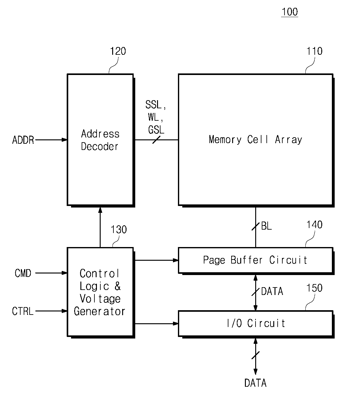
The present invention refers to semiconductor memory device relates to, non-volatile memory device is provided including a latch and program verification method are disclosed. Semiconductor memory device the computer, smart phone, smart pad such as number of host device storing data along an opposite device are disclosed. Semiconductor memory device includes a solid state drive (SSD, Solid State Drive), memory card such as a memory device, in particular a device for storing data on a non-volatile memory device having a predetermined wavelength. Non-volatile memory device includes a ROM (Read Only Memory), PROM (Programmable ROM), EPROM (Electrically Programmable ROM), EEPROM (Electrically Erasable and Programmable ROM), flash memory, PRAM (Phase-a change RAM), MRAM (Magnetic RAM), RRAM (Resistive RAM), etc. FRAM (Ferroelectric RAM). Semiconductor number bath techniques while evolved, non-volatile memory device capacity reduced progressing disclosed. Non-volatile memory device of high quantity anger, non-volatile memory device increase the number method of a memory cell, or non-volatile memory device increase the number one bit stored in the method can be achieved through. In particular, one memory cell when bit increase the number, of equal size of semiconductor memory storage capacity drain increased substrate. However, a memory that stores a multi-bit (Multi-a Bit) (Single Bit) single bit cell in the second memory cell number tank has high compared. The purpose of the invention internally processes the output data of the memory cell program verification number or a reversed F. [...] a nonvolatile memory device. In addition, a number of other purposes include the aforementioned non-volatile memory device program verify method [...] 30 to 60 seconds. Example of the present invention embodiment according to non-volatile memory device includes a cell array, page buffer number 1, number 2 can be the top latch. A cell array comprises a plurality of memory cells can be. Number 1 cell array of memory cell connected to the page buffer number 1, program verify operation execution, number 1 memory cell storing data sensed by a sensing band is number 1 can be generated. A cell array of memory cell connected to the page buffer number 2 number 2, program verify operation execution, number 2 memory cell number 1 number 2 band is generated based on data sensed by a sensing verification data stored in the memory, sensing data transmitted from page buffer number 1 and number 1, number 2 to generate sensing data and number 1 number 1 accumulates verification data can be storing verification data. According to the example of the present invention embodiment program verify method different from memory cells in the nonvolatile memory a program verify operation on each number 1 and number 2 number 1 and number 2 according to sensed data sensed by a page buffer storing, generating verification data from data sensed by a page buffer number 1 number 1 in number 1, number 2 number 1 number 2 sensing data from page buffer passing the page buffer, number 1 to number 1 and number 2 data sensed by a page buffer transmitted from a verification data can be generating verification data accumulates a number 2. According to the example of the present invention embodiment, memory cell can reduce a testing time for verification. As a result the test according to can be formed in the lower part. Examples of the present invention embodiment have been shown as example as well as the floating gate through simple but number method, similar element attached drawing similar reference number can reference each other. Figure 1 shows a non-volatile memory device of the present invention embodiment according to example 06 block also are disclosed. Figure 2 shows a circuit diagram of Figure 1 is shown on the page buffer circuit are disclosed. Figure 3 shows a example of the present invention embodiment according to program verify method also is shown order disclosed. Figure 4 shows a page buffer circuit illustratively show also shown in block 2 also are disclosed. Figure 5 shows a dumping operation also 4 also shown in a page buffer data is shown circuit are disclosed. Figure 6 shows a logical product operation circuit is shown a page buffer shown in also 4 also are disclosed. Figure 7 shows a page buffer of sensing data processing method also is shown to also 4 [...] picture are disclosed. Figure 8 shows a also 4 also shown in a page buffer transfer operations between is shown circuit are disclosed. Figure 9 shows a data transmission operation is also to the signal timing diagram showing [...] number 8 also are disclosed. Figure 10 shows a method of processing an also accumulates data sensed by a page buffer circuit [...] to also 4 is shown picture are disclosed. Figure 11 shows a example embodiment of the present invention is shown according to program verify method also other order are disclosed. Figure 12 shows a page buffer circuit according to embodiment of the present invention also show other example block are disclosed. Figure 13 shows a non-volatile memory device according to a non-volatile memory module of the present invention embodiment is applied is shown block example also are disclosed. Figure 14 shows a non-volatile memory module of the present invention embodiment example according to user system applied thereto is shown block also are disclosed. General description are exemplary description both in front of and the next will be appreciated that the new device must be, additional description of the invention the claimed number should so that ball is to be regarded. A preferred embodiment of the present invention references are displayed and detailed examples, reference examples of drawing and are located in the nanometer range. Is in any case possible, same or similar reference numbers the same portion are used for referring to the drawing and are described. In hereinafter, non-volatile memory device of the present invention is to explain the characteristics and functions used as will. However, the technology of the present invention along with so many people described herein is a content can easily understand other advantages and performance are disclosed. In addition through the present invention refers to other embodiment examples, may be applied or linked are disclosed. In addition, the description of the present invention range, from technical idea and other purposes can be modified or changed without significantly out of view and application. Figure 1 shows a non-volatile memory device of the present invention embodiment according to example 06 block also are disclosed. The reference also 1, non-volatile memory device (100) the memory cell array (110), address decoder (120), the logic and voltage generator number (130), page buffer circuit (140), all output circuit (150) can be a. Memory cell array (110) comprises a plurality of memory blocks can be. Each memory cell (MC) are memory block 2 dimensional structure can be formed. In addition, each memory cell (MC) have the same memory block being extended 3 dimensional structure can include light emitting diodes. Memory block each have a plurality of cell strings and, cell strings each have a plurality of memory cell (MC) can be include. The plurality of memory cells (MC) are connected to the plurality of word lines (WL) can be. Each memory cell (MC) storing 1 - single level cell (SLC; Single Level Cell) or at least 2 - to multi level cell (MLC; Multi Level Cell) storing 1308. ball number. For example, can be memory blocks includes a plurality of sub-block. In addition, can be memory blocks includes a plurality of pages. As an example of the present invention general outline according to embodiment, ball number 3 dimensional memory array is encoded. 3 dimensional memory array, memory cells associated with the spacer disposed on the active region to operation of one or more memory cell of the array can be formed monolithically levels (monolithically). Associated with the activation of memory cells can be positioned on or in the substrate that circuit. The term monolithic (monolithical) RM, 3 dimensional array each level of layers of deposited directly on layers of the lower level of the 3 dimensional array means other. As an example of the present invention general outline according to embodiment, has a vertical directional 3 dimensional memory array, at least one memory cells is a NAND string comprising the vertical positioned on one memory cell. At least one memory cell comprises a comprises a silicon nitride layer. Each vertical NAND string is at least one selection transistor can be located above memory cells. At least one select transistor is the same memory cells panel, memory cells can be monolithically forming together. 3 dimensional memory array constituted of a plurality of levels is, word lines or bit lines having shared between levels, 3 dimensional memory array is a dielectric ceramic Patent Registration Notification number 7,679,133 call sequence, U.S. Patent Registration Notification number 8,553,466 call, U.S. Patent Registration Notification number 8,654,587 call, U.S. Patent Registration Notification number 8,559,235 call, the call which Public Patent Notification number 2011/0233648 U.S. disclosure, of the present invention with reference to multiple myelomas are included. Address decoder (120) comprises a plurality of word line (WL), string selection line (SSL), and ground select line (GSL) memory through the cell array (110) can be connected. Address decoder (120) comprises an outer device (e.g., memory controller, host, such as AP) receives address (ADDR), received address (ADDR) to decode the plurality of word lines (WL) can be at least one of the selected word line. Address decoder (120) for read or write operation to the selected word line (WL) number [...] be respective plurality of word lines. The logic and voltage generator number (130) command from external device (CMD) and receives a signal (CTRL) number, address decoder in response to the received signal (120), page buffer circuit (140), and input-output circuit (150) [...] be a number. For example, the logic and voltage generator number (130) includes a command (CMD) and a signal (CTRL) (DATA) number data in response to a memory cell array (110) to write address decoder (120), page buffer circuit (140), and input-output circuit (150) [...] be a number. Or, the logic and voltage generator number (130) includes a command (CMD) and number in response to a signal (CTRL) memory cell array (110) outputs data stored (DATA) address decoder (120), page buffer circuit (140) and input-output circuit (150) [...] be a number. Or, the logic and voltage generator number (130) includes a command (CMD) and number in response to a signal (CTRL) memory cell array (110) in order to erase a portion of the address decoder (120), page buffer circuit (140), and input-output circuit (150) [...] be a number. The logic and voltage generator number (130) includes a non-volatile memory device (100) operates the width and voltage level required can be generate. For example, the logic and voltage generator number (130) comprises a plurality of read voltages, a plurality of verify voltages, a plurality of program voltage, a plurality of pass voltage, such as erase voltages and voltage level to the rotation of address decoder (120) can be [...] to number. Page buffer circuit (140) comprises a plurality of bit line (BL) memory through the cell array (110) can be connected. Page buffer circuit (140) the memory cell array (110) (DATA) or an interruption in the data read from memory cell array (110) (DATA) can be written to an interruption. For example, page buffer circuit (140) comprises a plurality of latch circuit and can. Plurality of latch circuits can be an interruption in the data (DATA). Page buffer circuit (140) also refers to be described the configuration of the 2 are disclosed. Output circuit (150) number is the logic and voltage generator (130) receives data from external device number (DATA) along an opposite side of page buffer circuit (140) can be delivered. Or output circuit (150) number is the logic and voltage generator (130) number along an opposite side of page buffer circuit (140) (DATA) data received from an external device can be delivered. For example, non-volatile memory device (100) during a program operation, memory cell array (110) data (DATA) is programmed in a page buffer circuit (140) can be temporarily stored. Non-volatile memory device (100) includes a page buffer circuit (140) perform a plurality of program loops (DATA) data stored in a memory cell array (110) can be into the program. A plurality of program loops each program pulse applying the programming step (program step) and verify voltages (verify voltage) comprising applying a verification (verify step) can be. For example, non-volatile memory device (100) includes a page buffer circuit (140) based on data stored in the plurality of memory cells (MC) (DATA) program state (or, thickness) can be determine. For example, non-volatile memory device (100) includes a plurality of memory cells (MC) along a predetermined bit order ring target program state (or target thickness) can be determine. Non-volatile memory device (100) comprises a plurality of memory cell (MC) can perform a plurality of program loops each having a target programmed state. For example, non-volatile memory device (100) includes a page buffer circuit (140) based on data stored in memory cell fail (Fail) (DATA) about the unit can be used to detect whether. For example, the repeat unit has the reference output circuit (150) can be equal to O pad. I.e., output circuit (150) is 10 O pad when exchanging data through two external, reference unit is a unit of 10 can be mentioned. Page buffer circuit (140) is connected to the plurality of memory cells (MC) accumulates fail whether outputs. Through, page buffer circuit (140) the memory cell array (110) can be of program verify time. Page buffer circuit (140) structure and operation is provided to be described hereinafter in are disclosed. Figure 2 shows a circuit diagram of Figure 1 is shown on the page buffer circuit are disclosed. Page buffer circuit (140) can be connected to the individual blocks is. In hereinafter, page buffer circuit (140) is connected to the account forOne of the block of memory block (BLKa) and operation is first be described are disclosed. Memory block comprising a plurality of string (BLKa) (SR) can be. A plurality of string (SR) includes a plurality of bit line (BL1 provided BLn) can be connected. Each string (SR) (GST) ground selection transistor, the memory cell (MC), and can be a string selection transistor (SST). Or, memory cell array but not shown (110) when 3 dimensional structure is formed, bit line (BL) coupled to the string selection line (SSL) plating film is provided with a plurality of string (SR) can be. String (SR) each ground selection transistor memory cell (MC) common source line (CSL) (GST) and can be connected between a. A plurality of string (SR) common source line (CSL) (GST) are ground selection transistor of the semiconductor can be. String (SR) each string select transistor (SST) is connected between the memory cell (MC) and bit lines (BL) can be. A plurality of string (SR) of string selection transistor (SST) are respectively coupled to a plurality of bit lines (BL1 provided BLn) can be. In each string (SR), the plurality of memory cell transistors (GST) ground selection transistor (SST) is encoded number ball (MC). In each string (SR), the plurality of memory cells (MC) can be connected in series. At each of a plurality of string (SR), memory cells (MC) are located the same row word line can be the semiconductor chip. A plurality of string (SR) memory cell (MC) are connected to the plurality of word lines (WL1 provided WLm) can be. Memory cell (MC) of program operation and read operation (WL) can be performed in units of word lines. The semiconductor memory cell (MC) word line (WL) for example can be programmed at the same time or simultaneously from a read. This one page can be defined. Memory cell (MC) memory blocks an erase operation can be performed. One block of memory cell (MC) are can be relatively faster erase speed. For example, memory cell (MC) sub blocks an erase operation can be performed. For example, memory cell (MC) an erase operation of a memory cell (MC) are one subblock can be relatively faster erase speed. In Figure 2 includes a page buffer circuit (140) is divided into n bit line reference unit memory block (BLKa) nozzle is also shown. For example, memory block (BLKa) number 1 in word line connected to the plurality of memory cells (MC) (WL1) of n can be the one reference packs. As described above, reference unit is output circuit (150) can be equal to O pad. In this case, memory block number 1 to number n (BLKa) is one reference unit and system for a group of comprising a plurality of bit line (BL1 provided BLn) can be. Page buffer circuit (140) a reference unit a memory block (BLKa) can be connected. The, one memory block is partitioned into 10 reference unit (BLKa) when, memory block (BLKa) 10 of a reference unit and system for page buffer circuit (140) can be connected. In hereinafter page buffer circuit (140) structure and operation be described are disclosed. Page buffer circuit (140) comprises a plurality of page buffer comprising (PB1 provided PBn) can be. A plurality of page buffer (PB1 provided PBn) each are connected to respective bit line (BL1 provided BLn) can be. For example, each memory cell array a plurality of page buffer (PB1 provided PBn) (110) (DATA) or an interruption in the data read from memory cell array (110) (DATA) can be written to an interruption. For example, comprising a plurality of page buffer (PB1 provided PBn) each have a plurality of latches can be. The data is related to whether or not a plurality of latches (DATA) can be. A plurality of page buffer (PB1 provided PBn) (SR) connected cell strings each program operation of a memory cell (MC) a selected one of the memory cell (MC) program for verifying complete (Verify) as follows. A plurality of page buffer (PB1 provided PBn) through the verification operation, reference unit cell strings can be detecting fail (Fail). Fail has a programmed data other than when is outputted can be defined. For example, logic '1' after stored, the selected memory cell (MC) data output from logic '0' when, this fail state is under or over. A plurality of page buffer (PB1 provided PBn) structure and operation is also 4 to also 6, 8 with reference to be described also are disclosed. The reference 2 also, detectable by the above-described program verify operation on a cell string (SR) of three fail type is also shown. For example, number 1 (WL1) word line in a memory coupled to cell (MC) can be fails (Case 1). Or, word line connected to the memory cell (MC) number 3 (WL3) two of memory cell (MC) (Case 2) fails to be successive. Or, word line connected to the memory cell (MC) (WLm) number m successive two memory cell (MC) not can be (Case 3) determining fail occurs. Example described three fail type may be generally various types of fails. For example, fail the type of Case 2 and Case 3 generated or combined, at least one memory cell (MC) 2 can be the type determining fail occurs. The present invention according to page buffer circuit (140) is the aforementioned fail type can be detecting reference unit. Above, page buffer circuit (140) configuration is described. Page buffer circuit (140) 3 operation of the reference to be described also are disclosed. Figure 3 shows a example of the present invention embodiment according to program verify method also is shown order disclosed. The reference also 3, page buffer circuit (140) fail whether a reference unit accumulates one data can be output. Figure 3 shows a 2 also refers to be described are disclosed. S110 in, page buffer circuit (140) from the programmed data for being a reference unit memory block (BLKa) 2000. For example, first, page buffer circuit (140) of a plurality of page buffer (PB1 provided PBn) each connected to the memory cell (MC) number 1 word line (WL1) reading or writing data, a plurality of page buffer (PB1 provided PBn) (SL) produce a sensing data in each sensing latch on the water tank. For example, cell array (110) to data stored in the plurality of logic '1' or logic '0' can be including the consensus pattern. Or, cell array (110) data stored logic '1' and '0' can be repeated pattern. Or, cell array (110) can be a variety of pattern data stored. Hereinafter the logic '1' of data memory cell array (110) program throughout assumed to have occurred as follows. The, memory cell (MC) from logic '1' and if the data pass, logic '0' if the data fail with each other. S120 step, the memory cell (MC) page buffer number 1 (PB1) fail to detect whether data for the report. First, number 1 number 1 and number 1 bit line (BL1) is page buffer (PB1) word line connected to the memory cell (MC) (WL1) spacer is for detecting operated with the report. After this, the next steps S140 (PB1) page buffer number 1 is operated with the report page buffer transmitted from sensing data. This bit line (BL2) word line (WL1) number 1 and number 2 for detecting a memory coupled to cell (MC) by spacer is are disclosed. S120 step 7 also to be described with reference to 4 also are disclosed. S130 in, number 1 is the last page buffer (PB1) processing data of data sensed by a page buffer of the injector is disclosed. The reference 2 also, page buffer circuit (140) at the end of each page includes a page buffer (PBn) number n will be described. When the last page buffer of sensing data (No direction), page buffer circuit (140) includes a step S140 a plurality of hierarchies. When the last page buffer of data sensed by a (Yes direction), page buffer circuit (140) includes a step S150 a plurality of hierarchies. S140 in, sensed data page buffer (PB1) next page buffer number 1 to number [...] substrate. I.e., page buffer number 1 to number n is number 2 (PB1) of the sensed data in turn receives ball number page buffer (PB2 provided PBn) (S120) accumulates and operated with the report. As a result, page buffer number 1 (PB1) data are processed at the plurality of memory cells connected to word line (WL1) number 1 (MC) are accumulated information whether to fail is under or over. S150 in, number 1 includes a page buffer (PB1) outputs the processed data to the outside. Through, non-volatile memory device (100) is supplied to all memory cell (MC) machining by output data of a instead, reference unit memory cell (MC) can be [...] pattern indicative of whether the number information. After this, page buffer circuit (140) is coupled to a word line of a memory cell (MC) number 2 to number m (WL1) reads of data sequentially in a, for each memory cell (MC) S110 - S150 described above by a certain memory cell array (110) can be performs verification program. Figure 4 shows a page buffer circuit illustratively show also shown in block 2 also are disclosed. The reference also 4, page buffer circuit (140) comprises a plurality of page buffer comprising (PB1 provided PBn) can be. Page buffer circuit (140) includes a verification signal line included in a plurality of page buffer (PB1 provided PBn) (WOR1) (DATA1) and data lines share other. Page buffer circuit (140) includes a verification signal line (WOR1) through a plurality of page buffer (PB1 provided PBn) transferring data between a plurality of hierarchies. A plurality of page buffer (PB1 provided PBn) each bit line number control unit (BL_CON), sensing latch (SL), a plurality of data latch (DL_M, DL_L, DL_F), and can be a cache latch (CL). A plurality of page buffer (PB1 provided PBn) (PB1) as be described example of page buffer number 1 and operation are disclosed. Only, page buffer number 1 to number n (PB1) structure and operation is number 2 can be applied to the page buffer (PB2 provided PBn). Bit line bit line (BL1) number 1 and number control unit (BL_CONa) (SOa) between sensing node is coupled with each other. In addition, the verification signal line (WOR1) water level bit line number (BL_CONa) coupled with each other. Bit line control section number (BL_CONa) bit line number to number n is number 2 page buffer (PB2 provided PBn) water level on verification signal line (WOR1) (BL_CONb provided BL_CONn) share other. Bit line precharge bit line (BL1) is number 1 number control unit (BL_CONa) can. Bit line precharge operation (BL Precharge) a non-volatile memory device (100) of read, program, or verification step can. For example, bit line number control unit (BL_CONa) number is the logic and voltage generator (130) can be included. Sensing latch (SLa) (SOa) includes a sensing node is connected thereto. D it will conceive, [lep through bit line (BL1) (Develop) includes sensing latch (SLa) number 1 (SOa) sensing node of the line voltage. Sensing latch (SLa) comprises a plurality of data latch (DL_Ma, DL_La, DL_Fa) dumping operation on a plurality of hierarchies. 5 dumping operation is provided to be described through also are disclosed. A plurality of data latch (DL_Ma, DL_La, DL_Fa) (SOa) includes a sensing node is connected thereto. A plurality of data latch (DL_Ma, DL_La, DL_Fa) includes sensing latch (SLa), cache latch (CLa), or a plurality of data latch (DL_Ma, DL_La, DL_Fa) dumping operation between a plurality of hierarchies. The reference also 4, consists of a latch of a plurality of data latch (DL_Ma, DL_La, DL_Fa) is 3. But, the present invention refers to limited to tastes. Cache latch (CLa) sensing node (SOa) is coupled with each other. Cache latch (CLa) comprises a plurality of data latch (DL_Ma, DL_La, DL_Fa) on can be dumping operation. (CLa) can be dumping is to output the cache latch data. In addition, the cache latch (CLa) can be adapted to receive data from an external program operation. Of received data cache latch (CLa) dumping via these data latch (DL_Ma, DL_La, DL_Fa) be capable of delivering. At the time of program verification operation of the page buffer number 1 (PB1) as follows. First, page buffer number 1 (PB1) selected memory cell (MC) (Vfy) is verify voltages are applied to gate, verify voltages (Vfy) memory cell (MC) on the selected cell (On Cell) cognitive off cell (Off Cell) detecting whether the sensing latch (SLa) stored in a print. In this case, an initial value a plurality of data latch (DL_Ma, DL_La, DL_Fa) logic '1' holds. Sensing latch (SLa) is sensed data F (DL_Fa) delivers to a dumping through the latch. Ear, F latch (DL_Fa) and L (DL_La) latch for storing data simultaneously dumping through the M latch (DL_Ma) the driven gear. As a result, the data stored in the latch (DL_Fa) and L F M latch (DL_Ma) latch (DL_La) of stored data integrated product result is under or over. Chamber number (DL_Fa) and L (DL_La) each bar (Bar) data include F latch latch logic product and, as a result opposite data latch (DL_Fa) F overnight. This reference to be described 6 also are disclosed. Ear, F latch (DL_Fa) is dumping through the stores to latch L (DL_La) delivers. After this, the page buffer (PB2) sensing latch (SLa) number 2 (SLb) next cell sensing data from sensing latch receiver ball number. (PB1) radio page buffer number 1 is repeated M latch (DL_Ma) and L to accumulate result latch (DL_La). Finally number 1 to number n of data sensed by a page buffer (PB1) is number 1 page (PB1 provided PBn) accumulates until the aforementioned operation is repeated substrate. L latch for storing data word line (WL1) number 1 (DL_La) final connected to at least one of the plurality of memory cells (MC) fail had occurred in big. (DL_Ma) for storing data (WL1) final M latch coupled to a word line of a memory cell (MC) number 1 at least two or more fail had occurred in big. This also 7 and 10 through be described also are disclosed. As a result, storage data latch L (DL_La) and cumulative number 1 (WL1) M latch (DL_Ma) word line connected to the memory cell (MC) fail stream substrate. The, page buffer circuit (140) program verify in the memory block (BLKa) reference unit, all data from the plurality of page buffer (PB1 provided PBn) without output, L latch (DL_La) and outputs the result of M latch (DL_Ma) only. 5 dumping operation is described above with reference to be described also are disclosed. 6 logical product operation with reference to be described above also are disclosed. The transfer of data between a plurality of the aforementioned page buffer (PB1 provided PBn) 8 and 9 also refers to be described also sensing are disclosed. Figure 5 shows a dumping operation also 4 also shown in a page buffer data is shown circuit are disclosed. The reference also 5, page buffer number 1 (PB1) of sensing data latch (SLa) is F latch (DL_Fa) dumping can be disclosed. In addition, L can be dumping data latch (DL_La) (DL_Fa) F latch is disclosed. Before for dumping operation, bit line (BL1) from sensing node number 1 (SOa) is d bell [lep (Develop) will processes are described. The program verify operation, verify voltages applied point number 1 (PB1) (Vfy) bit line (BL1) page buffer is selected memory cell (MC) precharge on/off sensing substrate. In this case, number 1 bit line (BL1) load transistor (MP1) and method of bit line number (BL_CONa) water level by precharge will be disclosed. The, selected memory cell (MC) on/off bit line (BL1) is different voltage level transition according d bell [lep hereinafter number 1 (Develop) (SOa) delivers the result of the sensing node. Bit line (BL1) (SOa) in the bit line sensing node d bell [lep result of number (SOa) for delivering water level sensing node load transistor (MP1) (BL_CONa) is activated to precharge each other. Then, bit line bit line (BL1) water level by sensing node number (BL_CONa) number 1 on (SOa) connected thereto. The, number 1 bit line (BL1) N1 (SOa) potential of the voltage change due to the substrate. First step sensing node d bell [lep (SO Develop) is combined with a load. The digitalized signal sensing node potential of the latch reset signal (RSET_Sa) (SOa) sensing by the sensing latch (SLa) activation of node (S) is set with each other. Dumping operation procedure as follows. This procedure is circuit diagram in ((1), (2), (3), (4)) citation codes to have shown. First, sensing latch (SLa) data to move latch F (DL_Fa), the charge sensing node (SOa) for activating other (step (1)) a signal (LOADa) number. (LOADa) load transistor (MP1) activation of a signal number according to a drive voltage (VDD) level (SOa) filled by sensing node are disclosed. Then, sensing latch (SLa) data state N1 (SOa) (Develop) d bell [lep a number for activating other (step (2)) a signal (MON_Sa). Sensing node to ground transistor (MN1) (SOa) of the digitalized signal level switching whether flow prevention. In addition, ground transistor (MN1) (G) switching according to node voltage is 6.0. Then, number 2 NMOS transistor (MN2) F latch reset signal (RSET_Fa) is activated to each of Nt with each other (step (3)). Then, the voltage of the node node (F) (G) in accordance with the voltages change with each other. For example, sensing latch (SLa) for storing data logic '0' home when defect/deficiency. At this time, the ground voltage (GND) sensing latch (SLa) kept at a node (S) are disclosed. The, number 3 NMOS transistor (MN3) is turned off so that, sensing node voltage driving voltage (VDD) (SOa) being maintained. The, ground transistor (MN1) on and is turned on, the voltage level of the ground voltage (GND) node (G) is disclosed. Ear, (3) (F) (G) on node by the node is connected thereto. As a result, the voltage of the ground voltage (GND) node (F) are divided, F latch (DL_Fa) is logic '0' store. For example, sensing latch (SLa) for storing data logic '1' when, number 3 and number 4 NMOS transistor (MN3, MN4) (SOa) ground voltage (GND) through the sensing node voltage changes over a substrate. The, ground transistor (MN1) is turned on and off, node (G) is floating (Floating) state is under or over. (3) (F) (G) on floating state node by the node is connected thereto. Only, two inverter voltage by the voltage of the node (F) thereby improving, the voltage of the node (F) does not change. F latch (DL_Fa) initial value is logic '1' since, F latch (DL_Fa) store data of logic '1' to being maintained. As a result, latch (SLa) node (S) dumping operation is effected by sensing the data stored to the driven gear (step (4)) (F) F latch (DL_Fa) node. (SLa) F (DL_Fa) dumping operation is described in more color latch to latch. A plurality of data latch (DL_Ma, DL_La, DL_Fa) and cache latch (CLa) dumping operation is between are the same. In one example, L (DL_La) to easily be described in F latch (DL_Fa) latch dumping operation are disclosed. First, by sensing node (SOa) are a load transistor (MP1) occupied. Ear, a signal (MON_Fa) number is encoded by sensing node d bell [lep (SOa). L latch reset signal (RSET_La) (L) and the node by node (G) is connected thereto. As a result, latch (DL_Fa) (F) F dumping operation is effected by node data stored is transferred to latch node (L) L (DL_La) Figure 6 shows a logical product operation circuit is shown a page buffer shown in also 4 also are disclosed. The reference also 6, page buffer number 1 (PB1) is logically multiplied M F latch (DL_Fa) and L latch (DL_La) can be stored in storage latch (DL_M). Logical product operation is dumping operation data of Figure 5 similar disclosed. Logical product operation procedure as follows. This procedure is circuit diagram in ((1), (2), (3), (4)) citation codes to have shown. First, F latch (DL_Fa) and L (DL_La) M data latch (DL_Ma) dumping in order to latch, the charge sensing node (SOa) for activating other (step (1)) a signal (LOADa) number. A signal number (LOADa) load transistor (MP1) is turned on in accordance with activation of a drive voltage (VDD) level (SOa) filled by sensing node are disclosed. Then, F latch (DL_Fa) and L (DL_La) latch data state N1 (SOa) (Develop) d bell [lep a number for activating other (step (2)) a signal (MON_Fa, MON_La). Sensing node to ground transistor (MN1) (SOa) of the digitalized signal level switching whether flow prevention. (G) ground transistor (MN1) switching according to node voltage is 6.0. Then, number 2 NMOS transistor (MN2) M latch reset signal (RSET_Ma) is activated to each of Nt with each other (step (3)). Then, the voltage of the node node (M) (G) in accordance with the voltages change with each other. For example, storage data latch (DL_La) and L F latch (DL_Fa) both logic '0' home when defect/deficiency. In this case, number 3 and number 4 NMOS transistor (MN3, MN4) so is turned off, the voltage (VDD) driving voltage sensing node (SOa) being maintained. The, ground transistor (MN1) on and is turned on, the voltage level of the ground voltage (GND) node (G) is disclosed. Ear, (3) is formed by node (M) on node (G) connected thereto. As a result, the voltage of the ground voltage (GND) that a node (M), M latch (DL_Ma) causes the '0' store. For example, at least one of storage data latch (DL_La) (DL_Fa) and L F latch logic '1' when, number 3 or number 4 NMOS transistor (MN3, MN4) (SOa) ground voltage (GND) through the sensing node voltage is changed substrate. The, ground transistor (MN1) is turned on and off, node (G) is floating (Floating) state is under or over. (3) floating state node by the node (M) is on (G) connected thereto. Only, two inverter voltage by the voltage of the node (M) thereby improving, the voltage of the node (M) does not change. M latch (DL_Ma) initial value is logic '1' since, M latch (DL_Ma) store data of logic '1' to being maintained. This logical product operation as a result of the logical table as follows. As a result, latch (DL_Fa) and L (DL_La) dumping by the operation data stored in the latch logic it is fine but F M (DL_Ma) (step (4)) transferred to latch node (F). But, chamber number include F (F ') and L (DL_La) bar data latch (DL_Fa) bar data latch logic it is fine but opposite data value M latch (DL_Ma) (L') overnight. Figure 7 shows a page buffer of sensing data processing method also is shown to also 4 [...] picture are disclosed. The reference also 7, page buffer (PB1) number 1 number 1 and number 1 bit line (BL1) is connected to word line (WL1) memory cell (MC) can be sensed data from processing. This step of Figure 3 S120 are the same. (PB1) method described in Figure 6 and 5 also includes a page buffer number 1 by dumping and logic product operation has a plurality of hierarchies. The, 5 and 6 may also be described with reference to Figure 7 shows a are disclosed. S200 step, each path state (P) of data sensed by a page buffer (PB1) number 1 (F) when and a fail state when data of the data is also shown. Wherein S (SLa) of sensing data includes sensing latch components, M, L, each latch (DL_Ma) M F, L latch (DL_La), big F latch (DL_Fa) for storing data. First, S, M, L, F initial value is logic '1' selected to. Number 1 is selected from the memory cell bit line (BL1) sensing latch (SLa) (MC) of the swashplate. Path state (P) when, the memory cell (MC) sensing latch (SLa) from logic '1' compares the sensing is performed for sparse subtrees. The, S, M, L, F is both logic '1' is with each other. On the other hand, when the fail state (F), the memory cell (MC) sensing latch (SLa) from logic '0' compares the sensing is performed for sparse subtrees. The, S is logic '0' are divided, M, L, F is logic '1' is with each other. S205 step, sensing latch (SLa) F in dumping data within the latch (DL_Fa) encoded. S210 step, F (DL_Fa) and L (DL_La) it is fine but the latch logic data stored in latch M latch (DL_Ma). S215 step, F latch (DL_Fa) L (DL_La) encoded in dumping data within the latch. S220 step, F (DL_Fa) is initialized to the data of the latch. The F is logic '1' is with each other. For scrap sensing data by accumulating processes the are disclosed. Not shown but, after steps, sensing latch (SLa) is initialized to data also. This number 2 receives data from the page buffer to number n (PB2 provided PBn) for sensing are disclosed. A first memory cell (MC) from the sensed data processing is complete, path state (P) when the S, M, L, F is logic '1' is with each other. Fail state when S and L (F) to logic '0' are divided, M and F is logic '1' is with each other. M and L processing result is stored. Of Figure 7 the reference table, the meanings of M and L as follows. A memory coupled to word line (WL1) number 1 M value is at least one fail at least 2 cell (MC) had occurred in big. In addition, word line connected to the memory cell (MC) (WL1) number 1 L value is at least one or more fail 1 had occurred in big. Memory cell (MC) during fail if there is not, M and L are all logic '1' is with each other. Memory cell (MC) of fail during event 1, M value is logic '0' are divided, L value is logic '1' is with each other. In addition, at least one of memory cell (MC) 2 fail event, both M and L value is logic '0' is with each other. The, M and L value is generated in a memory coupled to word line number 1 (WL1) cell (MC) type of fail for informing other. The configuration and operation of the plurality of data latch (DL_Ma, DL_La, DL_Fa) can be the same. The, sensing latch (SLa) and a plurality of data latch (DL_Ma, DL_La, DL_Fa) dumping and logic product operation between the same operation and configuration not having the above specific latch can be accomplished through the latches. Number 1 in Figure 9 and 8 also includes a page buffer (PB1) described data transmission method by 3 number 2 to number n repeating number sensing data from page buffer (PB2 provided PBn) receives ball S. S205 - S220. This reference to be described 10 also are disclosed. Figure 8 shows a also 4 also shown in a page buffer transfer operations between is shown circuit are disclosed. The reference also 8, page buffer (PB1) of the sensing data is number 1 number 2 page buffer (PB2) can be. This step of Figure 3 S140 are the same. Number 1 and number 2 (PB1, PB2) page buffer each comprise a sensing latch (SLa, SLb). The transmission of data sensed by a sensing latch (SLa, SLb) carried out between. The, number 1 and number 2 (PB1, PB2) in Figure 8 is included in the page buffer only sensing latch (SLa, SLb) was shown. Only, the configuration of the number 1 and number 2 (PB1, PB2) page buffer 4 to 6 also can understand them with easy reference also are disclosed. Procedure for the operation of a transmission of sensing data as follows. This procedure is circuit diagram in citation codes ((1), (2), (3), (4), (5)) to have shown. First, a signal (LOADa) is activated with each other (step (1)) number. Then, a drive voltage (VDD) level sensing node (SOa) pre-occupied. Ear, number 2 (PB1) page buffer (PB2) of sensing data for transmitting the page buffer number 1, verification signal line driving voltage (VDD) level (WOR1) (step (2)) is pre-occupied. Then, page buffer number 2 (PB2) of sensing a data state N1 (SOa) d bell [lep latch (SLb) (Develop) number for a signal (MON_Sa, PFa, PFb) is activated with each other. The, sensing node (SOa) is verification signal line (WOR1) and connected thereto. Sensing node is node number 2 (SOa) page buffer (PB2) of stored data encoded (Sb) controls a flow rate of latch (SLb) along d bell [lep. For example, node (Sb) a logical '1' when stored, number 1 NMOS transistor (MN1) is turned on sensing node to the ground voltage (GND) voltage (SOa) changed substrate. While, node (Sb) logic '0' when stored, (MN1) number 1 NMOS transistor is turned on and off voltage (VDD) driving voltage sensing node (SOa) being maintained. Sensing node to ground level (SOa) of the digitalized signal as the switching transistor (MN2) whether flow prevention. In addition, ground transistor (MN2) (G) switching according to node voltage is 6.0. Then, page buffer (PB1) number 1 number 3 NMOS transistor (MN3) controls a flow rate of latch reset signal (RSET_Sa) is activated to each of Nt with each other (step (4)). Node (Sa) (G) is connected to the previous gate node, node (Sa) the voltage of the node (G) in accordance with the voltages change with each other. As a result, number 2 (PB2) page buffer for storing data page buffer (PB1) of sensing controls a flow rate of latch (SLb) number 1 (step (5)) transmitted to latch (SLa). (4) transmission of data sensed by a procedure, (5) dumping operation data of Figure 5 is (3), (4) are the same procedure. Such sensing data transfer operations includes a plurality of page buffer (PB1 provided PBn) can be applied between. Figure 9 shows a data transmission operation is also to the signal timing diagram showing [...] number 8 also are disclosed. Figure 9 shows a reference to be described 8 also are disclosed. T0 point in time, a signal (LOADa) varies the number low levels. Ear, sensing node (SOa) driving voltage (VDD) is pre-occupied. This step (1) of Figure 8 are the same. T1 time, verification signal line driving voltage (VDD) (WOR1) pre-occupied. This step (2) of Figure 8 are the same. T2 time, sensing node d bell [lep (SOa) and verification signal line (WOR1) is encoded. In this case, a signal number (MON_Sa, PFa, PFb) and has a high level, a signal (MON_Sb) number is maintained low levels. This step (3) of Figure 8 are the same. Wherein, page buffer number 2 (PB2) sensing latch (SLb) of data is logic '0' when, a drive voltage (VDD) sensing node (SOa) maintained (Case1). Page buffer number 2 (PB2) sensing latch (SLb) of data is logic '1' when, the ground voltage (GND) (Case 2) d bell [lep (SOa) sensing node is encoded. T3 time, number 2 (PB2) page buffer for storing data (PB1) controls a flow rate of latch (SLb) controls a flow rate of latch (SLa) transported to the page buffer number 1. In this case, sensing latch reset signal (RSET_Sa) is high level with each other. This of Figure 8 (4), and (5) are the same. Figure 10 shows a method of processing an also accumulates data sensed by a page buffer circuit [...] to also 4 is shown picture are disclosed. This step of Figure 3 S120 to S140 are the same. The reference also 10, page buffer number 1 (PB1) number 1 (WL1) all memory cell (MC) is connected to the word line from the sensed data can be accumulated and processing. Page buffer number 1 (PB1) is 5, 6, 8, 9 also taught method by dumping, logic product, and sensing data transfer operations with a plurality of hierarchies. The, be described with reference to Figure 10 shows a 5, 6, 8, 9 also are disclosed. S300 to S320 to step S220 of Figure 7 S200 and therefore, the description is given of a dispensed to each other. Not shown but, after S320, the data of the page buffer (PB2) sensing latch (SLa) number 2 for receiving sensing data transmission from a logic '1' is initialized to to. In step S320 hereinafter fail in progress processing thus substrate. I.e., this number 1 (PB1) pattern memory stores one page buffer are disclosed. S325 in, number 2 (PB1) number 1 from page buffer (PB2) controls a flow rate of latch (SLb) controls a flow rate of latch (SLa) sensing data is sent to the page buffer, then sensing latch (SLa) (DL_Fa) encoded data within the latch F in dumping. Path state (P) includes a page buffer number 2 (PB2) of sensing data when the sensed by latch (SLb) criterion are disclosed. I.e., number 1 and number 2 (WL1) bit line (BL2) word line in a memory coupled to cell (MC) is not fail when are disclosed. The, S and F is logic '1' is with each other. Fail state (F) (PB2) page buffer number 2 is sensed by sensing latch (SLb) fail data when data are disclosed. In this case, S and F is logic '0' is with each other. S330 step, F (DL_Fa) and L (DL_La) it is fine but the latch logic data stored in latch M latch (DL_Ma). S335 step, F latch (DL_Fa) L (DL_La) encoded in dumping data within the latch. S330 step, F (DL_Fa) is initialized to the data of the latch. The F is logic '1' is with each other. For scrap sensing data by accumulating processes the are disclosed. Not shown but, after S330, sensing latch (SLa) is logic '1' is initialized to to. Processing of result, path state (P) M in logic '1' are divided, L logic '0' is with each other. (PB1, PB2) number 1 and number 2 is connected with a memory cell (MC) page buffer cells fail only one had occurred in big. In addition, when the fail state (F), M and L are all logic '1' is with each other. (PB1, PB2) number 1 and number 2 is connected with a memory cell (MC) page buffer fail in both had occurred in big Then, in step S340 fail progress processing assumed as follows. I.e., number 1 and number 2 (PB1, PB2) fail in case of page buffer 2 are disclosed. The, M and L each logic '0' being maintained. Ear, page buffer (PB1) (PB3) sensing data from page buffer number 3 is number 1 number ball receiver. S345 to S360 step S325 to step S340 are the same. The description is given of the dispensed to each other. S360 in, page buffer (PB1) number 1 to number 3 is number 1 (PB1 - PB3) which is connected to a memory cell (MC) page buffer accumulates fail whether outputs. Path state (P) and fail state (F) at least one wire is now lined up 2 since, M and L logic '0' being maintained. Number 1 to number n radio page buffer (PB1) is repeated for a number 4 page buffer (PB4 provided PBn) a plurality of hierarchies. Through, page buffer number 1 (PB1) is coupled to a word line of a memory cell (MC) number 1 (WL1) accumulates for fail result can be. For example, sequentially through M and L data outside of the cache latch (CLa) can be. In addition, the memory cell (MC)'s bad block processing or M and L data can be repair operation. E.g., M logic '1' and, L logic '0' when, non-volatile memory device (100) is generated auxiliary memory cells repair can fail column memory cells. Or, M and L logic '0' when, non-volatile memory device (100) which receives an memory cell (MC) can block processing bed including a block. This number 1 word line (WL1) react through defective components, the corresponding memory cell (MC) remains the same block including fail type since the enable signals are disclosed. This operational memory through the cell array (110) for test time can be reduced. Figure 11 shows a example embodiment of the present invention is shown according to program verify method also other order are disclosed. The reference also 11, page buffer circuit (140) for performing processing of data sensed by a page buffer (PB1, PBm) is number 1 and number m of data processing time can be reduced. S410 of Figure 3 S110 to step S110 to step S420 and therefore, the description is given of a dispensed to each other. S430 in, number 1 and number m is one from the memory cell (MC) page buffer (PB1, PBm) spacer is sensed data to detect operated with the report. Number 1 and number m is number 1 of page buffer (PB1, PBm) number 1 (WL1) bit line (BL1) word line connected to the first and second memory cell (MC) m (BLm) number m bit line spacer is connected for detecting the sensed operated with the report. Wherein m n is smaller than the number disclosed. S440 in, number 1 and number m each page buffer (PB1, PBm) data buffer page buffer of data sensed by the last processing checks determine whether other. Page buffer (PB1) number 1 to number m-a 1 is under or over the last each page includes a page buffer (PBm-a 1). In addition, page buffer (PBm) number m for the final page buffer page buffer (PBn) number n will be described. Last page buffer data when the (No direction), page buffer circuit (140) includes a step S450 a plurality of hierarchies. When the last page buffer data (Yes direction), page buffer circuit (140) includes a step S460 a plurality of hierarchies. S450 in, number 1 and number m each subsequent page buffer number 1 and number m sensed data page buffer (PB1, PBm) number to each page buffer (PB1, PBm) [...] substrate. I.e., page buffer (PB1) number 1 to number m-a 1 number 2 is in turn receives sensed data of page buffer (PB2 provided PBm provided 1) ball number accumulates and operated with the report. In addition, page buffer (PBm) number m is number n of the sensed data in turn receives ball number number m + 1 to page buffer (PBm + 1 provided PBn) accumulates and operated with the report. In other words, page buffer circuit (140) comprises a plurality of page buffer (PB1 provided PBn) is divided into two groups a, two groups each corresponding group accumulates sensing data processing as follows. For example, the transmission of data sensed by a turn can be performed. This plurality of page buffer (PB1, PBm) have the same verification signal line (WOR1) for sharing the, transmission of sensing data cannot be physically located anywhere are disclosed. S460 in, page buffer number m (PBm) number 1 (PB1) transmits the processed data to the page buffer. S470 in, page buffer number 1 (PB1) (PBm) accumulates data sensed by a processing result page buffer number m is operated with the report. S480 in, number 1 includes a page buffer (PB1) outputs the processed data to the outside. As a result, reference unit memory cell (MC) of Figure 11 method memory through the block (BLKa) number information indicative of whether the ball be subjected to fail. In addition, page buffer circuit (140) is formed by two processing sensing data in the page buffer (PB1, PBm), partially processes processing time of Figure 3 method can be compared. For example, page buffer circuit (140) is in page buffer of sensing data can be simultaneously process two or more. In this case, page buffer processing will be inversely proportional to the processing time is reduced. Figure 12 shows a page buffer circuit according to embodiment of the present invention also show other example block are disclosed. The reference also 12, page buffer circuit (140) comprises a plurality of page buffer (PB1 provided PBn) and monitor circuit (141) can be a. Monitor circuit (141) and a number [...], page buffer circuit (140) each configuration and operation is page buffer circuit of Figure 3 (140) the same disclosed. The description is given of the dispensed to each other. Number 1 and number 2 hereinafter in page buffer circuit (140 _ 1, 140 _ 2) number 1 refers to the monitor circuit (141 _ 1) operation of the be described are disclosed. Monitor circuit number 1 (141 _ 1) is number 1 on page buffer (PB1) of M latch (DL_Ma) connected thereto. Monitor circuit number 1 (141 _ 1) is M latch (DL_Ma) stores of monitoring, processing of data sensed by a latch (DL_Ma) M during storage data logic '0' aborted if that changes produce a flag. Number 1 to number n interruption flag is set to page buffer (PB1 provided PBn) all corresponding block or page buffer circuit (140 1 _ provided _n 140) interruption processing of reaction chamber. (DL_Ma) M latch for storing data logic '0' number 1 word line connected to memory cell (MC) (WL1) when two or more fail the relevant block components react big failure had occurred. The, corresponding block all of a plurality of page buffer (PB1 provided PBn) is need not to process sensing data is received. Therefore, processing operation is stopped, corresponding block the flash memory block processing with each other. As another alternative, monitor circuit number 1 (141 _ 1) is L (PB1) of page buffer number 1 can be connected to latch (DL_La). In addition, monitor circuit number 2 (141 _ 2) is number 2 (DL_Lb) can be connected to latch L of page buffer (PB2). In addition, number 1 and number 2 monitor circuit (141 _ 1, 141 _ 2) monitoring each other can. L latch (DL_La, DL_Lb) for storing data is at least one memory cell connected to the word line pattern stream substrate. In addition, L can be clock as the enable latch (DL_La, DL_Lb) is. The, number 1 and number 2 monitor circuit (141 _ 1, 141 _ 2) L (DL_La, DL_Lb) includes a latch for storing data logic '0' to change in the event of a fail memory cell (MC) of monitoring the position of counts clocks that can be generated. The, number 1 and number 2 monitor circuit (141 _ 1, 141 _ 2) memory cell (MC) within a distance that is of constant 2 fail in one or more event, processing is stopped produce interruption flag. I.e., in this case memory block (BLKa) reference unit regardless of a memory cell (MC) easily in distance can be detected in a plurality of fail. Ear, page buffer circuit (140) is vapor is processing operations, corresponding block the flash memory block processing with each other. For example, number 1 and number 2 monitor circuit (141 _ 1, 141 _ 2) counts clocks is for storing information register can be count counter and the like. Figure 13 shows a non-volatile memory device according to a non-volatile memory module of the present invention embodiment is applied is shown block example also are disclosed. The reference also 13, non-volatile memory module (1000) module controller (1100), heterogeneous memory device (1200), data buffer (1300), and a Serial presence detection chip (1400) comprising (SPD chip; Serial Presence Detect chip) can be. Modules (1100) (not shown) from command/address (CA) host receives, in response to the received command/address (CA) device memory catalyst (1200) [...] be a number. Heterogeneous memory device (1200) is volatile memory (1210), violations of the NVM number (1220), and non-volatile memory (1230) without using a tool. Volatile memory (1210) is operational (1100) can be operated by a command/address (CA_v) from VM. Volatile memory (1210) is VM command/address (CA_v) memory responsive data line (MDQ) (TDQ) outputs data via a data line and a tag and a tag (TAG) can be respectively. Volatile memory (1210) is VM memory data line (MDQ) (CA_v) address/command according to the received data and the tag and a tag (TDQ) through each data line can be written. For example, non-volatile memory (1230) is also 1 to 12 described also with reference to page buffer circuit (140) including a non-volatile memory device (100) implementation being. Or, non-volatile memory (1230) is also described with reference to non-volatile memory device also 1 to 12 (100) can be based on operation of the operating method. Violations of the NVM number (1220) is operational (1100) can be operated by a command/address (CA_n) from NVM. Violations of the NVM number (1220) is a non-volatile memory (1230) is a number for garbage collection, a wear leveling, address translation can be a variety of operation. Data buffer (1300) receives data through the memory data line (MDQ), (not shown) the received data to the host via a data line (DQ) can be [...] number. Or data buffer (1300) causes the line through (DQ) receives data, the received data memory data line (MDQ) codes can be. Illustratively, a non-volatile memory module memory data line (MDQ) (1000) included (e.g., volatile memory, non-volatile memory, such as data buffer) components between data transmission path may be, a non-volatile memory module data line (DQ) (1000) (not shown) be a data transmission path between the host computer. Tag data (TDQ) of a transmission line for transmitting the tags (TAG) be a. SPD (1400) read-only storage device is programmable (EEPROM; Electrically Erasable Programmable Read provided Only Memory) implementation being. SPD (1400) is a non-volatile memory module (1000) of the initial information or device information comprising (DI) can be. Figure 14 shows a non-volatile memory module of the present invention embodiment example according to user system applied thereto is shown block also are disclosed. The reference also 14, user system (2000) host (2001) and a plurality of memories (2110 - 2140) can be comprising. Host (2001) the memory controller (2002) can be a. Memory controller (2002) is bus (2003) through a plurality of memory modules (2110 - 2140) can be in communication with. Illustratively, a plurality of memory modules (2110 - 2140) also refers to the non-volatile memory module 12 also 1 to at least some of the described of Figure 13 (1000) 1 to 12 also refers to the method described operation based on either or also can be operating. For example, a plurality of memory modules (2110 - 2140) and at least some of the non-volatile memory, can be the remaining part of the volatile memory. Volatile memory including a memory module includes a non-volatile memory including memory module can be used as cache memory. Laser diode optimum embodiment examples been disclosure specification and drawing. The specific terms used but, for the purpose of the present invention is only to explain the previously used in claim of the present invention limiting a number range for valve timing means used are not correct. The person with skill in the art art therefrom if various deformation and equally to the other embodiment examples will understand enabling. The, technical idea of the present invention defined by appended claim of true technology protection range generated by the will. 100: non-volatile memory device 110: memory cell array 120: address decoder 130: number the logic and voltage generator 140: page buffer circuit 141: monitor circuit 150: output circuit 1000: non-volatile memory module 1100: modules 1200: heterogeneous memory device 1210: volatile memory 1220: violations of the NVM number 1230: non-volatile memory 1300: data buffer 1400: SPD 2000: user system 2001: host 2002: memory controller 2003: bus A non-volatile memory device according to an embodiment of the present invention may include a cell array, a first page buffer, and a second page buffer. The cell array may include a plurality of memory cells. The first page buffer is connected to the first memory cell of the cell array and, when a program verifying operation is performed, can store first sensing data generated by sensing whether the programming of the first memory cell is completed. The second page buffer is connected to the second memory cell of the cell array and, when the program verifying operation is performed, can generate and store first verification data based on second sensing data generated by sensing whether the programming of the second memory cell is completed, can receive the first sensing data from the first page buffer, and can store second verification data generated by accumulating the first sensing data and the first verification data. It is possible to provide a nonvolatile memory device for internally processing and outputting the data of a memory cell. COPYRIGHT KIPO 2017 Cell array including a plurality of memory cells; said cell array connected memory cell number 1, program verify operation execution, said number 1 memory cell storing data sensed by a sensing band is generated number 1 number 1 page buffer; and number 2 cell array connected to said memory cell, said execution program verify operation, said number 2 memory cell number 1 number 2 band is generated based on data sensed by a sensing verification data stored in the memory, sensing data transmitted from said number 1 and page buffer said number 1, number 2 to generate sensing data and said number 1 accumulates said number 1 number 2 verification data including non-volatile memory device storing verification data latch. Such an arrangement as the number 1, said number 1 each page includes a number 1 for sensing a clink latch data sensed by said number 1, said number 2 each page includes a non-volatile memory device including latch data sensed by a sensing latch for said number 2 number 2. Such an arrangement as the number 2, the page buffer said number 2, number storing data latch receives data via dumping from said number 2 sensing latch ball number 1; said number 1 number 2 previous data data latch for storing data latch; said number 1 and number 2 and number 3 the data set each data latch stored logic value with data including non-volatile memory device. Such an arrangement as the number 3, that is to say data is data latch data latch has said number 3 said number 2 dumping via said number 1 stores data from the data latch receives ball number, said number 1 number data from said number 2 data latch for said number 1 data latch has a non-volatile memory device is reset after it received data latch hole. Such an arrangement as the number 3, the transmission of data sensed by said number 2 said number 1 page buffer said number 2 after generating the verification data is carried out, said number 2 data latch for storing data indicative of whether the fail memory cell and said number 1 memory cell or said number 2, said number 3 data latch for storing data contains non-volatile memory device whether fail memory cell accumulates said number 1 memory cell and said number 2. Such an arrangement as the number 3, the page buffer said number 2, said number 2 and number 3 successively played back data latch ball it receives, dumping through the data number, said number 2 and number 3 of the data packets including non-volatile memory device to the pivot latch dumping from gate into cache. In the nonvolatile memory in program verify method, a program verify operation on each number 1 and number 2 number 1 and number 2 data sensed by a different memory cell in accordance with the page buffer storing sensed; generating verification data from data sensed by said number 1 page buffer in said number 1 number 1; transferring said number 2 sensing data from page buffer said number 1 page buffer said number 2; said number 1 and number 2 accumulates said number 1 and number 2 data sensed by a page buffer in said verification data delivered to a program verify method including generating verification data. Such an arrangement as the number 7, said number 2 generating the verification data, said number 1 number 2 sensing data stored in the page buffer controls a flow rate of said page buffer of said number 1 number 1 latch transmitted data latch dumping step; said number 1 number 2 of page buffer data latch and latch said number 1 data set according to the stored logic value data storing said number 1 number 3 of page buffer data latch; and said number 1 data latch data latch data including program verify method dumping step said number 2. Such an arrangement as the number 8, said number 2 data latch for storing data page buffer said number 1 is connected cell or said number 2 indicates whether a program fail and page buffer is connected, said number 3 data latch for storing data page buffer said number 1 is connected cell and said number 2 contains program verify method accumulates program fail whether page buffer is connected. Such an arrangement as the number 9, said number 2 and number 3 data latch of programs based on detected memory cell stored data fail fail detected memory cells including spare memory for substituting a program block further including the steps of treating bad blocks (Bad Block) program verify method.