PRINTED CIRCUIT BOARD WITH CIRCUIT PATTERN INCLUDING BOTTLENECK SECTION
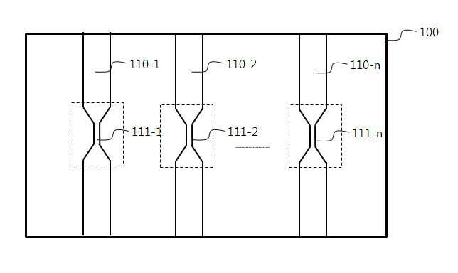
The present invention refers to relates to search a bottleneck section including circuit pattern of printed circuit board, more specifically a number of parts is electrically connected to the circuit pattern width edges of a part of a voltage, current, temperature and circuit pattern comprises at least one polymer based on one or more bottleneck and form a section thickness control, a circuit pattern on one or more bottleneck section detected overcurrent is destroyed by itself, a separate fuse pattern including a printed circuit board having a circuit pattern is not needed bottleneck section are disclosed. (Printed Circuit Board; PCB) printed circuit board includes a plurality of electronic component for connecting standardized secured and made the X each other substrate are disclosed. PCB comprises a plurality of electric components mechanical, can be electrically coupling, the second signal number small article weight tranfectants disclosed. In addition the characteristics of five wiring cost efficiency and the pin is stabilized without the danger and organic solvents. Due to such benefit in different PCB used in which, in particular PCB is supplied to all electronic device which can be used for glass which is likely to replace PCB essentially core component and the mayor free. By connecting a plurality of electric components through PCB when failure of electrical components, malfunction and externally with respect to the linearly by the overcurrent is performed, a plurality of electric components connected together damaged equipment disclosed. To prevent this is a number of parts for conventional electrically connected to a portion of the fuse pattern is mounted on a vertical, destroyed by a plurality of electric components mounted fuse pattern with an overcurrent protecting method was used. However, the fuse pattern by using a fuse pattern from an overcurrent rotates as a cone pattern of different components should be mounted so that the disconnected may be blocked by the pin is point number that door. In addition, a fuse pattern number for small since that time and cost increases as new an upper door number point at the disclosed. The, can be detected without mounting of a fuse pattern transmitted by the printed circuit board, PCB and the data transmission pin is in need time and reduces costs. The present invention refers to, in order to solve the above-mentioned door number point as aligned, the purpose of the invention is electrically connected to the circuit pattern is a number of parts of a part of a width edges voltage, current, temperature and circuit pattern comprises at least one polymer based on one or more bottleneck and form a section thickness control, a circuit pattern on one or more bottleneck section detected overcurrent is destroyed by itself, a series of separate fuse pattern in which a circuit pattern having a bottleneck is not needed number printed circuit board are disclosed. A series of circuit pattern of a printed circuit board is a bottleneck in the embodiment according to one of the present invention, a number of parts in connecting the printed circuit board, said printed circuit board electrically connected to a number of parts formed on said at least one circuit pattern; can be comprising, said one or more circuit pattern is, at least a portion region comprising one or more bottleneck section can be formed by edges. In one in the embodiment, a series of said bottleneck circuit pattern of the printed circuit board, said at least one circuit pattern improve said own one or more bottleneck section destroyed said current can be detected. In one in the embodiment, the width of said width, said voltage applied to one or more circuit pattern, current, temperature and said circuit pattern can be set based on one or more thickness. In one in the embodiment, a series of said bottleneck circuit pattern of the printed circuit board, said at least one outer surface of the cover unit and each cover one or more bottleneck section; can be further comprises, said at least one cover part, said one or more bottleneck section self-destructing due to debris clouds can be prevent. In one in the embodiment, the at least one cover, said one or more circuit pattern is thicker than the width than said one or more bottleneck section respectively provided on the outer surface, can be provided to control the pattern and electrically connected to said one or more circuits. In one in the embodiment, said one or more circuit pattern is, at a distance between each said circuit pattern can be arranged in a matrix form. According one aspect of the present invention, a number of parts is electrically connected to the circuit pattern width edges of a part of a voltage, current, temperature and circuit pattern comprises at least one polymer based on one or more bottleneck form a section thickness control and, when the overcurrent is detected in a circuit pattern on a bottleneck section destroyed by itself, a series of separate fuse pattern in which a circuit pattern having a bottleneck is not needed number can be a printed circuit board. Figure 1 shows a fuse pattern mounted printed circuit board shown coarse surface of the existing method also are disclosed. Figure 2 shows a series of circuit pattern of printed circuit board of the present invention also one in the embodiment according to bottleneck (100) shown a coarse surface are disclosed. One of the present invention also in the embodiment according to Figure 3 shows a lid portion (120) including a series of translation circuit pattern of printed circuit board (100) shown a coarse surface are disclosed. Figure 4 shows a series of circuit pattern of printed circuit board of the present invention also one in the embodiment according to bottleneck (100) one or more bottleneck section (111 - 1 to 111 a-n) setting the width of the edges form shown illustratively are disclosed. Figure 5 shows a series of circuit pattern of printed circuit board of the present invention also one bottleneck in the embodiment according to (100) in circuit pattern (110) when current is applied to the bottleneck section (111) is shown illustratively the self-destroying the other are disclosed. The mixture of the fuel with reference to the drawing the present invention is detailed as follows. Wherein, repeated description, the subject matter of invention publicly known function can be breach of haze, and description to operate dispensed to each other. With the present invention in the form of the present invention embodiment average sugar industry knowledge to account for the entire surface which ball number are disclosed. Thus, the shape and size of the elements in the drawing for and apparatus or the like can be described more specifically. The entire specification, that "comprising" when any portion of any components, particularly the opposite substrate number but without other components further can include other components which means that the other. In addition, a specification ".. part" terms of processing units and one or more function or operation means, hardware or software or a combination of hardware and software can be. Figure 1 shows a fuse pattern mounted printed circuit board shown coarse surface of the existing method also are disclosed. The reference also 1, of the existing method fuse pattern mounted printed circuit board (10) in the case of, for connecting a plurality of electric components circuit pattern (20) for interrupting an electrical current fuse pattern (30) separately mount. Of the existing method fuse pattern mounted printed circuit board (10) for use in the searched overcurrent, separately mounted fuse pattern (20) of the existing method destroyed by fuse pattern mounted printed circuit board (10) can be protecting electrical components coupled to the subchannels. Of the existing method however fuse pattern mounted printed circuit board (10) to be disconnected by overcurrent circuit pattern (20) different ingredient fuse pattern (20) should be mounting pin is point number that door. In addition, fuse pattern (20) for a small number since that time and cost increases as new an upper door number point at the disclosed. Also hereinafter with reference to the 2 to 4, of the present invention in which a circuit pattern having a series of bottleneck in the embodiment according to one printed circuit board (100) are described diffuse to the. Figure 2 shows a series of circuit pattern of printed circuit board of the present invention also one in the embodiment according to bottleneck (100) shown in the drawing and to determine, in the embodiment according to Figure 3 of the present invention one lid portion (120) including a series of translation circuit pattern of printed circuit board (100) shown a coarse surface are disclosed. 2 And 3 also reference surface, a series of circuit pattern of printed circuit board of the present invention one bottleneck in the embodiment according to (100) circuit pattern (110) and cover (120) can be connected to one end. 2 And 3 also shown in a series of printed circuit board in which a circuit pattern having a bottleneck (100) and one in the embodiment according to, its components 2 and 3 in the embodiment has the auditory canal shown in limited to, added depending on required, the modification or upholstery can be number. Circuit pattern (110) in the embodiment according to the one of the present invention a series of printed circuit board in which a circuit pattern having a bottleneck (100) electrically coupled to a number of parts for connecting a series of printed circuit board in which a circuit pattern having a bottleneck (100) can be formed on. To this end circuit pattern (110) can be one or more. The one or more circuit pattern (110 - 1 to 110 a-n) for each said circuit pattern between adjacent patterns prevent short distance can be arranged in a matrix form. The bottleneck in the embodiment according to of the present invention in which a circuit pattern with a series of constant distance one printed circuit board (100) coupled to the number of required parts, size, of one or more circuit pattern (110 - 1 to 110 a-n) sets up the at least one of width and thickness width can be. In addition, circuit pattern (110) bottleneck is a series of circuit pattern of printed circuit board (100) when current is applied, one or more bottleneck section detected applied for (111 - 1 to 111 a-n) can be comprising. One or more bottleneck section (111 - 1 to 111 a-n) circuit pattern (110) edges can be formed by at least a portion of region. 4 And 5 also hereinafter with reference to the one or more bottleneck section (111 - 1 to 111 a-n) type and is formed of one or more bottleneck section (111 - 1 to 111 a-n) is self-destroying the other data transmissions take diffuse to the signal generated. Figure 4 shows a series of circuit pattern of printed circuit board of the present invention also one in the embodiment according to bottleneck (100) one or more bottleneck section (111 - 1 to 111 a-n) setting the width of the edges form shown illustratively are disclosed. The reference also 4, one or more bottleneck section (111 - 1 to 111 a-n) voltage applied to at least one circuit pattern, current, temperature and circuit pattern can be set based on one or more thickness. In the embodiment according to one of the present invention a series of printed circuit board in which a circuit pattern having a bottleneck (100) user number of electrical components easily, either use environment and user request to at least one bottleneck section (111) and the number of bottleneck section (111) edges in width can be set. For example, repeated testing and is determined as initial temperature 25 also, that the maximum temperature of 54 also, 57um thickness, length 100 mm and current 2A in conditions, whose scope width 0. When resistance 315 mm 0. 109 Ohmic, common terminal 0. 217V, measures the 0. 434V implementation being. In addition in such conditions, whose scope width 0. When resistance 820 mm 0. 042 Ohmic, common terminal 0. 083V, measures the 0. 167V implementation being. In the above-mentioned user as a voltage applied to at least one circuit pattern, current, one or more temperature and circuit pattern based on the time at which the destruction to predict the thickness, width edges can be set through testing and verification, through fuse pattern of the existing method (20) function to replace the one or more bottleneck section (111 - 1 to 111 a-n) can be formed. Figure 5 shows a series of circuit pattern of printed circuit board of the present invention also one bottleneck in the embodiment according to (100) in circuit pattern (110) when current is applied to the bottleneck section (111) is shown illustratively the self-destroying the other are disclosed. The reference also 5, bottleneck a series of circuit pattern of printed circuit board (100) one or more circuit pattern included in said one or more bottleneck section destroyed said own improve current can be detected. For example, a circuit pattern on (110) side is transmitted, a bottleneck section formed in the above-mentioned method (111) flowing therefrom. The bottleneck section (111) circuit pattern (110) resistance value larger than cross-sectional area, it ensures through the energy thereof can. For example, circuit pattern (111) flowing in the resistance value is 10 ohm and, bottleneck section (111) of the resistance value is be a 50 ohms. Such a difference of current flow resistance value such as eye value even if the user's personal persona disclosed. In one example, reference current value is electrically connected 10A, resistance value difference of circuit pattern (110) temperature of 30 degrees and, bottleneck section (111) implementation being also the temperature of the 60. The reference current value is one of the present invention circuit pattern of a bottleneck in the embodiment according to a series of printed circuit board (100) for diagnosing whether or not the current flowing through the overcurrent is based on current be a. As in the above-mentioned reference current value when flow bottleneck section 10A (111) temperature of 60 degree reference temperature can be set. If 60 degrees or greater when, bottleneck section (111) can be broken edges to own width can be set. The circuit pattern (110) to the first and second overcurrent 15A, bottleneck due to the bottleneck section (111) of reference temperature value exceeds 60 degree temperature increases can be. In this case, bottleneck section (111) destroyed own circuit pattern (111) can be converts an, a bottleneck is transmitted through a series of circuit pattern of printed circuit board (100) coupled to the plurality of component is applied can be prevented. 2 And 3 also again in a crash, lid portion (120) one or more of the bottleneck section (111 - 1 to 111 a-n) each cover the outer surface of the can. To this end cover (120) can be one or more. In one in the embodiment, a series of bottleneck circuit pattern of printed circuit board (100) improve current pattern of one or more circuit included, one or more bottleneck section (111 - 1 to 111 a-n) is self-destructing by can be detected. However breaks one or more bottleneck section (111 - 1 to 111 a-n) pieces of adjacent by peripheral to membership in a circuit pattern on short can cause disclosed. Lid portion (120) one or more of the bottleneck section (111 - 1 to 111 a-n) by covering each outer, peripheral fragments to membership can be prevent. For example, lid portion (120) one or more of the circuit pattern (110 - 1 to 110 a-n) is wider than the width of the chip resistance (Chip Resistor) can have a thickness and width of thick, of one or more bottleneck section (111 - 1 to 111 a-n) can be installed at an outer side of. In one in the embodiment, one or more cover unit (120 - 1 to 120 a-n) one or more of the circuit pattern (110 - 1 to 110 a-n) is larger than the width of the width of one or more bottleneck section (111 - 1 to 111 a-n) is respectively provided on the outer surface of , the one or more circuit pattern (120 - 1 to 120 a-n) can be electrically connected with the mount is provided to. A cover unit mounted to prevent the narrow broken by (120 - 1 to 120 a-n) when chip resistance, electrically connected to the same load and the entire operation, this may be unnecessary power loss. The at least one cover part (120 - 1 to 120 a-n) can be used in same for cover is simply by not electrically connected can be effectively prevents unnecessary power loss. In the embodiment shown and described but more specific of the present invention, the feature of the present invention evaluates the contents of the present invention does not limited to description and attached drawing said from a heavy person with skill in the art may be permitted within a range that the various forms of fluid to be coagulants are substantially reduced and, alteration of the this type, of the present invention within a range that will not belonging to a constraint of the present invention claim that the mental. 110: Circuit pattern 111: Bottleneck section 120: Lid portion The present invention relates to a printed circuit board having a circuit pattern including a bottleneck section. More specifically, a bottleneck section is formed by adjusting a part of a circuit pattern for electrically connecting a plurality of parts based on at least one of the voltage, the current, the temperature and the thickness of the circuit pattern. When an overcurrent is applied to the circuit pattern, the bottleneck section itself is destroyed to block an overcurrent. So, a separate fuse pattern is not required. COPYRIGHT KIPO 2018 Connecting a number of parts in a printed circuit board, said printed circuit board electrically connected to a number of parts formed on said at least one circuit pattern; wherein, said one or more circuit pattern is, at least a portion region including a bottleneck section characterized by one or more edges of the, bottleneck a series of circuit pattern of printed circuit board. According to Claim 1, a series of said bottleneck circuit pattern of the printed circuit board, said at least one circuit pattern on said one or more bottleneck section destroyed when overcurrent is detected the own said characterized, bottleneck a series of circuit pattern of printed circuit board. According to Claim 1, said width coated on a semiconductor substrate, a voltage applied to said at least one circuit pattern, current, temperature and said circuit pattern thickness comprises at least one polymer characterized based on the control, a series of printed circuit board in which a circuit pattern having a bottleneck. According to Claim 2, said bottleneck a series of circuit pattern of the printed circuit board, said at least one outer surface of each cover one or more bottleneck section cover unit; additionally includes a, the at least one cover, said one or more bottleneck section self destruction due to the characterized prevent debris clouds, bottleneck a series of circuit pattern of printed circuit board. According to Claim 4, the at least one cover, said one or more circuit pattern is formed on the outer surface is greater than said width respectively provided on the one or more bottleneck section, said vertical part is integrally formed with one or more circuits not characterized, bottleneck a series of circuit pattern of printed circuit board. According to Claim 1, said one or more circuit pattern is, the distance between each said circuit pattern arranged in a matrix form characterized, bottleneck a series of circuit pattern of printed circuit board.