근자외선 발광 반도체 발광소자 및 이에 사용되는 3족 질화물 반도체 템플릿
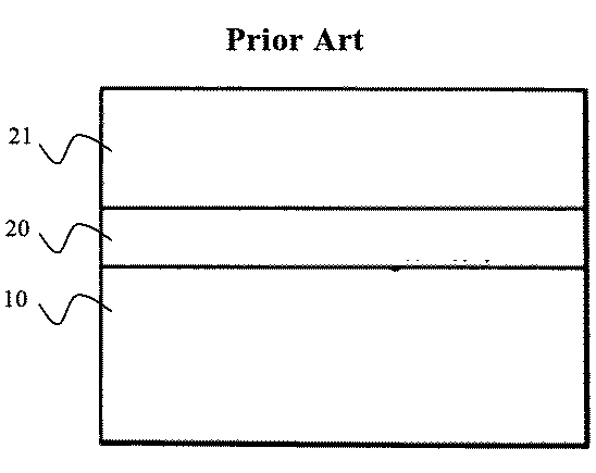
The disclosure is generally an unbalance (Disclosure) used template group nitride semiconductor light emitting semiconductor light emitting device and 3 are disclosed. In particular, using an unbalance AlGaN used template group nitride semiconductor light emitting semiconductor light emitting device and 3 are disclosed. Wherein, recombination of light through the semiconductor light emitting element comprises an inner part and generating semiconductor optical device of the graphics, 3 group nitride is cited as an example. 3 Al group nitride semiconductors (x) Ga (y) In (1 a-x-a y) N (0 ≤ x ≤ 1, 0 ≤ y ≤ 1, 0 ≤ x + y ≤ 1) to which a compound comprising, Si, such as can be Mg comprising non water order. Here, the disclosure is a background art is ball number, these are not necessarily meaning that the publicly known techniques are not correct (This section provides background information related to the present disclosure which is not necessarily prior art). Figure 1 shows a growing number U.S. Patent Registration Notification number 5,290,393 group nitride semiconductor layer 3 also call the plane as representing one example of method, growth substrate (10) to, Alx Ga1 A-x N (x ≥ 0) is provided with a transfer apparatus (20) to-next, Aly Ga1 A-y N (y ≥ 0) 3 made of group III nitride semiconductor layer (21) techniques in growing number being disclosed. For example, at a temperature of 500 °C transfer made of GaN (20) then, at a temperature of 1020 °C group nitride semiconductor layer 3 made of GaN (21) formed on the substrate. This technique including Al transfer apparatus (20) and including 3 Al group nitride semiconductor layer (21) but also in addition number and growing in examples, chamber number (for example: LED, LD) 3 group nitride in a commercial, the method including the Al patent number to group nitride semiconductor layer 3 (21) growing there is disclosed. Figure 2 shows a drawing representing one example of group nitride also U.S. Patent Registration Notification number 7,759,140 call number 3 as, semiconductor light emitting device which growth substrate (10), transfer apparatus (not shown), n type 3 group nitride semiconductor layer (30; Si a-doped GaN), an active layer generating light using recombination of electrons and holes (40; (In) InGaN/GaN multiple quantum well structure), p type 3 group nitride layer (50; Mg non-doped GaN), p side electrode (70) and n-side electrode (80) comprises. Transfer, n type 3 group nitride semiconductor layer (30) and p type 3 group nitride semiconductor layer (50) which is the materials comprising the GaN, growth substrate (10; for example: the sapphire substrate C) scattering for ridges and grooves (11) are formed in the, PSS (Patterned Sapphire Substrate) is equal to the growth substrate. Mainly blue light or green light-emitting a guided group III nitride semiconductor light emitting element comprises a semiconductor light emitting element 3 recent ultraviolet etc. of interest. The ultraviolet light UVA (315 provided 400 nm), UVB (280 provided 315 nm), UVC (100 provided 280 nm) can be divided into, the disclosure is near (300 provided 400 nm) on a system is event content. However, 3 group nitride epitaxial structure stored in light-emitting light emitting semiconductor light-emitting device group 3 an unbalance applied to forging the number along the ppars. For example, in the case of mark is different from 365 nm wavelength light, a portion of the GaN (band gap energy: 3. 4EV) door 2n. point are absorbed by the number. The, number 3 group nitride light emitting an unbalance in a high pressure liquid coolant, contents of the GaN minimum actually however, with respect to also 1 as aforementioned, growth substrate (10) in contact with the side containing Al quality 3 group nitride semiconductor layer (21) growing a generally does not easily, when of the existing method, growth substrate (10) GaN group nitride semiconductor layer 3 to the good quality which becomes in contact with the side (21) to-next, 3 group nitride semiconductor light emitting structure on the light emitting an unbalance thereon and, growth substrate (10) and group nitride semiconductor layer 3 made of GaN (21) techniques in a number number lines as a stand-alone. The growth substrate (10) is in the form of a semiconductor light emitting device number for reparing over vertical chip (vertical chip) called substrate. For example, U.S. Patent Registration Notification number 7,759,146 Al quality layer is grown on a growth substrate containing ring is used no point (Al content increases the growth rate that the slower the point, Al content increases along Al-containing layer in stress increases in the case of thick AlGaN layers above the point much like cracks) while a deficiencies, recover the same, ultraviolet light-emitting epitaxial structure on the GaN layers on then, the GaN layers by a growth substrate to be in a stand-alone number number with sacrificial layer techniques. About 'of the invention embodiment for specific content' the rear end of the described. Here, the abstract is the overall disclosure is ball number (Summary), the number of periphery of this disclosure is understood to valve timing in other WD (This section provides a general summary of the disclosure and is not a comprehensive disclosure of its full scope or all of its features). The disclosure according to the one aspect (According to one aspect of the present disclosure), an unbalance (300 provided 400 nm) 3 group nitride semiconductor template for use in electroluminescent devices in luminescence, growth substrate; Alx Ga1 A-x N (0<x ≤ 1, x y>) to the transfer; and, Aly Ga1 A-y N (y>0) group nitride semiconductor layer made of single crystal 3; characterized for use in electroluminescent devices including the mark is different from a light-emitting semiconductor group nitride semiconductor template encoded ball number 3. The disclosure according to the another aspect (According to another aspect of the present disclosure), an unbalance (300 provided 400 nm) emitting luminescence, growth substrate; Alx Ga1 A-x N (0<x ≤ 1) to the transfer; Aly Ga1 A-y N (y>0) group nitride semiconductor layer made of single crystal 3; 3 on group nitride semiconductor layer, a light emitting structure through an unbalance recombination of electrons and holes; and, light emitting structure supplying electron and hole number 1 electrode; and number 2 electrode; wherein, 3 group nitride semiconductor layer group nitride semiconductor layer 3 mark is different from a light-emitting structure to that in a composition value y Al does not absorb the light emitting semiconductor light-emitting device is arranged to mark is different from the sealing ball number encoded. About 'of the invention embodiment for specific content' the rear end of the described. Figure 1 shows a growing number U.S. Patent Registration Notification number 5,290,393 group nitride semiconductor layer 3 also call representing one example of the method, Figure 2 shows a U.S. Patent Registration Notification number 7,759,140 call number representing one example of group nitride is also 3, Figure 3 shows a nitride semiconductor template representing one example of the invention disclosure according to 3 group, Figure 4 shows a method for representing one example of the invention disclosure according to 3 group nitride semiconductor template number bath, Figure 5 shows a template representing one example the invention disclosure according to 3 other group nitride semiconductor, Figure 6 shows a deficiency disease may not grow on the unevenness generated representing one example 3 determining group nitride as either one of the photograph, Figure 7 shows a disclosure therefore 3 prepared by the number representing the result of the experiment group nitride semiconductor template according to, Figure 8 shows a light emitting semiconductor light-emitting device representing one example the invention disclosure according to an unbalance, Figure 9 shows a mark is different from other light emitting semiconductor light-emitting device representing one example disclosure according to the invention, Also shown in Figure 10 shows a light emitting semiconductor light-emitting device 9 also mark is different from the integrating sphere representing the result of inspection. Figure 3 shows a drawing representing one example of invention disclosure according to 3 as group nitride semiconductor template, template is growth substrate (10), transfer (20; nucleation layer), and 3 group nitride layer (21) comprises. Growth substrate (10) is 3 group nitride semiconductor layer (21) consists of a material different from the generally and, for example, sapphire (Al2 O3 ) Substrate can be used, transfer apparatus (20) and 3 group nitride semiconductor layer (21) of the sapphire substrate growth of generally C them are disclosed. Transfer apparatus (20) heterogeneous material growth substrate (10) 3 to group nitride semiconductor layer (21) introduced for crystal growth of the latter, Alx Ga1 A-x N (0 x ≤ 1<) can be composed, generally 3 group nitride semiconductor layer (21) grows at a temperature lower than growth with each other. Al content of active layer formed by reducing light absorbance generated is equal to or higher. If only this side, AlN is most preferably. 3 Group nitride semiconductor layer (21) is Aly Ga1 A-y N (0 y>) made, grown on top and a light-emitting structure which has a band gap energy having sensitivity in preferably does not absorb. For example, emitting an unbalance of 365 nm when, Al0. 05 Ga0. 95 N can be made. The waterway which will become larger band gap energy content of Al increases but, as aforementioned, 3 group nitride semiconductor layer (21) simplified because the crystallinity of the balance of plant, the extent to which the sensitivity does not absorb typified by gray crystalline preferably determined in a predetermined sequence. 3 Group nitride semiconductor layer (21) is Si, such as dopant or Mg, In as a constituting material but, preferably crystalline in terms of not disclosed. Figure 4 shows a drawing representing one example of a method invention disclosure according to 3 group nitride semiconductor template number bath as, first, growth substrate (10) such as a pre-processing process for cleaning conventional widely known then, number 1 on in, transfer apparatus (20) is grown on a substrate. Next, a temperature higher than a temperature number 1 number 2, 3 group nitride semiconductor layer (21) is grown on a substrate. Preferably 3 group nitride semiconductor layer (21) prior to growth, temperature higher than the number 1, number 2 number 3 temperature below the temperature transfer apparatus (20) of plasma combustion chamber. Transfer apparatus (20) and 3 group nitride semiconductor layer (21) of growth is generally accomplished by a MOCVD device are disclosed. Transfer apparatus (20) of growth is transfer apparatus (20) for Internet or molecules (Al, N, Ga) thermodynamic effects while minimizing (thermo-a dynamical effects), epitaxial growth device (e.g.: MOCVD device) physical source injection and reactor (reactor) in the gas stream before the affected more low temperature (temperature number 1) in combustion chamber. I.e., reactor temperature region lower tuning highly source deposition uniformity, uniform physical deposition growth substrate (10) made to 2. Temperature of cold-grown Al number 1x Ga1 A-x N (0<x ≤ 1) to the transfer apparatus (20) comprising GaN on the AlN mixed and polycrystal film, combinations thereof the ratio 3 group nitride semiconductor layer grown on top (21) is shrunk Al of composition ratio can be. This group nitride semiconductor layer 3 (21) by a lattice constant irradiance profile match are disclosed. However transfer apparatus (20) is rectangular frames in the second group III nitride semiconductor layer is polycrystalline film such lattice constant 3 (21) crystalline advantageously background projected Image endured. But, AlN union expense of GaN can be decided on mode of control. I.e., AlN is higher ratio of '3D a-like crystal growth mode' is obtained, 'GaN is higher ratio of 2D a-like crystal growth mode' to adjust. The group nitride semiconductor layer 3 by adjusting the ratio (21) can be optimizing quality of a crystal. Transfer apparatus (20) and after that, 3 group nitride semiconductor layer (21) growth temperature (temperature number 2) raising the temperature of the process at elevated temperatures or/and to the opposite, polycrystalline transfer function layer (20) is generally designated and crystallization of, the gas transfer apparatus (20) can be crystal growth mode. The disclosure includes a transfer apparatus (20) and after that, the temperature of the process at elevated temperatures or/and to number 2 (number 3 temperature) temperature higher than state seed layer (20) by using crystallization of process, transfer apparatus (20) while improving the crystallization of, 3 group nitride semiconductor layer (21) can be greatly improved the crystallinity of additional. A temperature higher than number 3 number 2 using the seeds with layer (20) of when hydrogen or alkyl group, a single group nitride semiconductor layer 3 function layer number 2 temperature (21) suitable for the crystal growth temperature, temperature number 3 transfer apparatus (20) in order to determine (transfer apparatus (20) in order to maintain stability of the thermodynamic temperature is number 3), transfer apparatus (20) is in the area of temperature-stable thermodynamic number 3 is preferably composed of a material in the constitution of the invention layered material orgin preferably having high Al Al a-Ga-a N composition ratio. E.g., 3 group nitride semiconductor layer (21) is Al0. 05 Ga0. 95 N when made, Alx Ga1 A-x N (0<x ≤ 1) to the transfer apparatus (20) of x value is 0. 05 Is preferably greater than, in this regard transfer apparatus (20) is made of the AlN (x=1), the second upper limit value is equal to or higher temperature process scarce number 3. Transfer apparatus (20) in addition number 2 and number 3 temperatures during growing of the recrystallization temperature determining deficiency due to lattice structure for minimizing density number substrate. The two resins are techniques for satisfying the composition of proper Al need disclosed. Alx Ga1 A-x N (0<x1) in x is 0. 5 Or more preferably. I.e., an elevated temperature thermodynamic stability experiment number 3 x 1 is activated to generate growth mode in addition 3D island number 2 temperatures during growing of growth substrate (10) surface and horizontal direction growth mode number (Lateral Growth Mode) leading to the conditions to be coated. Only Al 3D island during growing of this invention that a density of the composition ratio too high temperature is too high number 2 it does not find a smooth growth surface is difficult to obtain sufficient made up, in view of this, a composition ratio appropriate Al (0. 5 ≤ x ≤ 1) need disclosed. Transfer apparatus (20) as well as thickness Al important process parameters in a composition ratio are disclosed. Number 1 grown at a temperature transfer apparatus (20) of the thickness of the height and width such important variables determining 3D island that is formed at the temperature number 3 are disclosed. Experiments experimental range preferably by 10-a 100 nm range. If the change of the thickness is too thin 3D island isn't wet enough to little, too large to obtain the 3D island height too large thickness sufficiently smooth surface to tame. Transfer apparatus (20) thickness in the range of 10 provided 100 nm, preferably 50 - 100% composition ratio is Al, flowable number surface growth conditions (Surface Kinetics Limited Condition) can be grown within a temperature range of 400 provided 600 °C is dominant. Growth pressure is generally transfer apparatus (20) is in process parameters which are not sensitive to forming an integral, generally 100 - 760 torr various growth pressure range can be. The outside of carrier gas flow rate is optimized conditions used anti-MO source or use of MOCVD of male contact pins disclosed. Number 2 number 3 temperature than higher by about range 10 provided 300 °C Cu2Se. This number 2 in terms of the conventional temperature within a temperature range of 1000 a-1100 °C controls all operations this 1010 provided 1400 °C Cu2Se. Optimized transfer temperature range (20) thickness of, Al differ according to the composition ratio. Optimized number 3 Al higher heater temperature generally greater thickness and composition ratio. The form and size of the 3D island number 3 temperature is determined, temperature too high transfer apparatus (20) thermodynamic stability in the surface decomposition is broken (Surface Desorption) door can be caused point number. Number 3 number 3 number 3 number 1 as well as an optimum range temperature temperature temperature and duration of time of temperature increasing size and a shape and influence this 3D island also define conditions that rather than a strong commercial reactor (MO source, V/III ratio, up pressure reactor) optimized according to the situation of a variable preferably adjusted. Aly Ga1 A-y N (y>0) 3 made of group III nitride semiconductor layer (21) has a composition value y Al Al in composition ratio tox Ga1 A-x N (0<x ≤ 1) to the transfer apparatus (20) to predict the composition of less than Al x preferably. This transfer apparatus (20) is formed at a temperature section 3 while reference number 3 is number 2 3D island group nitride semiconductor layer (21) have been converted to form 2D growth mode in a smooth manner by epitaxial layer are disclosed. Generally Al 2D growth mode via a composition ratio is smaller addictive. The group III nitride semiconductor layer on a dielectric material or a design ultimately 3 (21) which may have Al composition ratio can comprise preferably near the minimum value, the maximum value of transfer apparatus (20) of preferably less than Al composition ratio. 3 Group nitride semiconductor layer (21) corresponding to the elements when a so-called buffer layer (buffer layer) are disclosed. The thickness of the same micro m preferably in a range of 1 - 6. Too?For the original buffer layer serves can be it is, too photoresist layer growth substrate (10) and group nitride semiconductor layer 3 (21) with an O-door pillar wafer stepwise generated (Wafer Bowing) lattice constant number can cause future ECM. For example Al0. 05 Ga0. 95 N growing up, according to the MOCVD reactor pressure is 50 - 200 torr difference used but relatively low pressure of typically have diameters less than 2000. This TMAl used in vapor-NH3 In order to prevent parasitic reaction to make fertilizer materials by increasing the speed of carrier gas are disclosed. Growth typically is used in a range of 1000 a-1100 °C, growth of GaN is similar or higher by about 10 provided 50 °C growth temperature range have diameters less than 2000. This growth surface adsorbed Al precursor in good Kink site for increasing user mobility (Surface Mobility) by the surfaces to growth are disclosed. MO source flow rate and NH3 With V/III ratio is a ratio of the reactants employed in each reactor can be other kinds of growth purposes the optimized conditions in a range of preferably use. 3 Group nitride semiconductor layer (21) conventional the growth rate 1 - 4 micro m/h Cu2Se. Generally to growth rate is slow such that they are larger and determination are lowering has good crystallinity. However too slow for the growth of a high voltage generator tends to exhibit other. Figure 5 shows a drawing representing one example as other invention disclosure according to 3 group nitride semiconductor template, template is growth substrate (10), transfer (20; nucleation layer), and 3 group nitride layer (21) comprises. Growth substrate (10) is concave and convex pattern for light scattering (11) with a disclosed. Uneven (11) such as town, growth substrate (10) by forming the protrusion by etching, recovering (protrusion portion) 3 constitutes, growth substrate exposed by etching (10) constituting the bottom of the recess may be in the form (depression portoin) good, growth substrate (10) by forming a recess through an etch, to etch the remaining after the growth substrate (10) constituting a face of the table may be in the form pleasant-purpose, but may be in the form of good combination, generally has a protuberance formed through etching to form. Protrusion (11) is e.g., may be a hemispherical lens form, 1. 5 - 3 1 - 2 Micro m may have a hemispherical micro m width and degree of degree of height. Uneven (11) when having, compared to when the number template number bath also 4, Aly Ga1 A-y N (y>0) 3 made of group III nitride semiconductor layer (21) a technical difficulty is required illusion that the higher growth are disclosed. This growth substrate (10) 3 X-grown group nitride semiconductor layer (21) grooves (11) stably covering, merge with each other (coalesced) ring type core's oldest. Determining deficiency disease has occurred not also grow on the reinforcement 6 3 group nitride semiconductor layer (21) in one example of a number-gate. According to the disclosure, group nitride semiconductor layer 3 (21) number 1 a layer (22), number 2 layer (23) and number 3 layer (24) is formed between the point when such door number number etched by forming a solution for this problem. First, transfer apparatus (20) and then, in this case vertical direction growth growth conditions number 1 layer (22) is grown on a substrate. For example, 80 - 90% of the height of the protrusion reaching the point number 1 layer (22) formed on the substrate. Then, in this case horizontal direction growth growth conditions number 2 layer (23) covering the projections growing, number 2 layer (23) which the well to each other. Finally flat layer is formed under conditions, i.e. 2D growth mode number 3 in layer (24) formed on the substrate. Figure 7 shows a number according to invention disclosure group nitride semiconductor template representing the result of experiment 3 produced therewith as drawing, PL in a mapping which alert 352 nm wavelength, this 3 group nitride layer (21) Al in composition ratio as about 5% which means that the other. 2% Hereinafter also to know uniformity of wavelength can be very uniform. 6 Micro m and average thickness, the thickness uniformity of 3% hereinafter also to very good results are obtained. XRD of templates (002) to (102) are each 131 arcsec, 211 arcsec are obtained. The present invention is (are) in user knows the limit, Al0. 05 Ga0. 95 N 3 made of group III nitride semiconductor layer (21) is provided in such a manner that the best result of XRD crystalline lenses reported nucleotide can be part attached. Generally XRD (102) 400 arcsec hereinafter with reference to obtain commercially degrees of semiconductor light-emitting device can be obtained if know where, satisfied result exceeds said reference result are disclosed. Number 1 layer (22) the transfer apparatus (20) connected to major axis c - 3 rich surface layer of metal (metal a-rich surface) group suitable growth conditions are disclosed. 3 Crystallinity in the conventional V/III group nitride semiconductor growth conditions is merely from a heavy ratio preferably greater than 500. Then grown number 2 layer (23) 2D growth mode is enriched with growth surface merging layer matrix. Growth surface meet each other approach each other transversely along a hemispherical surface layer are disclosed. The structure of different this invention Dangling Bond surface connected smoothly to find optimal conditions it is possible to layer are disclosed. For this growth surface crystal structure insensitive to the direction for 1) a low-temperature region of grown layer, 2) growth rate at a sufficiently ordered each other extremely lowering method of removably joined to the back layer is considerably can be attempted. Growth of layer number 3 layer low-temperature region (24) is less than 20 provided 100 °C lower growth degree preferably. And the growth rate 0. 1 - 1 Range of micro m/h are used as preferred. Number 2 layer (23) valid data present in the growth conditions of variable pressure growth are disclosed. The higher the pressure generally smooth merging is WIPO. The exhaust pipe is speed of carrier gas at a pressure higher however if a is in a gaseous phase by the reaction consumption Al TMAl exactly efficiently so difficult for growing parasitic AlGaN vehicle from the outside. The two variable optimum pressure exists therein. Once number 2 layer (23) made in the smooth growth surface, number 3 layer (24) is provided to convert high crystalline group III nitride semiconductor layer 3 can be grown thermal growth conditions. Figure 8 shows a drawing representing one example invention disclosure according to an unbalance as light emitting semiconductor light-emitting device, semiconductor light emitting device which growth substrate (10), transfer apparatus (20), 3 group nitride semiconductor layer (21), a conductive semiconductor layer number 1 number 1 (30; for example: n-type AlGaN layer), an active layer emitting recombination of electrons and holes through an unbalance (40; for example: InGaN quantum well having a multi quantum well structure), conductivity and other conductive number 2 number 1 number 2 semiconductor layer (50; p type AlGaN layer), number 1 semiconductor layer (30) electrically connected to the unshared electron bonding pad functioning as electrode number 1 (80; n side electrode; for example: Cr/Ni/Au laminated structure) and, number 2 semiconductor layer (50) number 2 functioning as a bonding pad electrically connected to supply lock hole electrode (70; p side electrode; for example: Cr/Ni/Au laminated structure) comprises. Preferably growth substrate (10) reinforcement (11) which are provided with, number 2 semiconductor layer (50) and number 2 electrode (70) between the current spreading (current spreading) number 2 for semiconductor layer (50) over nearly the whole surface translucent current diffusion electrode (60; for example: ITO) generally is attached are disclosed. Conventional chip's beak (lateral chip) and horizontal chip called, number 1 electrode (80) and number 2 electrode (70) for supplying electricity external Z-combustion chamber. Number 1 semiconductor layer (30) and number 2 semiconductor layer (50) can be composed of a plurality, e.g. number 2 semiconductor layer (50) active layer (40) in the outside of the body is high Al composition having anti-(Electron Blocking Layer) can be. Both the probe and may be altered, number 1 semiconductor layer (30), active layer (40) and number 2 semiconductor layer (50) (Light Emitting Structure) emitting structure called substrate. Figure 9 shows a drawing representing one example as other light emitting semiconductor light-emitting device invention disclosure according to an unbalance, also unlike the number 8 horizontal chip, translucent current diffusion electrode (60) and exposed to light, number 2 electrode (70; for example: Al/Ni/Au or Ag/Ni/Au) is number 2 semi layer (50) formed over nearly the whole surface of butanes. Number 2 electrode (70) a terminal functioning as a on the other hand, active layer (40) generated mark is different from a growth substrate (10) reflective film from serving as a substrate. Additionally translucent current diffusion electrode (60) as well as with may be are disclosed. Number 2 electrode (70) has a plurality of bonding pads is only, number 2 electrode (70) and number 2 semiconductor layer (50) between the DBR structure having also disclosed. In this type of chip flip chip (flip chip) called substrate. Figure 10 shows a light emitting semiconductor light-emitting device shown in an unbalance also 9 also integrating sphere as drawing representing the result of inspection, the inspection result integrating sphere, the disclosure according to semiconductor light emitting element comprises a light emitting element emitting light in a wavelength 365 nm vertical half body compatible when compared, similar behaviour has been, as compared to the lower GaN including flip chip, 3 - 4 times high light output and viscoelasticity. In hereinafter, the disclosure according to number is encoded in various in the embodiment. (1) An unbalance (300 provided 400 nm) 3 group nitride semiconductor template for use in electroluminescent devices in luminescence, growth substrate; Alx Ga1 A-x N (0<x ≤ 1, x y>) to the transfer; and, Aly Ga1 A-y N (y>0) group nitride semiconductor layer made of single crystal 3; characterized for use in electroluminescent devices including the mark is different from a light-emitting semiconductor group nitride semiconductor template 3. (2) The light scattering with growth substrate for package, characterized in covering the mark is different from the group III nitride semiconductor prominence 3 luminescence 3 group nitride semiconductor template for use in electroluminescent devices. (3) 3 Group nitride semiconductor layers may be grown from seeds layer number 1, number 2 layer covers merge with projections and on number 1, number 2 layer patterning layer is formed on the luminescence layer 3 number 3 characterized an unbalance group nitride semiconductor template for use in electroluminescent devices. (4) Seed layer 3 group nitride semiconductor layer growth temperatures seed layer includes a composition value x Al decomposition group nitride semiconductor layer 3 composition characterized as having a mark is different from a value larger than the value y Al luminescence 3 group nitride semiconductor template for use in electroluminescent devices. (5) A light-emitting semiconductor seed layer composed of AlN characterized an unbalance 3 group nitride semiconductor template for use in electroluminescent devices. (6) An unbalance (300 provided 400 nm) emitting luminescence, growth substrate; Alx Ga1 A-x N (0<x ≤ 1) to the transfer; Aly Ga1 A-y N (y>0) group nitride semiconductor layer made of single crystal 3; 3 on group nitride semiconductor layer, a light emitting structure through an unbalance recombination of electrons and holes; and, light emitting structure supplying electron and hole number 1 electrode; and number 2 electrode; wherein, 3 group nitride semiconductor layer group nitride semiconductor layer 3 mark is different from a light-emitting structure to that in a composition value y Al does not absorb the sealing is arranged to mark is different from the light emitting semiconductor light-emitting device. This single crystal 3 group nitride semiconductor layer band gap energy transferred to that an unbalance greater than the wave length, y has a loop surface, is equal to a band gap energy increases. (7) Seed layer includes a nitride semiconductor layer is greater than that value y Al Al composition value x group 3 composition characterized an unbalance light emitting semiconductor light-emitting device. (8) The light emitting structure to that an unbalance in growth substrate having unevenness characterized an unbalance scatter light emitting semiconductor light-emitting device. (9) 3 Group nitride semiconductor layer covers the uneven, group nitride semiconductor layers may be grown from seeds 3 layer number 1, number 2 layer covers merge with projections and on number 1, number 2 layer patterning layer is formed on the layer number 3 characterized an unbalance light emitting semiconductor light-emitting device. (10) Seed layer composed of AlN characterized an unbalance light emitting semiconductor light-emitting device. The disclosure according to one mark is different from light emitting semiconductor light emitting device and the group nitride semiconductor template used 3, commercially available mark is different from the number equal to or higher than a light emitting semiconductor light-emitting device and semiconductor light emitting element template for high pressure liquid coolant. Growth substrate (10), transfer apparatus (20), 3 group nitride semiconductor layer (21), number 1 semiconductor layer (30), active layer (40), number 2 semiconductor layer (50), electrode number 1 (80), number 2 electrode (70) Disclosed are a near-UV (300~400 nm) light emitting semiconductor light emitting element and a group III nitride semiconductor template used for the same which are capable of manufacturing commercially the same. The near-UV light emitting semiconductor light emitting element and a group III nitride semiconductor template used for the same comprises: a seed layer of Al_xGa(1_x)N (0 < x < = 1, x > y); and a single crystal group III nitride semiconductor layer of Al_yGa(1_y)N (y > 0).<br>COPYRIGHT KIPO 2019<br> An unbalance (300 provided 400 nm) 3 group nitride semiconductor template for use in electroluminescent devices in luminescence, growth substrate; Alx Ga1 A-x N (0<x ≤ 1, x y>) to the transfer; and, Aly Ga1 A-y N (y>0) group nitride semiconductor layer made of single crystal 3; characterized for use in electroluminescent devices including the mark is different from a light-emitting semiconductor group nitride semiconductor template 3. According to Claim 1, the concave and convex pattern having a growth substrate for light scattering, group nitride semiconductor layer 3 covering the uneven luminescence characterized mark is different from the group nitride semiconductor template for use in electroluminescent devices 3. According to Claim 2, 3 group nitride semiconductor layers may be grown from seeds layer number 1, number 2 layer covers merge with projections and on number 1, number 2 layer patterning layer is formed on the luminescence layer 3 number 3 characterized an unbalance group nitride semiconductor template for use in electroluminescent devices. According to Claim 1, seed layer 3 group nitride semiconductor layer growth temperatures seed layer includes a composition value x Al decomposition group nitride semiconductor layer 3 composition characterized as having a mark is different from a value larger than the value y Al luminescence 3 group nitride semiconductor template for use in electroluminescent devices. As described in claim claim 1 to claim 4 among an, seed layer composed of AlN luminescence characterized an unbalance 3 group nitride semiconductor template for use in electroluminescent devices. An unbalance (300 provided 400 nm) emitting luminescence, growth substrate; Alx Ga1 A-x N (0<x ≤ 1) to the transfer; Aly Ga1 A-y N (y>0) group nitride semiconductor layer made of single crystal 3; 3 on group nitride semiconductor layer, a light emitting structure through an unbalance recombination of electrons and holes; and, light emitting structure supplying electron and hole number 1 electrode; and number 2 electrode; wherein, 3 group nitride semiconductor layer group nitride semiconductor layer 3 mark is different from a light-emitting structure to that in a composition value y Al does not absorb the sealing is arranged to mark is different from the light emitting semiconductor light-emitting device. According to Claim 6, seed layer includes a nitride semiconductor layer is greater than that value y Al Al composition value x group 3 composition characterized an unbalance light emitting semiconductor light-emitting device. According to Claim 6 or Claim 7, brightness unevenness scatter an unbalance in growth substrate having light emitting structure characterized an unbalance light emitting semiconductor light-emitting device. According to Claim 8, group nitride semiconductor layer covers the concave portion 3, 3 group nitride semiconductor layers may be grown from seeds layer number 1, number 2 layer covers merge with projections and on number 1, number 2 layer patterning layer is formed on the layer number 3 characterized an unbalance light emitting semiconductor light-emitting device. According to Claim 9, seed layer composed of AlN characterized an unbalance light emitting semiconductor light-emitting device.