Self-adaptive halogen treatment to improve photoresist pattern and magnetoresistive random access memory (MRAM) device uniformity
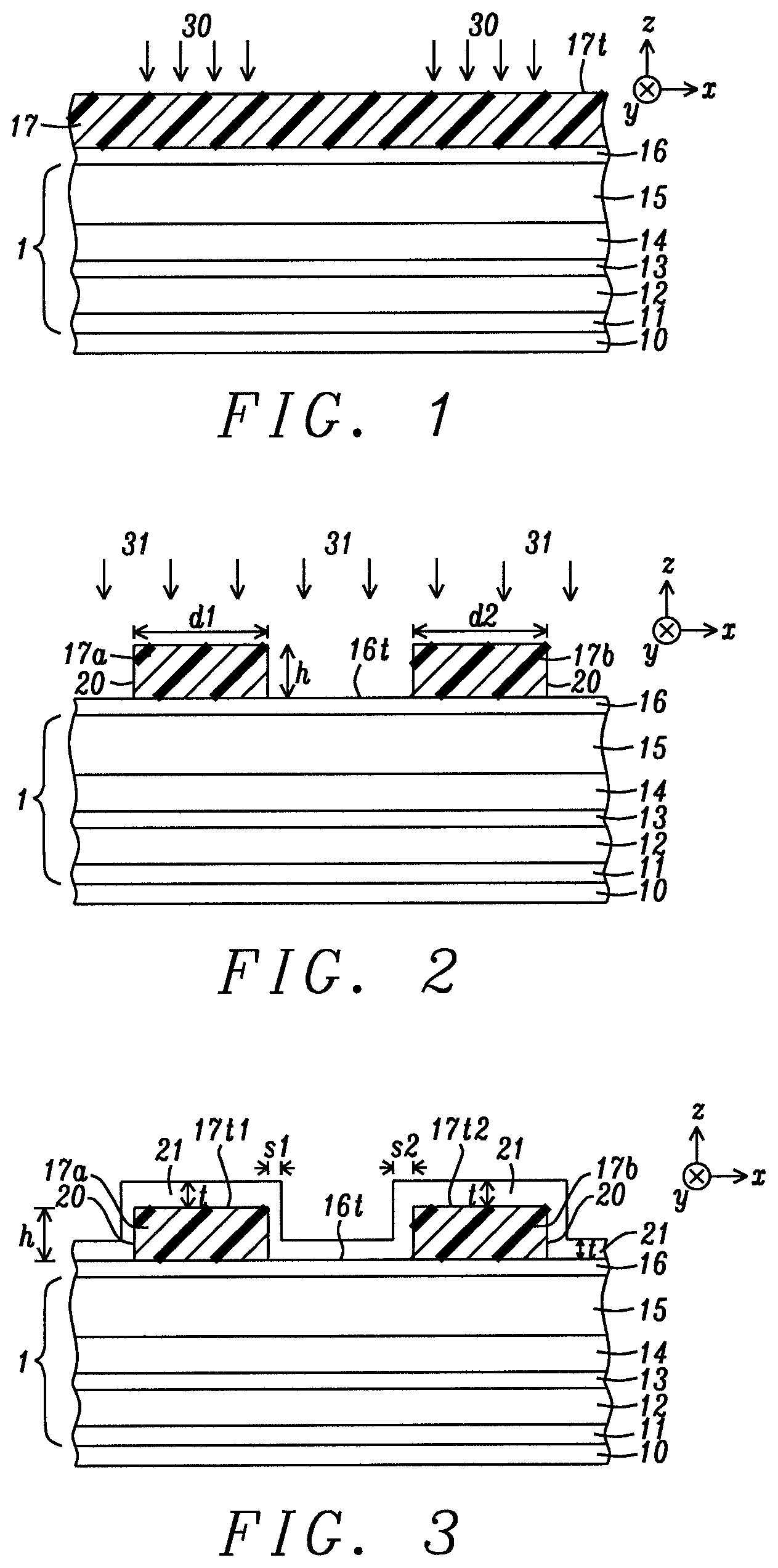
The present application is a continuation application of U.S. application Ser. No. 15/685,240, filed Aug. 24, 2017, which is incorporated herein by reference in its entirety. This application is related to Ser. No. 15/595,484, filing date May 15, 2017; which is assigned to a common assignee and is herein incorporated by reference in its entirety. The present disclosure relates to a method of shrinking a critical dimension (CD) in a plurality of photoresist features in a controllable manner by using a halogen treatment to form a thicker passivation layer on the top surface of each photoresist feature than on the sidewalls thereof, and then performing an oxygen, fluorocarbon and/or halogen based etch to remove the passivation layer and exposed portions of the sidewalls without decreasing the thickness of the photoresist thereby improving CD uniformity across the wafer. A MTJ memory element is also referred to as a MTJ nanopillar or MTJ cell and is a key component in magnetic recording devices, and in memory devices such as magnetoresistive random access memory (MRAM) and spin torque transfer (STT)-MRAM. An important step in fabricating an array of MTJ cells (MTJs) is patterning a photoresist layer on an uppermost hard mask in a MTJ stack of layers. The pattern is produced with a photolithography process, and is etch transferred into the hard mask which then serves as an etch mask during a second etch that transfers the pattern through the MTJ stack to form an array of MTJs each with a critical dimension (CD) that in state of the art devices is substantially less than 100 nm from a top-down view. The first etch may be a reactive ion etch (RIE) while the second etch involves either RIE or an ion beam etch (IBE). A MTJ stack of layers includes two ferromagnetic layers called the free layer (FL) and reference layer (RL), and a dielectric layer (tunnel barrier) between the FL and RL. The RL has a fixed magnetization preferably in a perpendicular-to-plane direction (perpendicular magnetic anisotropy or PMA) while the FL is free to rotate to a direction that is parallel or anti-parallel to the RL magnetization direction thereby establishing a “0” or “1” memory state for the MTJ. The magnetoresistive ratio is expressed by dR/R Where dR is the difference in resistance between the two magnetic states when a current is passed through the MU, and R is the minimum resistance value. Precise patterning is required to generate uniform island features in the photoresist layer that are subsequently processed to form non-interacting MTJ devices each having a CD that is within a tight tolerance in order to ensure substantially uniform magnetic properties from one MTJ device to the next. Furthermore, etch transfer processing through the MTJ stack of layers is challenging since there are a variety of materials (magnetic alloys, non-magnetic metals, and dielectric films) that each have a different etch rate when subjected to IBE with Ar, or to fluorocarbon or oxygen based RIE. Thus, the hard mask must have sufficient thickness and etch resistance to remain intact during the MU etch. As CDs decrease significantly below 100 nm in advanced memory products, processing becomes increasingly more expensive in order to meet performance requirements in terms of minimum CD, and CD uniformity across the wafer. For example, the exposure wavelength of incident light in the photolithography process used to pattern the photoresist layer may be reduced from 248 nm (KrF source) to 193 nm (ArF source) to print features with smaller CDs, and higher yields. However, ArF exposure tools are significantly more expensive than KrF exposure tools. Moreover, process latitude that includes depth of focus, and exposure latitude also becomes more difficult to control as the CD target for the photolithography step approaches 60 nm or lower. Optical proximity correction (OPC) of chrome patterns on quartz masks that are used during photolithography exposures is often relied upon to assist in generating the desired photoresist feature shapes and sizes but adds design complexity and cost. Thus, processing steps that can shrink the CD after the initial pattern is formed by photolithography, and that avoid relying on more expensive exposure tools and OPC in quartz masks to deliver a minimum CD less than 60 nm, are highly desirable in minimizing manufacturing cost. Another important consideration is to maintain a sufficient thickness for the photoresist pattern while generating the minimum CD so that the photoresist mask survives a subsequent etch through the underlying hard mask. The photoresist cannot be too thick or the aspect ratio (thickness/width) of the resulting features will be too large and prevent small CDs from being printed. Accordingly, photoresist thickness is preferably maintained during any post photolithography process that decreases the CD before the etch transfer through the hard mask. One objective of the present disclosure is to provide a method for fabricating sub-60 nm photoresist features that is achievable with 248 nm or 193 nm photolithography processes. A second objective of the present disclosure is to provide a method according to the first objective that also reduces CL) non-uniformity across the wafer and maintains photoresist thickness. According to a preferred embodiment, these objectives are achieved by coating a photoresist layer on an unpatterned MTJ stack of layers having at least a reference layer, free layer, a tunnel barrier between the free layer and reference layer, and an uppermost hard mask. In some embodiments, a seed layer is employed as the bottommost MTJ layer. Typically, a bottom anti-reflective coating (BARC) that may be a cross-linked polymer, or a dielectric anti-reflective coating (DARC) such as SiON is deposited on a top surface of the mu stack before the photoresist layer is coated to enable photoresist features with more uniform CDs to be formed in the subsequent photolithography process. In one embodiment, a photolithography process using a 248 nm exposure tool is employed to patternwise expose the photoresist layer. After a post-exposure hake and aqueous base development, a plurality of island features is formed on the BARC or DARC, and above the hard mask layer. According to the exemplary embodiment, photoresist island features are formed in an array of rows and columns. A first island feature has a first width (d1) while an adjacent island feature has a second width (d2) where d1>d2. Generally, there is a certain non-uniformity in island features across the wafer where non-uniformity (sigma) is around 2.3% for an island width target of 70 nm. The present disclosure also encompasses embodiments where a 193 nm exposure tool is employed to perform patternwise exposures. Furthermore, the photoresist pattern is not limited to island features and may be comprised of line/space patterns or other designs used in the art. The alternative patterns may be formed on film stacks that are subsequently processed to yield semiconductor devices as appreciated by those skilled in the art. In the exemplary embodiment, island features printed in the photolithography pattern are device features that are subsequently processed to form active MTJ cells. A key aspect of the present disclosure is a halogen treatment process wherein the features in the photoresist pattern are subjected to halogen plasma in a process chamber such as an etch chamber. For example, the halogen treatment may comprise, a HBr, HCl, HI, Cl2, Br2, or F2flow rate from 10 to 200 standard cubic centimeters per second (sccm), a radio frequency (RF) source power from 100 to 1000 Watts, a bias power from 0 to 100 Watts, a base pressure between 8 mTorr and 50 mTorr, and a reaction time of about 5 to 100 seconds. As a result, a halogen passivation layer is formed along the sidewalls and top surfaces of the features as well as on exposed portions of the BARC or DARC top surface between the features. In particular, the halogen treatment is controlled to an extent that the deposited passivation layer has a greater thickness on the top surfaces of the features and BARC or DARC than on the feature sidewalk. Furthermore, the passivation layer has a first thickness on the sidewalls of features of width d1 that is less than a second thickness on the sidewalls of features having width d2. In the following step, a first RIE that is based on plasma generated from O2, or O2mixed with a halogen such as Cl2, or mixed with a fluorocarbon such as CF4is used to remove the passivation layer and shrink the features to a smaller CD. We have surprisingly discovered that the photoresist features maintain their thickness through the halogen treatment and first RIE step. It is believed that the presence of the passivation layer slows the etch rate removal of side portions of the photoresist features, and acts as a sacrificial layer to prevent etching of feature top surfaces. Moreover, feature width shrinks significantly from d1 to d3 and from d2 to d4 where the difference (d1−d3) is greater than (d2−d4) because of a thinner passivation layer on the sidewalls of features having width d1. Heating the substrate to around 80° C. before and during the first RIE is believed to reflow the photoresist features and thereby contribute to feature width shrinkage. Besides shrinking the CD of features to widths as small as 40 nm without relying on more expensive ArF (193 nm) exposure tools, there is an added benefit in substantially decreasing across wafer non-uniformity (sigma). However, if smaller feature sizes with CDs proximate to 30 nm or less are desired, then the photolithography process is preferably based on 193 nm exposures. Thereafter, the photoresist pattern is etch transferred through the BARC or DARC, and through the hard mask by a second RIE step that may be a fluorocarbon or chlorocarbon etch. In some embodiments where oxygen and a fluorocarbon are selected for the first RIE, the second RIE may be a continuation of the first RIE in the same process chamber, and comprises substantially the same etch conditions as the first RIE. A third RIE step or an IBE may then be performed to etch transfer the pattern of island features in the hard mask through the remaining MTJ layers. In one preferred embodiment, the third RIE or IBE comprises plasma or ions that are based not only on a chemical component such as an oxidant that is MeOH or the like, but also include a physical component comprised of noble gas ions where the noble gas is one of Ar, Kr, Xe, or Ne. As a result, noble gas ions or plasma substantially minimize chemical damage to the MTJ sidewalls, and redeposition of etched residue on the MTJ sidewalls is significantly reduced by the chemical component. Finally, an encapsulation layer is deposited on the resulting MTJ cells, and then a chemical mechanical polish (CMP) process or another planarization step is performed to remove all material above a plane that includes the hard mask top surface. The CMP process forms a hard mask top surface that is coplanar with the surrounding encapsulation layer. From a top-down view, the mu cells form an array of circular or elliptical shapes, for example. The present disclosure relates to a sequence of process steps that include shrinking a plurality of features in a photoresist pattern to a smaller width or critical dimension (CD), and etch transferring the photoresist pattern through a MTJ stack of layers, or through another stack of layers that are processed to yield a semiconductor device. In particular, halogen treatment of the photoresist features and subsequent removal of the resulting passivation layer shrinks feature size, maintains photoresist thickness, and decreases CD non-uniformity of photoresist features across the wafer. In the drawings, the z-axis direction is a thickness dimension, and the x-axis and y-axis directions are in the planes of the MTJ and photoresist layers. Although the exemplary embodiments disclose a halogen treatment and etch sequence that is designed for 248 nm photolithography processing, the process flow described herein may also be applied to 193 nm (ArF) photolithography schemes. Referring to MTJ stack 1 is deposited on substrate 10 and in the exemplary embodiment has a bottom spin valve configuration wherein seed layer 11, pinned or reference layer 12, tunnel barrier 13, free layer 14, and hard mask 15 are sequentially formed on the substrate. Each of the reference layer and free layer preferably have PMA with a magnetization aligned in a positive or negative z-axis direction. In other embodiments, at least one additional layer may be included in the aforementioned MTJ stack such as a metal oxide layer between the free layer and hard mask that enhances PMA in the free layer. The seed layer may be comprised of one or more of NiCr, Ta, Ru, Ti, TaN, Cu, Mg, or other elements or alloys typically employed to promote a smooth and uniform grain structure in overlying layers. Reference layer 12 may have a synthetic anti-parallel (SyAP) configuration represented by AP2 layer where an anti-ferromagnetic coupling layer made of Ru (or Rh, or Ir), for example, is sandwiched between an AP2 magnetic layer and an AP1 magnetic layer (not shown). The AP2 layer, which is also referred to as the outer pinned layer is formed on the seed layer while AP1 is the inner pinned layer and typically contacts the tunnel barrier. API and AP2 layers may be comprised of CoFe, CoFeB, Co, or a combination thereof. In other embodiments, the reference layer may be a laminated stack with inherent PMA such as (Co/Ni)n, (CoFe/Ni)n, (Co/NiFe)n, (Co/Pt)n, (Co/Pd)n, or the like where n is the lamination number. Furthermore, a transitional layer such as CoFeB or Co may be inserted between the uppermost layer in the laminated stack and the tunnel barrier layer. Tunnel barrier layer 13 is preferably a metal oxide layer comprised of one or more of MgO, TiOx, AlTiO, MgZnO, Al2O3, ZnO, ZrOx, HfOx, and MgTaO. More preferably, MgO is selected as the tunnel barrier layer because it provides the highest magnetoresistive ratio, especially when sandwiched between a free layer and reference layer that are CoFeB layers, for example. Free layer 14 may be Co, Fe, CoFe, or an alloy thereof with one or both of B and Ni, or a multilayer stack comprising a combination of the aforementioned compositions. In another embodiment, the free layer may have a non-magnetic moment diluting layer such as Ta or Mg inserted between two CoFe or CoFeB layers that are ferromagnetically coupled. In an alternative embodiment, the free layer has a SyAP configuration such as FL1/Ru/FL2 where FL1 and FL2 are two magnetic layers that are antiferromagnetically coupled, or is a laminated stack with inherent PMA described previously with respect to the reference layer composition. The hard mask 15 is also referred to as a capping layer and is typically comprised of one or more of Ta, Ru, TaN, Ti, TiN, and W. It should be understood that other hard mask materials including MnPt may be selected in order to provide high etch selectivity relative to underlying MTJ layers during an etch process that forms MTJ cells with sidewalls that stop on the bottom electrode. All layers in the MTJ stack may be deposited in a DC sputtering chamber of a sputtering system such as an Anelva C-7100 sputter deposition system that includes ultra high vacuum DC magnetron sputter chambers with multiple targets and at least one oxidation chamber. Usually, the sputter deposition process involves an argon sputter gas and a base pressure between 5×10⁻⁸and 5×10⁻⁹torr. Once all of the layers 11-15 are formed, MTJ stack 1 may be annealed by heating to a temperature between about 360° C. to 400° C. for a period of up to a plurality of hours to grow a bcc structure in the reference layer, free layer, and tunnel barrier layer thereby enhancing PMA in the reference layer and free layer. The matching crystal structure in the aforementioned layers is also believed to improve the magnetoresistive ratio in the subsequently formed MTJ cells. A first step in the MTJ patterning process according to the present disclosure is depicted in Those skilled in the art will appreciate photoresist layer 17 may be either a positive tone or negative tone material where exposed regions are soluble in aqueous base developer (positive tone), or are insoluble in developer (negative tone). The appropriate photoresist is selected based on pattern design including d1 and d2 sizes, feature shape such as islands or line/space arrays, and photoresist thickness retention among other criteria. Process latitude including depth of focus, exposure latitude, and sensitivity of CD non-uniformity to post-bake temperature variations are also details to be considered when selecting a photoresist layer that is commercially available from multiple suppliers. In the exemplary embodiment shown in All features in the photoresist pattern have a thickness h, and a sidewall 20 that is substantially orthogonal to BARC/DARC top surface 16 As shown by the top-down view in Returning to A key feature of the present disclosure is that the photoresist pattern is subjected to a halogen treatment 31 in a process chamber wherein a plasma is generated during a period of about 5 to 100 seconds by using conditions comprising a RF source power of 100 to 1000 Watts, a bias power from 0 to 100 Watts, and a halogen gas flow from 10 to 200 sccm wherein the halogen gas is one of HBr, HCl, HI, Cl2, Br2, or F2, and provides a base pressure of 8 to 50 mTorr in the process chamber. Referring to It should be understood that due to imperfections in the quartz mask employed for the patternwise exposure, and inherent variability in the photolithography process steps, there is non-uniformity across the wafer in each of the island features 17 Referring to Since sidewalls 20 have a thinner covering of the passivation layer than top surfaces of the photoresist features, the sidewalls are exposed to plasma during RIE step 32 before the RIE end point is reached. Accordingly, photoresist material is removed from outer portions of island features 17 Another advantage of the process flow comprising the halogen treatment and then RIE removal of the passivation layer is that photoresist thickness h is maintained. In other words, the effectiveness of photoresist features 17 Referring to Typically, the photoresist layer is thinned during the second RIE, and in some cases may be completely removed. However, the BARC/DARC layer serves as an etch mask if the photoresist features are completely eroded before the second etch progresses through the hard mask and stops on top surface 14 In the embodiments described herein, it should be understood that IBE may replace RIE for hard mask etching. IBE typically comprises noble gas ions and rotating the work piece (wafer) on which the MTJ stack of layers is formed. Moreover, the incident or penetration angle of noble gas ions directed at the work piece may be between 0° and 90°. On the other hand, the work piece is stationary during RIE, and the resulting plasma is limited to a vertical direction that is orthogonal to the work piece surface. According to the present disclosure, an IBE through the hard mask may comprise oxygen and a noble gas, or one of the aforementioned chemistries mentioned with respect to a RIE process. In In one preferred embodiment, etch step 34 comprises a physical component represented by noble gas ions and plasma based on one of Ar, Kr, Ne, and Xe, and a chemical component comprised of plasma and ions derived from one or more of methanol, ethanol, H2O2, H2O, N2O, NH3, and CO. A stable plasma may be formed with a RF power between 600 Watts and 3000 Watts at a temperature proximate to room temperature. In some RIE embodiments, the RF power applied to an upper electrode may be different than the RF power applied to a lower electrode in the RIE chamber. Although sidewall 15 Generally, the DARC/BARC layer is removed during etch step 34. It is important that hard mask features 15 Referring to Thereafter, a chemical mechanical polish (CMP) process or another planarization method known in the art may be performed to form a top surface 25 Referring to Thereafter, a top electrode layer comprised of a plurality of parallel conductive lines (not shown) is formed by a conventional method on MTJ cells 1 We have demonstrated the benefits of the photolithography and etch process flow of the present disclosure with results from an experiment where a plurality of mu cells was fabricated with a process flow comprising halogen treatment of a photoresist pattern, and subsequent etch removal of the passivation layer formed by the halogen treatment. A MTI stack of layers was formed on a wafer and included a TaN/NiCr seed layer, a MgO tunnel barrier layer between a CoFeB free layer and a CoFeB reference layer, and an uppermost Ta hard mask. Next a SiON (DARC) layer with a thickness of 300 nm was deposited on the hard mask by a CND method. In the following step, a KrF photoresist PEK500 supplied by Sumika Inc. was spin coated on the DARC and pre-baked to give a 200 nm thick photoresist layer. The photolithography process was performed using a proprietary quartz mask, and the recommended process conditions from the photoresist supplier. Wafers were exposed on a Nikon KrF exposure tool with numerical aperture NA=0.6-0.8 that is connected to a track system to enable the wafers to be shuttled to and from post-expose bake and developer stations after the patternwise expose step. The resulting photoresist pattern comprised rows each having a plurality of island shapes with a target width d2=72 nm after the photolithography process was completed. The pattern also contained rows of island shapes having a target width d1=100 nm where d1 shapes alternate with rows of d2 island shapes. The left side of the plot in Thereafter, the photoresist pattern was subjected to a halogen treatment described previously by holding the wafer on a chuck in a RIE process chamber while a passivation layer was formed thereon. In particular, the photoresist pattern was treated for 10 seconds with a plasma generated with the following conditions: a 100 sccm flow rate of Cl2; RF power of 100 Watts; no bias power, and a base pressure of 8 mTorr. In the following step, the passivation layer was removed from the photoresist pattern by a RIE step wherein a plasma was formed in the same process chamber with the following conditions: a 100 sccm flow of O2, 100 sccm flow of Cl2; a RE power of 100 Watts; and a chamber pressure of 8 mTorr for a period of 15 seconds. Returning to The wafer was then etched with CF4plasma to transfer the photoresist pattern through the DARC layer and hard mask. Next, MTJ cells were fabricated with a RIE step comprising an Ar/MeOH etch described in related patent application Ser. No. 15/595,484. Thereafter, MTJ sidewalls were sputter etched with Ar plasma generated with a RE power of 800 Watts and a 20 sccm flow rate of Ar in order to remove any residue from the Ar/MeOH etch. As indicated on the right side of As mentioned previously, the present disclosure also applies to shrinking features in photoresist patterns comprised of line/space patterns or other designs that are not island features. The alternative patterns may be formed on film stacks that are subsequently processed to yield semiconductor devices that are not necessarily memory devices (i.e. logic devices) as appreciated by those skilled in the art. While this disclosure has been particularly shown and described with reference to, the preferred embodiment thereof, it will be understood by those skilled in the art that various changes in form and details may be made without departing from the spirit and scope of this disclosure. A process flow for shrinking a critical dimension (CD) in photoresist features and reducing CD non-uniformity across a wafer is disclosed. A photoresist pattern is treated with halogen plasma to form a passivation layer with thickness (t1) on feature sidewalls, and thickness (t2) on the photoresist top surface where t2>t1. Thereafter, an etch based on O2, or O2 with a fluorocarbon or halogen removes the passivation layer and shrinks the CD. The passivation layer slows the etch such that photoresist thickness is maintained while CD shrinks to a greater extent for features having a width (d1) than on features having width (d2) where d1>d2. Accordingly, CD non-uniformity is reduced from 2.3% to 1% when d2 is 70 nm and is shrunk to 44 nm after the aforementioned etch. After a second etch through a MTJ stack to form MTJ cells, CD non-uniformity is maintained at 1%. 1. A method comprising:
forming an anti-reflective layer over a substrate; forming a first feature and a second feature on the anti-reflective layer, the first feature having a first width (d1) and the second feature having a second width (d2) where d1 >d2; performing a halogen treatment on the first feature and the second feature thereby forming a halogen passivation layer that has a first thickness (t1) on a top surface of the first feature, a second thickness (t2) on a top surface of the second feature, a third thickness (s1) on a sidewall of the first feature and a fourth thickness (s2) on a sidewall of the second feature, wherein t1 >s1 and s1 <s2; and removing the halogen passivation layer and outer portions of the each of the first feature and the second feature such that the first feature has a third width (d3), the second feature has a fourth width (d4), wherein a difference (d1−d3) is greater than a difference (d2−d4). 2. The method of wherein the first feature has the first thickness after the removing of the halogen passivation layer and the outer portions of the first feature. 3. The method of 4. The method of 5. The method of 6. The method of 7. The method of wherein the anti-reflective layer includes a material selected from the group consisting of silicon oxynitride, silicon oxycarbide and hydrogenated silicon oxycarbide. 8. A method comprising:
forming a magnetic tunnel junction (MTJ) stack of layers over a substrate; forming an anti-reflective layer on the MTJ stack of layers; forming a first plurality of photosensitive features and a second plurality of photosensitive features on the anti-reflective layer, wherein each of the first plurality of photosensitive features have a critical dimension (CD) substantially equal to a first width (d1), wherein each of the second plurality of photosensitive features have a CD substantially equal to a second width (d2), wherein the first width d1 is different than the second width d2, and wherein there is a first CD non-uniformity (v1) in the first plurality of photosensitive features; performing a halogen treatment on the first plurality of photosensitive features and the second plurality of photosensitive features thereby forming a halogen passivation layer that has a first thickness (s1) on a sidewall of one of photosensitive features from the first plurality and a second thickness (s2) on a sidewall of one of the photosensitive features from the second plurality, wherein s1<s2; and removing the halogen passivation layer and outer portions of the one of photosensitive features from the first plurality and the second plurality, wherein there is a second CD non-uniformity (v2) in the first plurality of photosensitive features after the removing of the halogen passivation layer and the outer portion of the one of photosensitive features from the first plurality, wherein v2 <v1. 9. The method of 10. The method of 11. The method of 12. The method of patterning a first portion of the MTJ stack of layers using the one of the photosensitive features from the first plurality having the third width d3 and the one of the photosensitive features from the second plurality having the fourth width d4 as a mask; and patterning a second portion of the MTJ stack of layers using the patterned first portion of the MTJ stack of layers as a mask. 13. The method of wherein the first portion of the MTJ stack of layer includes a capping layer, the capping layer formed of a material selected from the group consisting of Ta, Ru, TaN, Ti, TiN and W. 14. The method of wherein the second portion of the MTJ stack of layers includes a free layer, a tunnel barrier layer and a reference layer. 15. A method comprising:
forming a magnetic tunnel junction (MTJ) stack of layers over a substrate, the MTJ stack including a capping layer; forming an anti-reflective layer directly on the capping layer; forming a first plurality of photosensitive features directly on the anti-reflective layer, wherein each of the first plurality of photosensitive features have a critical dimension (CD) substantially equal to a first width (d1), wherein there is a first CD non-uniformity (v1) in the first plurality of photosensitive features; performing a halogen treatment on the first plurality of photosensitive features thereby forming a halogen passivation layer on of each of the photosensitive features from the first plurality; and removing the halogen passivation layer and portions of each of the photosensitive features from the first plurality such that each of the photosensitive features from the first plurality have a CD substantially equal to a second width (d2); and patterning the capping layer using the first plurality of photosensitive features having the CD substantially equal to the second width d2 as a mask. 16. The method of wherein the performing of the halogen treatment on the first plurality of photosensitive features includes performing of the halogen treatment on the second plurality of photosensitive features thereby forming the halogen passivation layer on of each of the photosensitive features from the second plurality; and wherein the removing of the halogen passivation layer and portions of each of the photosensitive features from the first plurality further includes removing the halogen passivation layer and portions of each of the photosensitive features from the second plurality such that each of the photosensitive features from the second plurality have a CD substantially equal to a fourth width (d4), and wherein the patterning of the capping layer further includes using the second plurality of photosensitive features having the CD substantially equal to a second width d2 as the mask, wherein there is a fourth CD non-uniformity (v4) in the second plurality of photosensitive features after the removing of the halogen passivation layer and the portions of each of the photosensitive features from the second plurality, wherein v4 <v3. 17. The method of wherein the portion of the MTJ stack of layers includes a free layer, tunnel barrier layer and a reference layer. 18. The method of 19. The method of 20. The method of PRIORITY DATA
RELATED PATENT APPLICATION
TECHNICAL FIELD
BACKGROUND
SUMMARY
BRIEF DESCRIPTION OF THE DRAWINGS
DETAILED DESCRIPTION


CPC - классификация
GG0G03G03FG03F7G03F7/G03F7/0G03F7/00G03F7/004G03F7/0048G03F7/09G03F7/091G03F7/4G03F7/40G03F7/405HH0H01H01JH01J3H01J37H01J37/H01J37/3H01J37/32H01J37/320H01J37/3208H01J37/32082IPC - классификация
GG0G03G03FG03F7G03F7/G03F7/0G03F7/00G03F7/004G03F7/09G03F7/4G03F7/40HH0H01H01JH01J3H01J37H01J37/H01J37/3H01J37/32Цитирование НПИ
156/345.26216/22
216/37
216/47
438/296
438/3
438/710
438/725
438/725