Printed circuit board structure for motor driving device
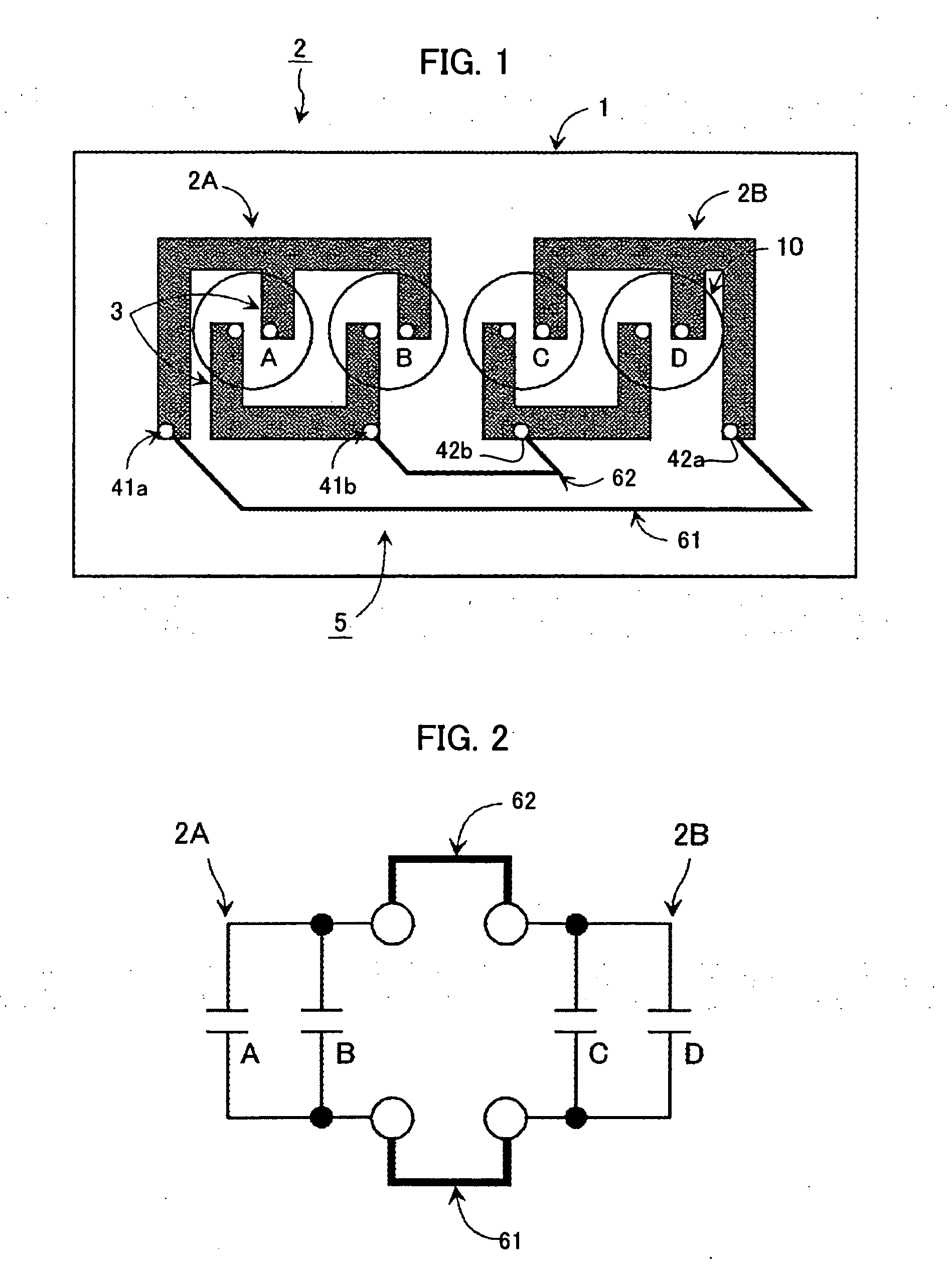
1. Field of the Invention The present invention relates to a printed circuit board structure, and more particularly to a printed circuit board structure suitable for use in an inverter for driving an electric motor. 2. Description of Related Art An inverter device is widely used for driving an induction motor since it drives a general-purpose induction motor efficiently at variable speed. The inverter devices have difference specifications in connection of external cables, rated voltages and allowable input voltages for different usages, and it has been a general practice to modify the whole. constitution or components of the inverter to cope with a specific usage. For instance, a plurality of capacitors are used in parallel for a low-voltage power source specification, and a combination of a serial connection and a parallel connection of capacitors are used for a high voltage power source specification in view of allowable input voltages of the capacitors. It has been proposed to prepare plural kinds of printed circuit boards which have circuit elements of different rated voltages on the same conductive patterns and select one kind of these printed circuit boards to be mounted so that only a power circuit board is changeable with using the same control circuit board, in order to avoid a rise of cost in modification of the whole constitution or components of the inverter device for coping with difference specifications in connection of external cables, rated voltages and allowable input voltages, as seen in JP 06-303779A, for example, paragraphs-[0009] thereof. In this conventional arrangement, the printed circuit boards may cope with different voltage specifications by preparing the plural kinds of printed circuit boards having different circuit elements with the same conductive pattern, but this arrangement has a limitation in application to various specifications since the circuit parts have limited allowable input voltages. The present invention can cope with different input voltage levels by changing connection of circuit parts from a parallel connection to a combination of serial and parallel connections even if an input voltage exceeds an allowable voltage of the circuit parts. Further, the number of kinds of printed circuit boards for constituting an inverter device are reduced by using the same conductive patters as common elements for forming a capacitor circuit. A printed circuit board structure of the present invention comprises: a plurality of conductive patterns each including at least one pair of electrodes to form a capacitor, and terminals electrically conducted with the electrodes; and selective connection means for selectively connecting the terminals of the conductive patterns so that a capacitor circuit having predetermined capacitance is formed. The selective connection means may comprise one or more short bars formed on a circuit board on which the plurality of conductive patterns are formed. Alternatively, the plurality of conductive patterns may be formed on respective circuit boards, and the selective connection means may comprise a conductive pattern formed on a circuit board separately form the respective circuit boards for the plurality of conductive patterns. The plurality of conductive patterns may be constituted by a combination of the same electrode arrangements and/or different electrode arrangements. Any ones of the electrodes, the short bars and the conductive patterns may be formed by artwork. The capacitor circuit may be used for smoothing an input voltage of an inverter for driving an electric motor. In this case, the terminals of the conductive patterns are selectively connected by the selective connection means so that the inverter device has an allowable input voltage appropriate for the input voltage. According to the above arrangement of the present invention, the same conductive patters are used as common elements for forming capacitor circuits having different allowable input voltages, and thus the number of kinds of printed circuit boards for constituting an inverter device are reduced. A first embodiment of the present invention will be described referring to The two conductive patterns 2A and 2B formed on the circuit board 1 have substantially the same patterns and each of the conductive patterns 2A and 2B has two pairs of electrodes 3 arranged in confronting relation. A printed circuit board 2′ shown in The two pairs of electrodes 3 provided in the conductive pattern 2A constitute capacitors A and B in regions 10 indicated by circles in The conductive pattern 2A has terminals 41 The printed circuit board 2 shown in Thus, a parallel circuit of the capacitors A and B and a parallel circuit of the capacitors C and D are connected in parallel by the short bars 61 and 62, so that a capacitor circuit comprising the capacitors A, B, C and D in parallel as a whole is formed on the circuit board 1, an equivalent circuit of which is shown in The printed circuit board 2′ shown in It is notable that any arbitrary number of conductive patterns may be provided on the circuit board 1, although two conductive patters 2A and 2B are provided in the circuit board 1 in the above embodiment. A second embodiment of the present invention is shown in As shown in The two conductive patterns 2C and 2D formed on the circuit board 1 have the same patterns and each of the conductive patterns 2C and 2D has one pair of electrodes 3 arranged in confronting relation. A printed circuit board shown in The pair of electrodes 3 provided in the conductive pattern 2C constitutes a capacitor A in a region 10 indicated by a circle in The conductive pattern 2C has terminals 41 The printed circuit board shown in Thus, a capacitor circuit comprising the capacitors A and B connected in parallel is formed on the circuit board 1. The printed circuit board shown in A third embodiment of the present invention are shown in In the third embodiment, at least one conductive pattern is formed on each of a plurality of circuit boards 1 One or more short bars are used as the selective connector for selectively connecting the conductive patterns in the first and second embodiments. In this third embodiment, a conductive pattern formed on a circuit board 1 In a printed circuit board structure shown in The pair of electrode 3 provided in the conductive pattern 2C forms a capacitor A in a region 10 indicated by a circle and the pair of electrode 3 provided in the conductive pattern 2D forms a capacitor B in a region 10 indicated by a circle. Thus, each of the conductive pattern 2C and the conductive pattern 2D constitutes a fundamental unit having one capacitor. The conductive pattern 2C has terminals A1 and A2, and the conductive pattern 2D has terminals B1 and B2. Terminals A1′, A2′ and B1′, B2′ are provided on the circuit board 1 In the arrangement shown in In the arrangement shown in The connection among the printed circuit boards 1 With the arrangement shown in In the above examples shown in An inverter device may be constituted by using the above printed circuit board structure as a capacitor in an existing circuitry arrangement. When an input voltage of the inverter device or characteristics of external circuitry is changed, an appropriate capacitance of the capacitor circuit is obtained by using a different selective connector. Since different capacitances are obtained by using the same printed circuit boards and replacing the conductive pattern or short bars as the selective connector, the printed circuit boards can be used as common elements of the capacitor circuit. The above-described embodiments are directed to variation of the allowable input voltage of the capacitor circuitry. The present invention may be applied to a circuitry having elements other than capacitor on the circuit board so that a desired allowable input voltage of the circuitry is obtained by a combination of the elements in series and parallel. The present invention is not limited to an application on an inverter device but is applicable to a device requiring a change of allowable input voltage with printed circuit boards using as common elements. A printed circuit board structure for a motor driving device in which the number of kinds of printed circuit boards for constituting inverter devices having different allowable input voltages are reduced. This printed circuit board structure comprises a plurality of conductive patterns and a selective connector. Each of the conductive patterns includes at least one pair of electrodes arranged in confronting relation to form a capacitor, and terminals electrically conducted with the electrodes. The selective connector selectively connects the terminals of the conductive patterns so that a capacitor circuit having predetermined capacitance is formed. 1. A printed circuit board structure comprising:
a plurality of conductive patterns each including at least one pair of electrodes to form a. capacitor, and terminals electrically conducted with the electrodes; and selective connection means for selectively connecting the terminals of said conductive patterns so that a capacitor circuit having predetermined capacitance is formed. 2. A printed circuit board structure according to 3. A printed circuit board structure according to 4. A printed circuit board structure according to 5. A printed circuit board structure according to 6. A printed circuit board structure according to BACKGROUND OF THE INVENTION
SUMMARY OF THE INVENTION
BRIEF DESCRIPTION OF THE DRAWINGS
DETAILED DESCRIPTION