ACCUMULATOR-TYPE FRACTIONAL N-PLL SYNTHESIZER AND CONTROL METHOD THEREOF
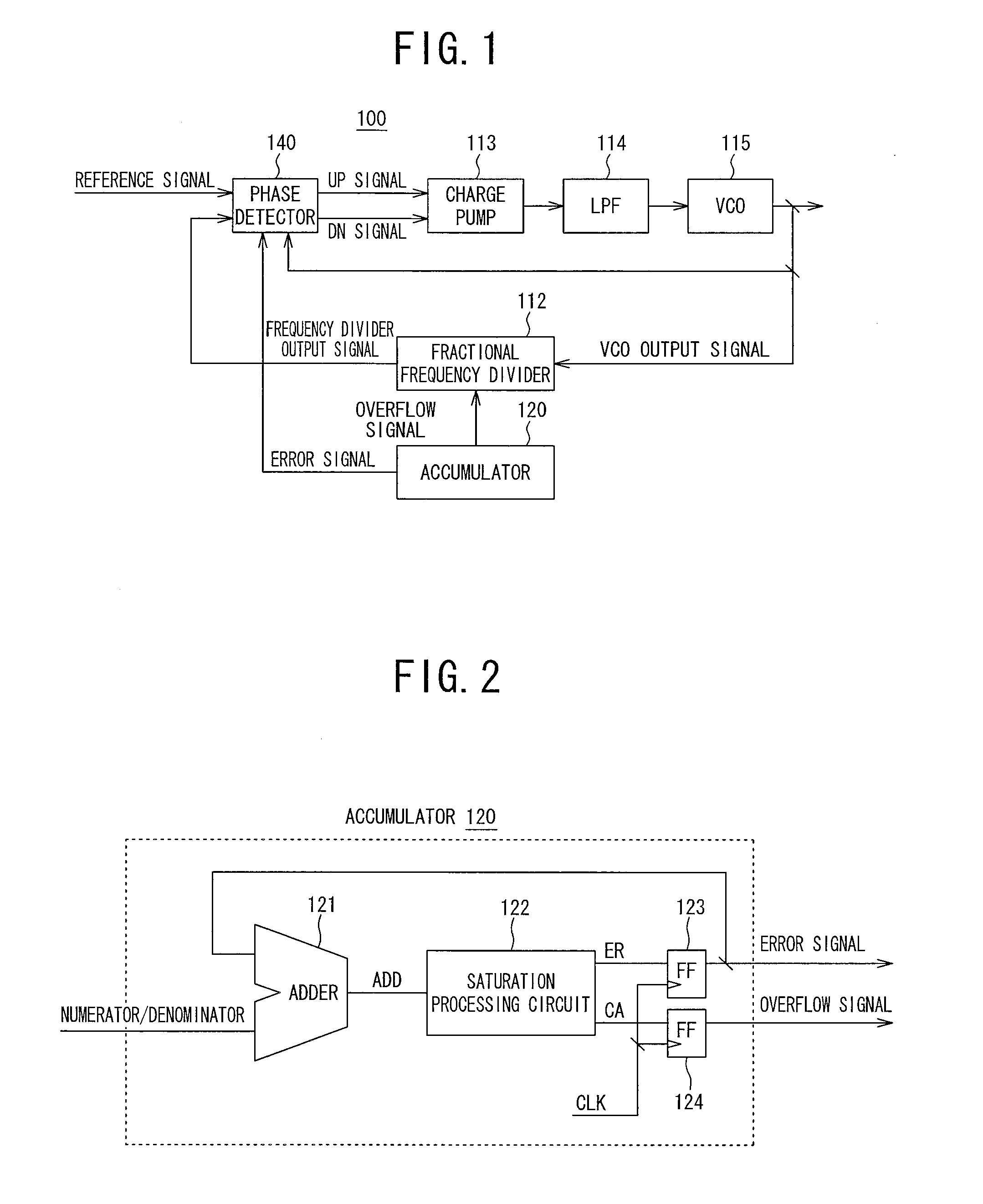
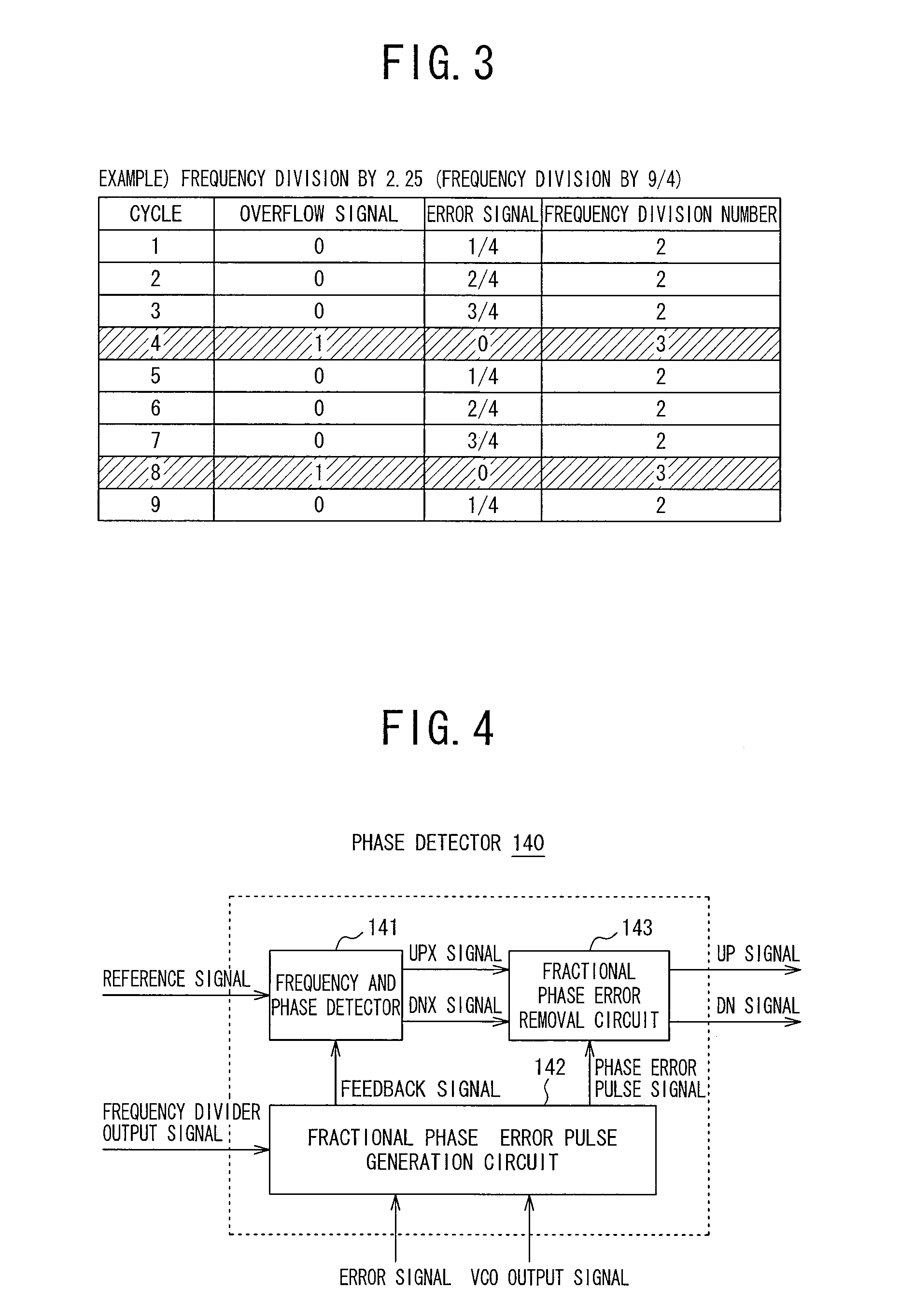
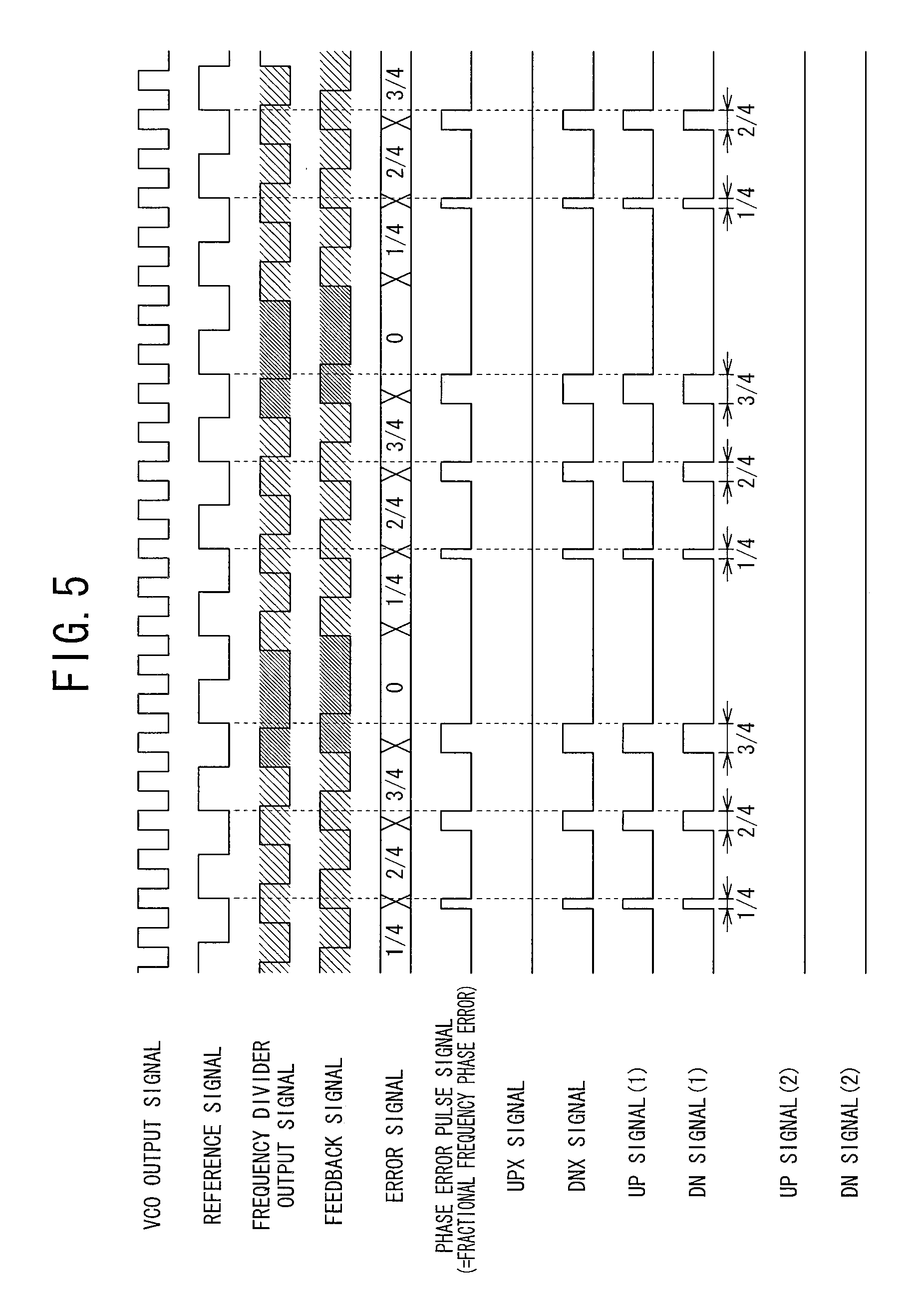
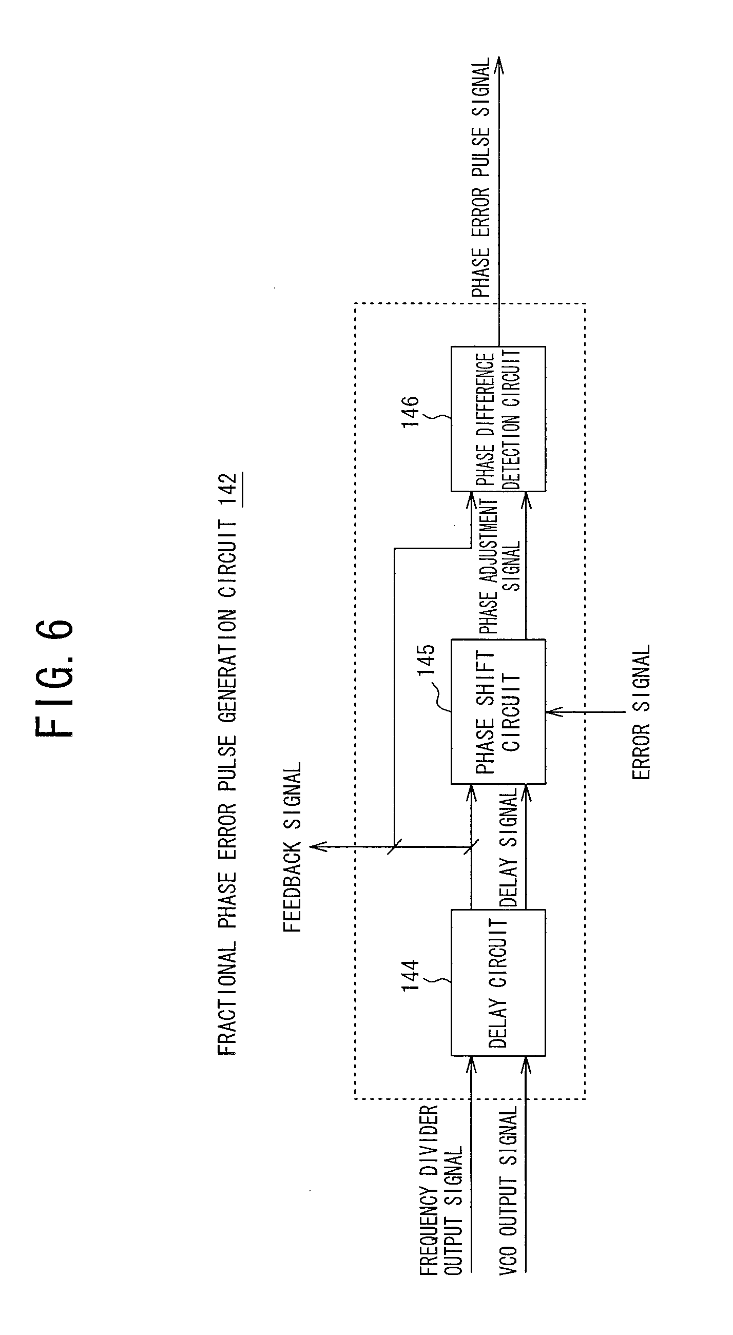
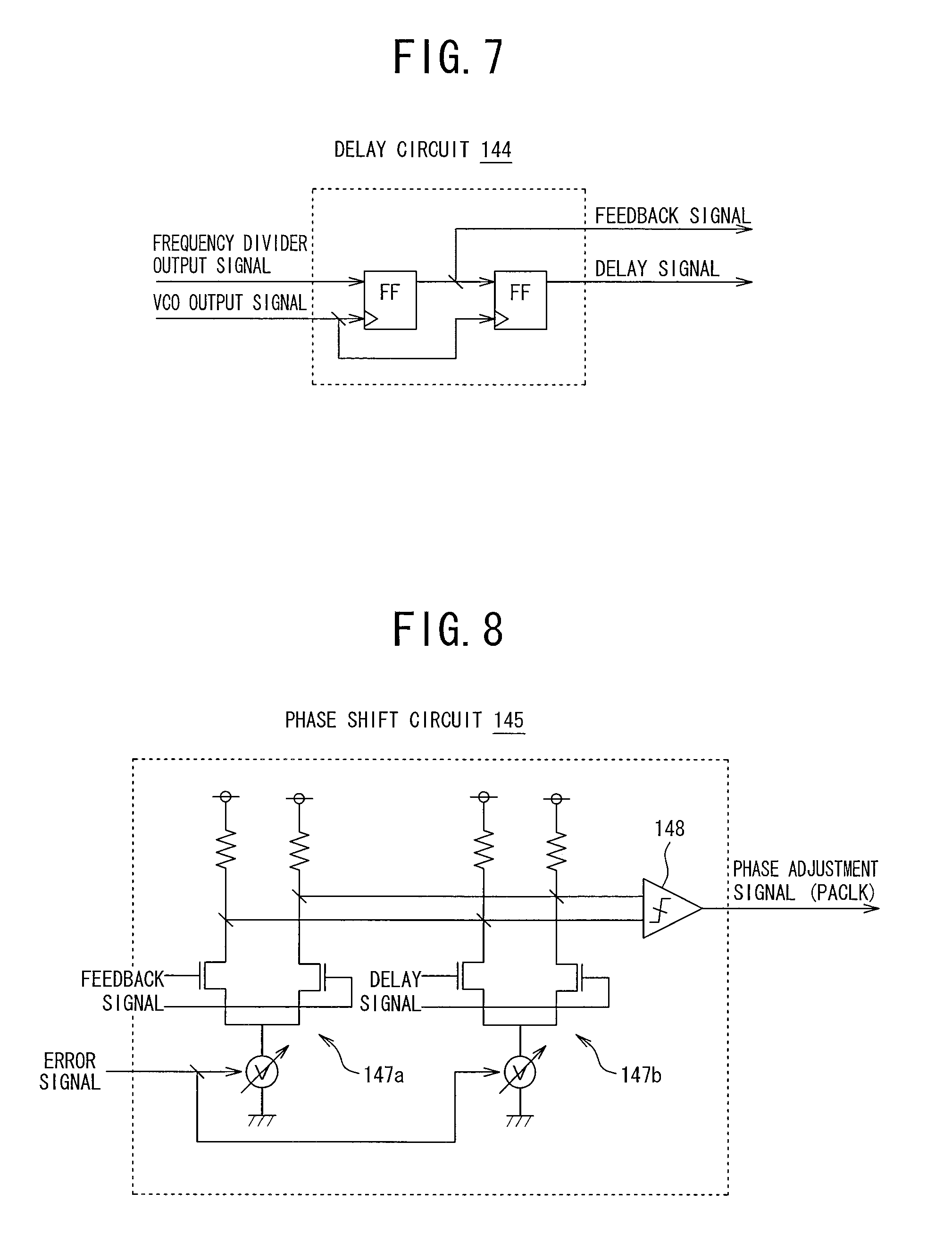
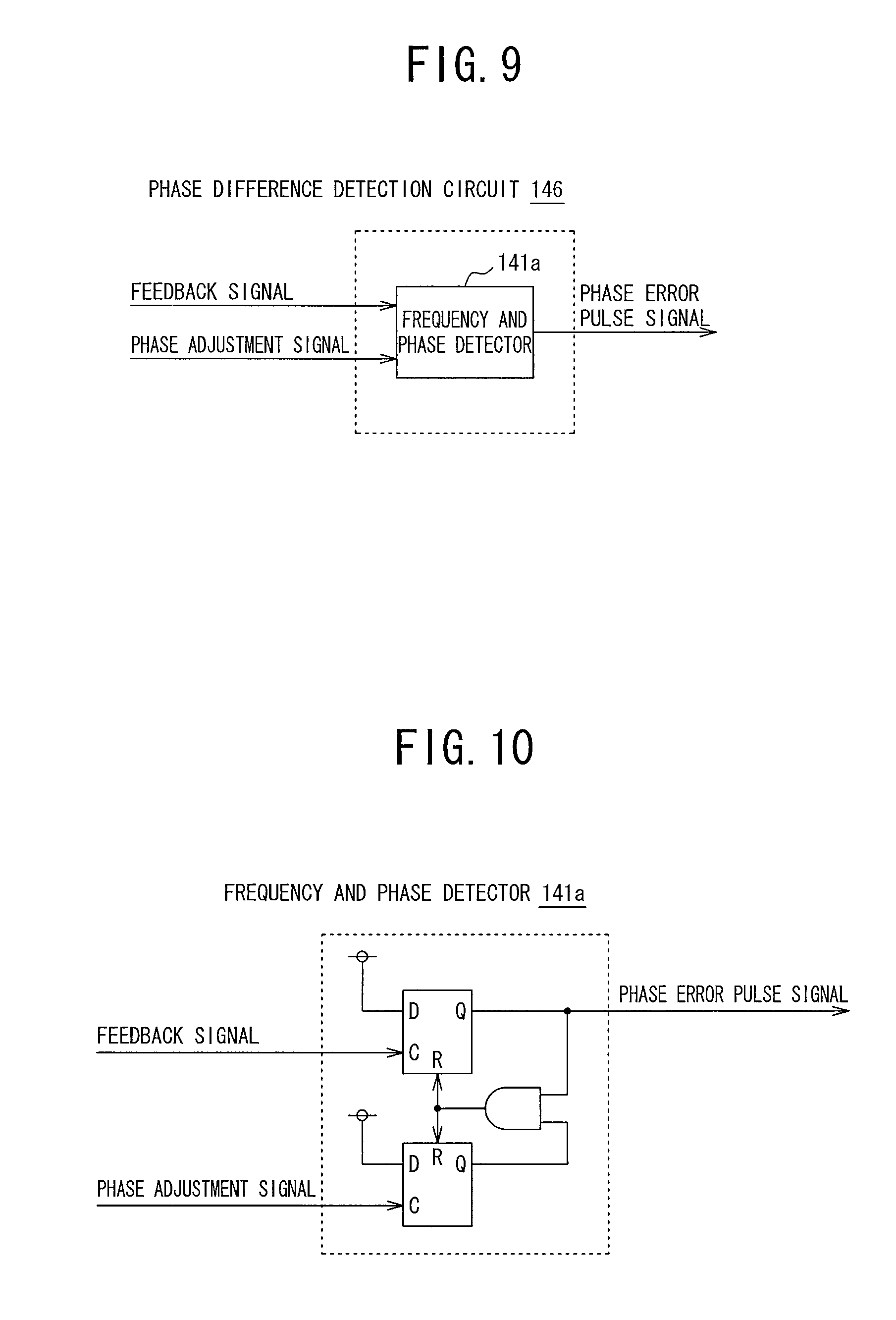
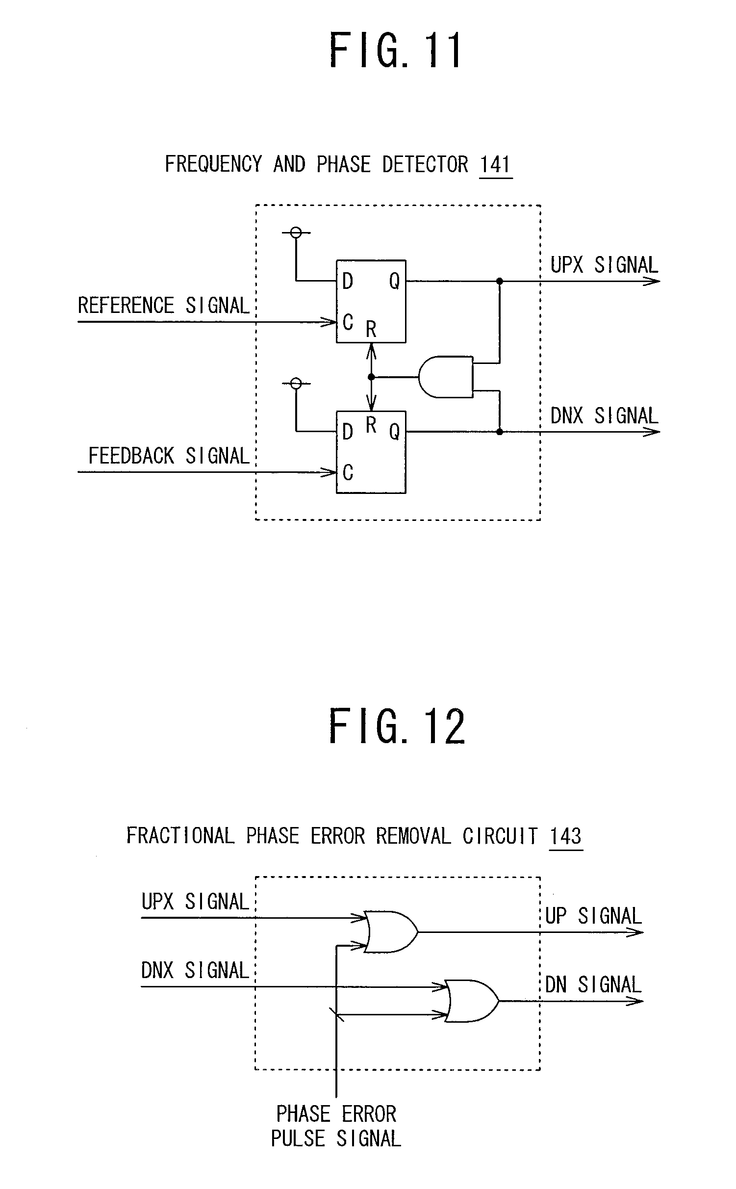
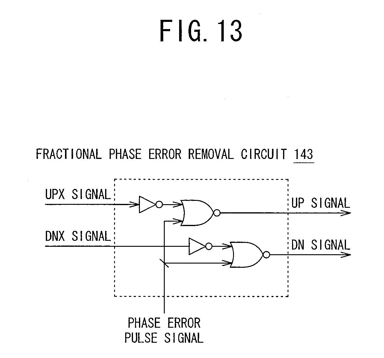
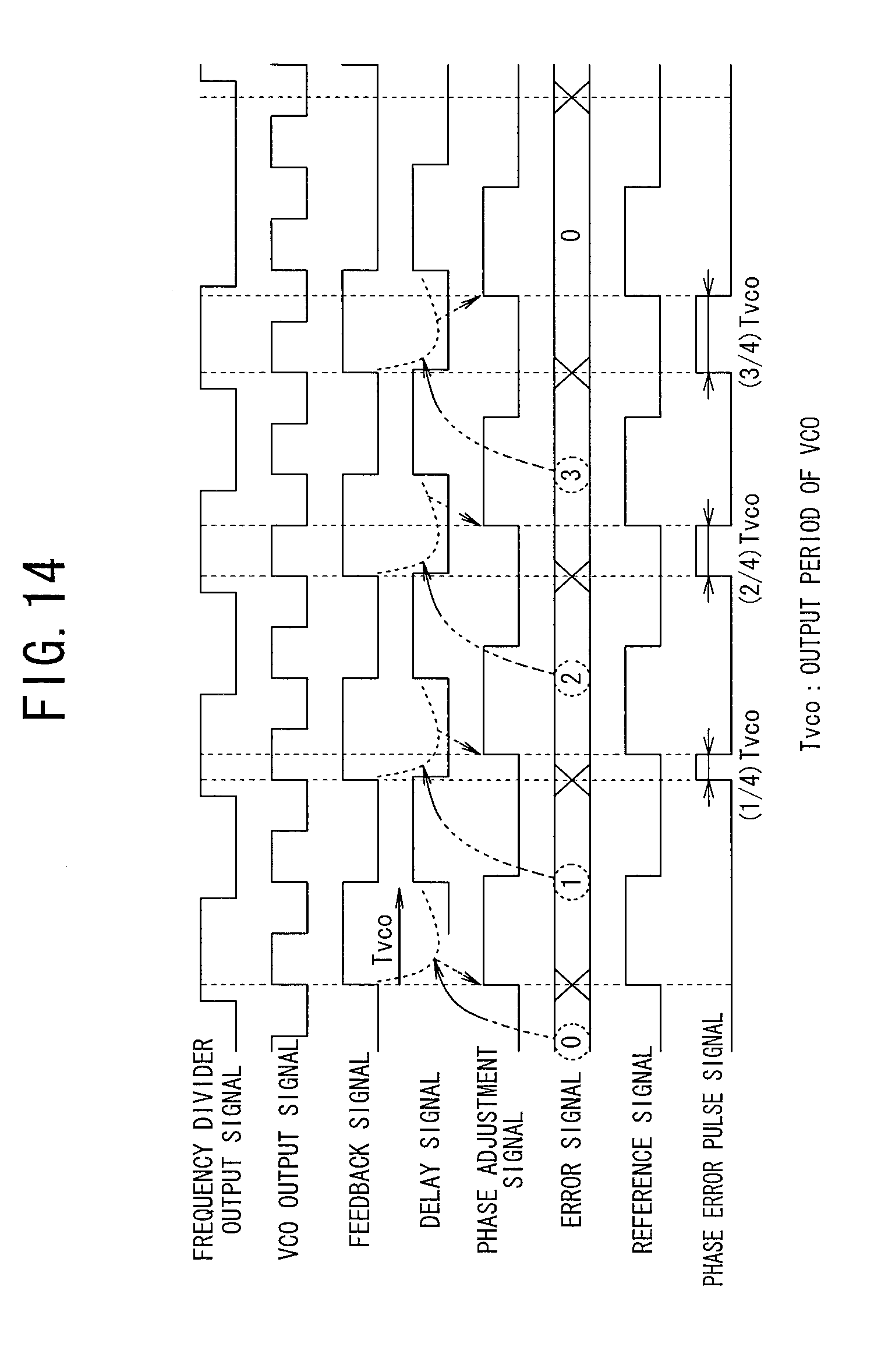
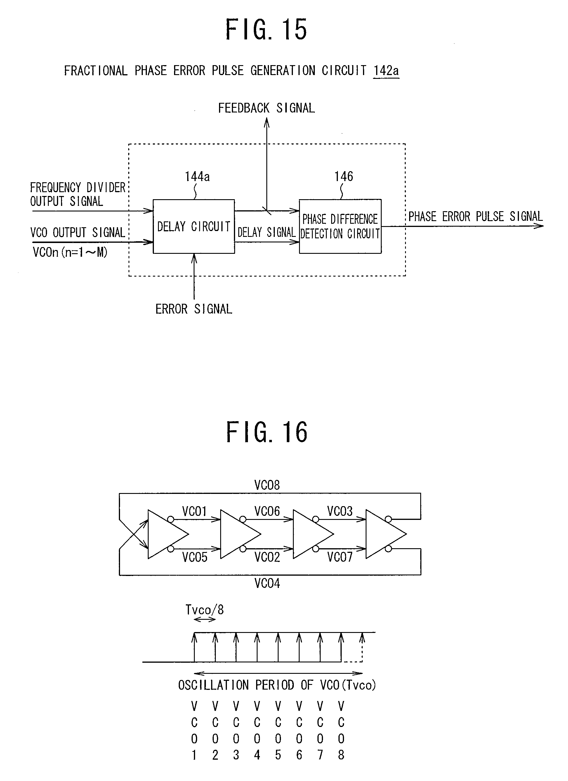
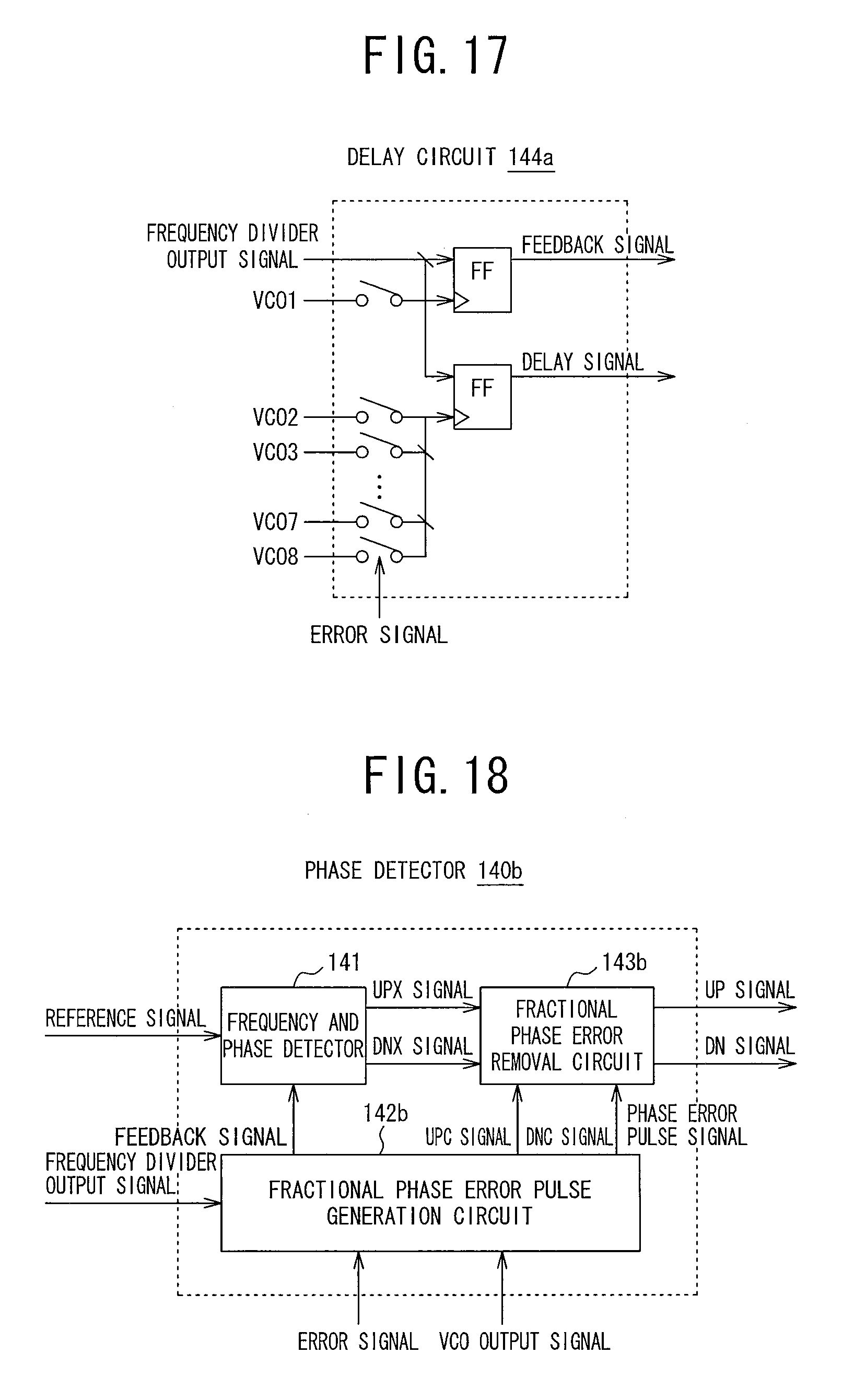
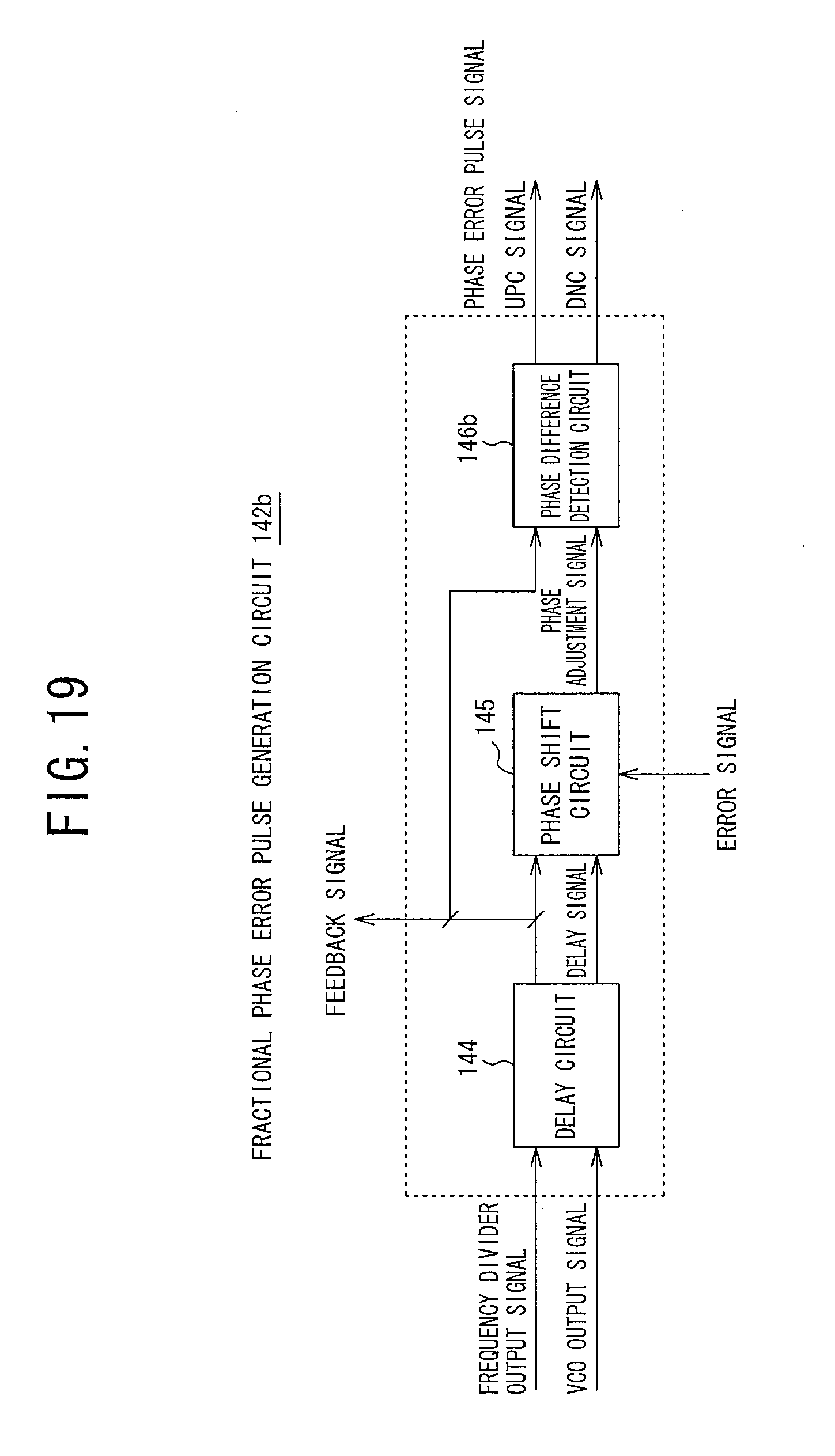
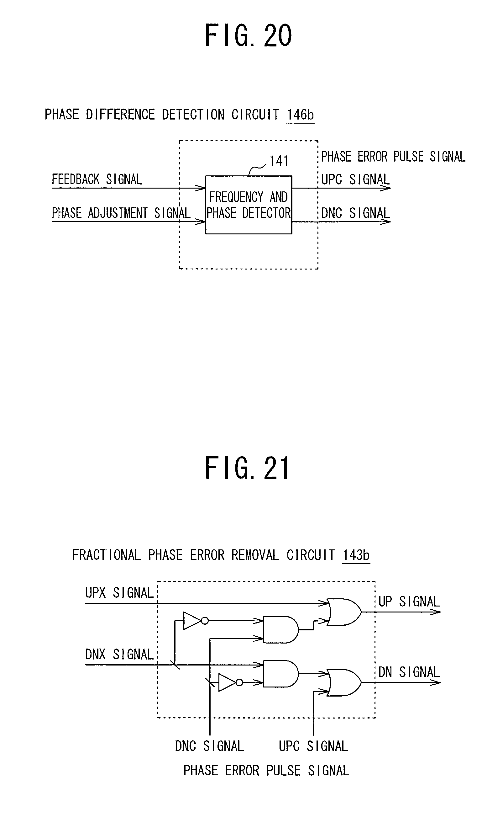
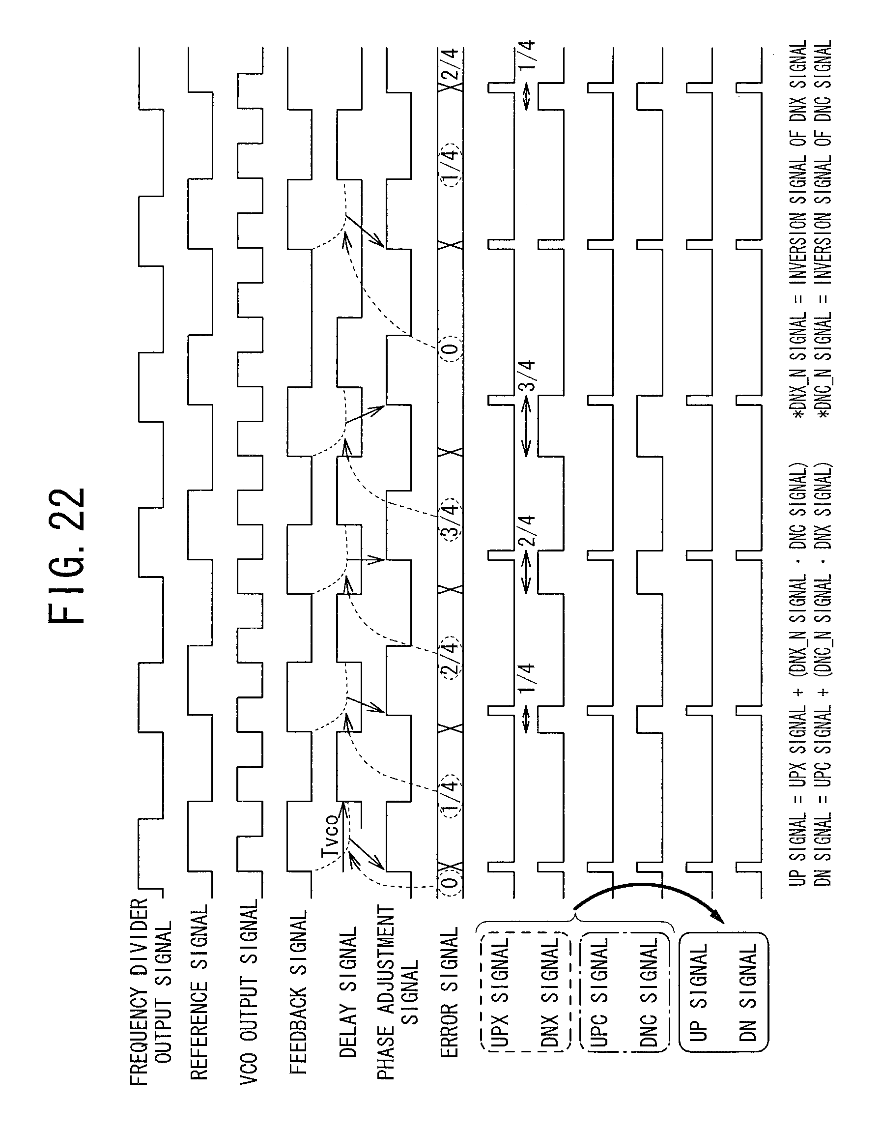
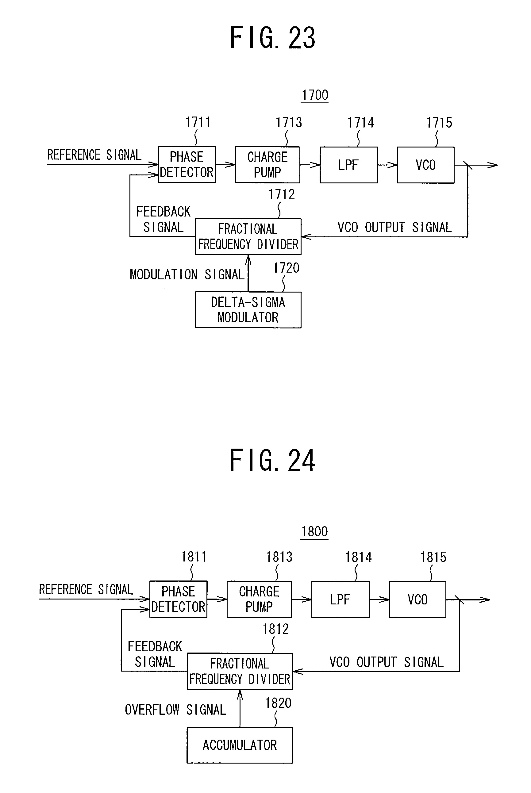
The present invention relates to fractional N-PLL synthesizers, more particularly to an accumulator-type fractional N-PLL synthesizer for controlling a fractional frequency division number using an accumulator and a control method thereof. A fractional N-PLL synthesizer is a PLL characterized in that a feedback frequency division number for frequency-dividing an output of a voltage-controlled oscillator (hereafter, VCO) is a fractional frequency division number. In The phase detector 1711 detects the phase difference between the reference signal and the feedback signal output from the fractional frequency divider 1712, and outputs the detected phase difference to the charge pump 1713. The charge pump 1713 outputs an amount of charge corresponding to the phase difference, to the LPF 1714. The VCO 1715 changes an output frequency according to an output of the LPF 1714. The fractional frequency divider 1712 divides an output signal of the VCO 1715 by a predetermined division ratio, and outputs the divided signal to the phase detector 1711. The delta-sigma modulator 1720 temporally switches the frequency division number in the fractional frequency divider 1712 between frequency division by N and frequency division (N+1), according to a set value of a numerator and a denominator of a feedback frequency division number. For example, let Fref be a frequency of the reference signal, and N+NUM/DEN (where N, NUM, and DEN are each an integer) be the feedback frequency division number. An oscillation frequency FVCO of the output signal of the VCO 1715 is expressed as Transforming Expression (1) yields By switching the frequency division number between frequency division by N and frequency division by (N+1) in a time proportion according to Expression (2), the fractional frequency divider 1712 realizes a fractional frequency division number. Moreover, the feedback frequency division number is aperiodically switched through the use of delta-sigma modulation. This produces an advantage that fractional spurious which is inherent spurious corresponding to switching periodicity is unlikely to occur. However, in the system described above with reference to Here, the PLL has a function as a low-pass filter, but, when viewed from the LPF and the VCO which are elements of the PLL, functions as a high-pass filter (hereafter, HPF). Accordingly, low-frequency noise component generated from the elements such as the LPF and the VCO is removed by the function of the PLL as a low-pass filter. Low-frequency noise component can be removed more efficiently when the cutoff frequency of the low-pass filter as the function of the PLL is higher. Due to the above-mentioned circumstances, the delta-sigma-type fractional N-PLL synthesizer cannot sufficiently remove low-frequency noise generated from the LPF and the VCO constituting the PLL, resulting in that a problem of degradation in output signal performance (jitter) of fractional N-PLL synthesizers still remains. In The accumulator-type fractional N-PLL employs a system of realizing a fractional frequency division number by periodically switching the frequency division number of the fractional frequency divider 1812 according to an output of the accumulator 1820. In this system, there is no need to remove high-frequency noise because the delta-sigma modulator as in the system in However, the conventional accumulator-type fractional N-PLL synthesizer described with reference to The present invention has been made in view of the above-mentioned circumstances, and has an object of providing an accumulator-type fractional N-PLL synthesizer with less fractional spurious, and a control method thereof. To solve the problems stated above, the following techniques are proposed. (1) According to an aspect of the present invention, there is provided an accumulator-type fractional N-PLL synthesizer including: a VCO; a fractional frequency divider disposed in a feedback path of an output signal of the VCO, for generating a frequency divider output signal of a fractional frequency division number; an accumulator for supplying an overflow signal for periodically switching the frequency division number of the fractional frequency division number, to the fractional frequency divider; and a phase detector for detecting a phase difference between the frequency divider output signal and a predetermined reference signal to generate a control input signal to the VCO based on the detected phase difference, wherein the accumulator generates an error signal having fractional phase error information, and wherein the phase detector corrects the phase difference between the frequency divider output signal and the reference signal, using the error signal. (2) The phase detector may generate the phase difference as a UP signal and a DN signal, and supply the generated UP signal and DN signal to a charge pump for generating the control input signal. (3) The phase detector may include: a fractional phase error pulse generation circuit for generating a phase error pulse signal having a pulse width proportional to a fractional phase error and generating a feedback signal, based on the frequency divider output signal and the error signal; a frequency and phase detector for generating a frequency and phase detection output signal having a pulse width proportional to a difference in frequency and phase between the reference signal and the feedback signal; and a fractional phase error removal circuit for generating the UP signal and the DN signal with the fractional phase error included in the frequency and phase detection output signal being reduced based on the phase error pulse signal. (4) The fractional phase error removal circuit may include a logical circuit for taking a logical sum of the frequency and phase detection output signal and the phase error pulse signal. (5) The fractional phase error removal circuit may include a logical circuit including a NOT circuit and a NOR circuit for removing the fractional phase error included in the frequency and phase detection output signal using the phase error pulse signal. (6) The fractional phase error removal circuit may remove the fractional phase error occurring between two output signals which are a UPX signal and a DNX signal included in the frequency and phase detection output signal, by performing logical operations of using the phase error pulse signal including a UPC signal and a DNC signal, where the DNX_N signal is an inversion signal of the DNX signal, and the DNC_N signal is an inversion signal of the DNC signal. (7) The fractional phase error pulse generation circuit may include: a delay circuit for generating the feedback signal and a delay signal having a predetermined time delay with respect to the feedback signal, based on the frequency divider output signal; a phase shift circuit for generating a phase adjustment signal based on the feedback signal, the delay signal, and the error signal; and a phase difference detection circuit for generating the phase error pulse signal having a pulse width proportional to a phase difference between the feedback signal and the phase adjustment signal. (8) The fractional phase error pulse generation circuit may include: a delay circuit for generating the feedback signal and a delay signal that has a predetermined time delay with respect to the feedback signal, based on the frequency divider output signal; a phase shift circuit for generating a phase adjustment signal based on the feedback signal, the delay signal, and the error signal; and a phase difference detection circuit for generating a UPC signal and a DNC signal as the phase error pulse signal having a pulse width proportional to a phase difference between the feedback signal and the phase adjustment signal. (9) The delay circuit may generate the feedback signal and the delay signal to be delayed by a period of the output signal with respect to the feedback signal, based on an input signal to the delay circuit. (10) The phase shift circuit may be supplied with the feedback signal and the delay signal, and generate the phase adjustment signal by performing phase shift on the feedback signal based on the error signal. (11) The fractional phase error pulse generation circuit may include: a delay circuit for generating a delay signal delayed by an integer multiple of 1/M of an output period of the VCO with respect to the feedback signal where M is a natural number, based on the error signal; and a phase difference detection circuit for generating the phase error pulse signal having a pulse width proportional to a phase difference between the feedback signal and the delay signal. (12) The delay circuit may select one signal out of the frequency divider output signal and a plurality of signals each delayed by an integer multiple of 1/M of an output period of the VCO where M is a natural number, based on the error signal. (13) The error signal may be a signal that gradually changes in each period of the overflow signal. (14) According to another aspect of the present invention, there is provided an accumulator-type fractional N-PLL synthesizer including: an accumulator; and a phase detector for generating a UP signal and a DN signal with a fractional phase error which occurs between a reference signal and a frequency divider output signal being reduced based on an error signal from the accumulator. (15) According to still another aspect of the present invention, there is provided a control method of an accumulator-type fractional N-PLL synthesizer, for controlling a phase detector to generate a UP signal and a DN signal with a fractional phase error which occurs between a reference signal and a frequency divider output signal being reduced based on an error signal from an accumulator. According to the present invention, it is possible to realize an accumulator-type fractional N-PLL synthesizer with less fractional spurious. Embodiments of the present invention will now be described in detail to demonstrate the present invention. In The accumulator-type fractional N-PLL synthesizer 100 is the same as the accumulator-type fractional N-PLL synthesizer 1800 described above with reference to The accumulator-type fractional N-PLL synthesizer 100 in this embodiment has a feature that an error signal from the accumulator 120 and a VCO output signal from the VCO 115 are input to the phase detector 140, as will be described in detail later. Next, a description will be give of the accumulator 120, the fractional frequency divider 112, and the phase detector 140 in the accumulator-type fractional N-PLL synthesizer 100, with reference to drawings. In The output ER of the saturation processing circuit 122 is input to a flip-flop (FF) 123, and the other output CA of the saturation processing circuit 122 is input to a flip-flop (FF) 124. A clock signal CLK is input to each of the flip-flops 123 and 124. The flip-flop 123 outputs the output ER of the saturation processing circuit 122 as an error signal, in synchronization with the clock signal CLK. Likewise, the flip-flop 124 outputs the other output CA of the saturation processing circuit 123 as an overflow signal, in synchronization with the clock signal CLK. 00010001 . . . . This switches the frequency division number of the fractional frequency divider as 22232223 . . . , thus generating four clock edges while counting nine input clock edges. The fractional frequency division by 9/4 is achieved in this way. Meanwhile, pre-overflow accumulation information is output from the accumulator 120 as 1/4, 2/4, 3/4, 0, 1/4, 2/4, 3/4, 0 . . . , as the error signal. The value of the error signal mentioned above represents the period of the output signal of the VCO 115, as a unit value. The above-mentioned error signal is not a difference (deviation) between the result of the accumulation process in the accumulator 120 and some kind of reference value, but a phase adjustment signal whose value is used for performing phase adjustment on a signal to be adjusted. This value, however, corresponds to a deviation between the signal to be phase-adjusted and the reference signal that serves as the reference, as will be described later. As can be understood from above description, the accumulator 120 is configured to: generate the error signal for phase adjustment that cyclically changes in the output period of the VCO 115 while gradually changing in its accumulation value at each time interval obtained by dividing the period of the output signal of the VCO 115 by a predetermined natural number, and supply the error signal to the phase detector 140; and also generate the overflow signal described with reference to The phase detector 140 in The phase detector 140 is configured to correct and detect the phase difference between the frequency divider output signal supplied from the fractional frequency divider 112 as a feedback signal and a predetermined reference signal by reflecting the error signal supplied from the accumulator 120 and the output signal of the VCO 115 so as to reduce a fractional phase error. The structure and operation of the phase detector 140 will be described in more detail later with reference to drawings. The fractional phase error pulse generation circuit 142 generates the feedback signal to the frequency and phase detector 141, and a phase error pulse signal that is proportional to the fractional phase error and that is supplied to the fractional phase error removal circuit 143, based on the frequency divider output signal from the fractional frequency divider 112, the VCO output signal from the VCO 115, and the error signal from the accumulator 120. The frequency and phase detector 141 compares frequencies and phases between a predetermined reference signal and the feedback signal from the fractional phase error pulse generation circuit 142, and generates a UPX signal and a DNX signal corresponding to differences as a result of comparison. The fractional phase error is included between the UPX signal and the DNX signal. The fractional phase error removal circuit 143 controls pulse widths of the UPX signal and the DNX signal including the fractional phase error from the frequency and phase detector 141 based on the phase error pulse signal from the fractional phase error pulse generation circuit 142, thereby obtaining a UP signal and a DN signal with the reduced fractional phase error. The fractional phase error removal circuit 143 then supplies the obtained UP signal and DN signal to the charge pump 113 ( The phase detector 140 in the accumulator-type fractional N-PLL synthesizer 100 in As can be understood from As can be easily understood by comparing The fractional phase error removal circuit 143 can use a method of outputting logical addition results of the phase error pulse signal to both the UPX signal and the DNX signal to the charge pump 113 respectively as a UP signal and a DN signal, and a method of outputting logical subtraction results of the phase error pulse signal from both the UPX signal and the DNX signal to the charge pump 113 respectively as the UP signal and the DN signal. In the former method of taking the logical sum, the UP signal and the DN signal output to the charge pump 113 have the same pulse width with respect to the fractional phase error in a state where the fractional N-PLL synthesizer 100 is locked (see UP signal (1) and DN signal (1) in In the latter method of taking the logical difference, the fractional phase error is not included in any of the UP signal and the DN signal output to the charge pump 113 in a state where the fractional N-PLL synthesizer 100 is locked (see UP signal (2) and DN signal (2) in In the above-mentioned manner, the problem of the fractional spurious in the conventional accumulator-type fractional N-PLL described above with reference to When compared with another technique in which the periodic charge output from the charge pump causing the fractional spurious is canceled out by the output of another charge pump newly provided, the accumulator-type fractional N-PLL synthesizer in this embodiment does not need another charge pump circuit, and so does not have any problem of consistency in the current amount or operation timing between two charge pumps. Hence, the accumulator-type fractional N-PLL synthesizer in this embodiment produces a more prominent advantageous effect of reducing the fractional spurious. Moreover, when compared with the delta-sigma-type fractional N-PLL synthesizer described above with reference to Furthermore, the typical delta-sigma-type fractional N-PLL synthesizer has a problem that the denominator in fractional frequency division needs to be a fixed value and an arbitrary frequency cannot be generated without causing a frequency error. This embodiment, on the other hand, is also characterized by employing the accumulator-type fractional N-PLL synthesizer system, and therefore exhibits an excellent feature that an arbitrary frequency can be generated without causing a frequency error. The fractional phase error pulse generation circuit 142 in Though a dual-modulus frequency divider for performing frequency division by N or frequency division by (N+1) is used as an example of the above-mentioned fractional frequency divider 112, the present invention is not limited to this example, and may employ various specifications such as frequency division by N and frequency division by (N+2). In a case of employing the specifications of frequency division by N and frequency division by (N+2), it is more desirable that the phase difference between the delay signal and the reference signal be equal to twice the oscillation period of the VCO 115. The phase shift circuit 145 provided in the next stage of the above-mentioned delay circuit 144 in the fractional phase error pulse generation circuit 142 in The phase difference detection circuit 146 provided in the next stage of the above-mentioned delay circuit 144 and phase shift circuit 145 in the fractional phase error pulse generation circuit 142 in The delay circuit 144 in The phase shift circuit 145 in The frequency and phase detector 141 The frequency and phase detector 141 in The fractional phase error pulse generation circuit 142 will be further described below, with reference to The delay circuit 144 in the fractional phase error pulse generation circuit 142 generates the feedback signal to the frequency and phase detector 141 and the delay signal delayed by the oscillation period of the VCO 115 with respect to the feedback signal, based on the frequency divider output signal and the VCO output signal which are both input to the delay circuit 144. The phase shift circuit 145 in the fractional phase error pulse generation circuit 142 generates the phase adjustment signal as the output of the phase shift circuit 145, by phase shifting between the rising edges of the feedback signal and the delay signal which are both input to the phase shift circuit 145. For example, in a case where the error signal from the accumulator 120 is 1/4 of a unit with one period of the output signal from the VCO 115 being as the unit, the rising edge of the phase adjustment signal is situated at a position of 1/4 between the rising edges of the feedback signal and the delay signal. In a case where the error signal is 2/4 thereof in the next step, the rising edge of the phase adjustment signal is situated at a center position between the rising edges of the feedback signal and the delay signal. The phase difference detection circuit 146 generates the phase error pulse signal whose pulse width corresponds to the phase difference between the rising edges of the feedback signal and the phase adjustment signal which are both input to the phase difference detection circuit 146. As can be understood from the above description, the phase error pulse signal corresponding to the fractional phase error which occurs between the UPX signal and the DNX signal output from the frequency and phase detector 141 can be generated by the fractional phase error pulse generation circuit 142 illustrated in A fractional phase error pulse generation circuit 142 The delay circuit 144 The delay circuit 144 As can be understood from above description, in the case where the fractional phase error is an integer multiple of 1/8 of the output period of the VCO 115, the delay signal delayed by the fractional phase error with respect to the feedback signal can be obtained by controlling the switches connected to VCOn (n=2 to 8) according to the error signal from the accumulator 120. Following this, the phase error pulse signal equal to the fractional phase error can be generated by the phase difference detection circuit 146 generating the phase error pulse signal whose pulse width corresponds to the phase difference between the rising edges of the feedback signal and the delay signal which are both input to the phase difference detection circuit 146. Thus, this embodiment has a characteristic feature that the phase shift circuit 145 as illustrated in The above description has been given to the case where the fractional phase error is an integer multiple of 1/8 of the output period of the VCO 115. Even in a case where the fractional phase error is not an integer multiple of 1/8 of the output period of the VCO 115, however, the delay amount may be selected so that both values are approximate to each other. In such a case, it is impossible to completely eliminate the fractional spurious, but a practically sufficient fractional spurious reduction effect can still be achieved by increasing the number of stages of the VCO 115 to set a sufficiently fine step size of the delay amount. A phase detector 140 The phase detector 140 The fractional phase error pulse generation circuit 142 The frequency and phase detector 141 compares frequencies and phases between a predetermined reference signal and the feedback signal from the fractional phase error pulse generation circuit 142 The fractional phase error removal circuit 143 The fractional phase error pulse generation circuit 142 Note that the structure of the fractional phase error removal circuit 143 is not limited to those illustrated in The phase detector 140 As can be understood from Accordingly, the fractional phase error pulse generation circuit 142 is then performed to remove the fractional phase error occurring between the UPX signal and the DNX signal using the UPC signal and the DNC signal, and output the UP signal and the DN signal corresponding to the phase difference between the reference signal and the feedback signal (phase adjustment signal), where the DNX_N signal=an inversion signal of the DNX signal and the DNC_N signal=an inversion signal of the DNC signal. As can be understood from above description, the technique described with reference to The scope of the present invention is not limited to the illustrative embodiments described and depicted herein, and includes all embodiments which produce equivalent advantageous effects as intended by the present invention. Moreover, the scope of the present invention is not limited to the combination of the features of the invention defined by claim 1, and can be defined by any desired combination of specific features out of all disclosed features. There are provided an accumulator-type fractional N-PLL synthesizer for suppressing the fractional spurious caused by periodically switching a frequency division number of a fractional frequency divider, and a control method thereof. In an accumulator-type fractional N-PLL synthesizer (100), a pulse signal proportional to a fractional phase error occurring between a reference signal and an output signal of a fractional divider (112) for feeding back an output of a VCO (115) of an output stage to a preceding stage is generated using an error signal from an accumulator (120). Through the use of the pulse signal, pulse widths of a UP signal and a DN signal output from a phase detector (140) are controlled so as to reduce a fractional phase error occurring between the UP signal and the DN signal. Thus, the fractional spurious caused by periodically switching the frequency division number of the fractional divider (112) is suppressed. 1. An accumulator-type fractional N-PLL synthesizer comprising:
a VCO; a fractional frequency divider, disposed in a feedback path of an output signal of the VCO, for generating a frequency divider output signal of a fractional frequency division number; an accumulator for supplying an overflow signal for periodically switching a frequency division number of the fractional frequency division number, to the fractional frequency divider; and a phase detector for detecting a phase difference between the frequency divider output signal and a predetermined reference signal to generate a control input signal to the VCO based on the detected phase difference, wherein the accumulator generates an error signal having fractional phase error information, and wherein the phase detector corrects the phase difference between the frequency divider output signal and the reference signal, using the error signal. 2. The accumulator-type fractional N-PLL synthesizer according to 3. The accumulator-type fractional N-PLL synthesizer according to a fractional phase error pulse generation circuit for generating a phase error pulse signal having a pulse width proportional to a fractional phase error and generating a feedback signal, based on the frequency divider output signal and the error signal; a frequency and phase detector for generating a frequency and phase detection output signal having a pulse width proportional to a difference in frequency and phase between the reference signal and the feedback signal; and a fractional phase error removal circuit for generating the UP signal and the DN signal with the fractional phase error included in the frequency and phase detection output signal being reduced, based on the phase error pulse signal. 4. The accumulator-type fractional N-PLL synthesizer according to 5. The accumulator-type fractional N-PLL synthesizer according to 6. The accumulator-type fractional N-PLL synthesizer according to UP signal=UPX signal+(DNX_N signal·DNC signal), and DN signal=UPC signal+(DNC_N signal·DNX signal), using the phase error pulse signal including a UPC signal and a DNC signal, where the DNX_N signal is an inversion signal of the DNX signal, and the DNC_N signal is an inversion signal of the DNC signal. 7. The accumulator-type fractional N-PLL synthesizer according to a delay circuit for generating the feedback signal and a delay signal having a predetermined time delay with respect to the feedback signal, based on the frequency divider output signal; a phase shift circuit for generating a phase adjustment signal based on the feedback signal, the delay signal, and the error signal; and a phase difference detection circuit for generating the phase error pulse signal having a pulse width proportional to a phase difference between the feedback signal and the phase adjustment signal. 8. The accumulator-type fractional N-PLL synthesizer according to a delay circuit for generating the feedback signal and a delay signal having a predetermined time delay with respect to the feedback signal, based on the frequency divider output signal; a phase shift circuit for generating a phase adjustment signal based on the feedback signal, the delay signal, and the error signal; and a phase difference detection circuit for generating a UPC signal and a DNC signal as the phase error pulse signal having a pulse width proportional to a phase difference between the feedback signal and the phase adjustment signal. 9. The accumulator-type fractional N-PLL synthesizer according to 10. The accumulator-type fractional N-PLL synthesizer according to 11. The accumulator-type fractional N-PLL synthesizer according to a delay circuit for generating a delay signal delayed by an integer multiple of 1/M of an output period of the VCO with respect to the feedback signal where M is a natural number, based on the error signal; and a phase difference detection circuit for generating the phase error pulse signal having a pulse width proportional to a phase difference between the feedback signal and the delay signal. 12. The accumulator-type fractional N-PLL synthesizer according to 13. The accumulator-type fractional N-PLL synthesizer according to 14. An accumulator-type fractional N-PLL synthesizer comprising:
an accumulator; and a phase detector for generating a UP signal and a DN signal with a fractional phase error which occurs between a reference signal and a frequency divider output signal being reduced based on an error signal from the accumulator. 15. A control method of an accumulator-type fractional N-PLL synthesizer, for controlling a phase detector to generate a UP signal and a DN signal with a fractional phase error which occurs between a reference signal and a frequency divider output signal being reduced based on an error signal from an accumulator. 16. The accumulator-type fractional N-PLL synthesizer according to 17. The accumulator-type fractional N-PLL synthesizer according to TECHNICAL FIELD
BACKGROUND ART
PRIOR ART DOCUMENT
Non-Patent Document
SUMMARY OF THE INVENTION
Problem to be Solved
Solution to the Problem
UP signal=
andAdvantageous Effects of the Invention
BRIEF DESCRIPTION OF THE DRAWINGS
DESCRIPTION OF EMBODIMENTS
UP signal=REFERENCE SIGNS LIST