PACKAGE BASE, PACKAGE, ELECTRONIC DEVICE, ELECTRONIC APPARATUS, AND MOVING OBJECT
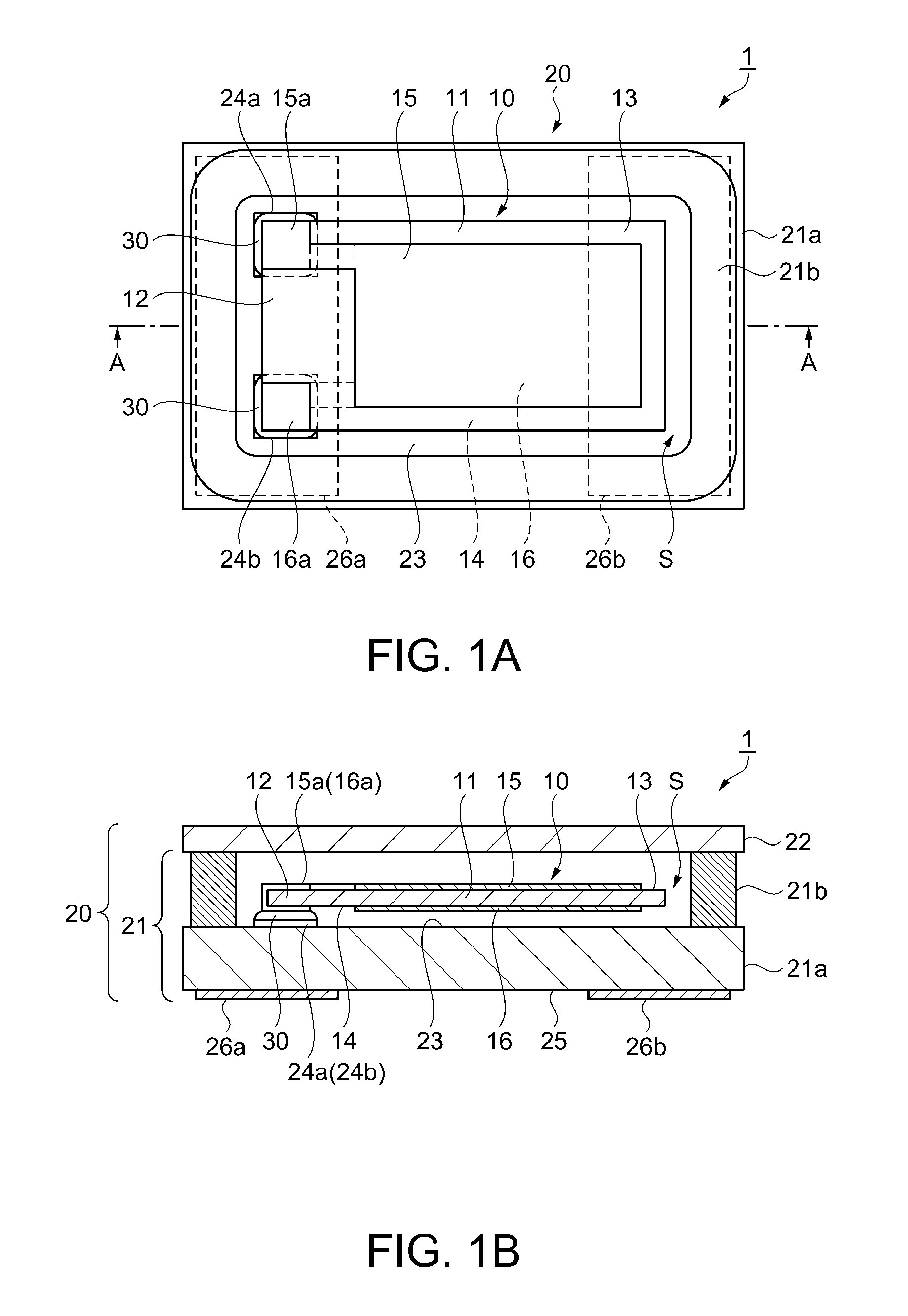
1. Technical Field The present invention relates to a package base, a package, an electronic device including this package, and an electronic apparatus and a moving object including this electronic device. 2. Related Art As a technique concerning bonding of a ceramic substrate relevant to a package base serving as a main body part of a package which is a constituent element of an electronic device and houses an electronic component, there has been known a production method, in which a bonding paste containing an active metal-containing brazing filler metal is applied onto a ceramic substrate, the ceramic substrate and a metal plate are placed in a stacked manner, and thereafter, both members are bonded to each other by a heat treatment, and then, an unnecessary portion of the metal plate is removed by an etching treatment, whereby a ceramic wiring board having a desired wiring pattern is obtained (see, for example, JP-A-8-46325). In the ceramic wiring board produced by the above production method, as the bonding paste containing an active metal-containing brazing filler metal, specifically, a bonding paste containing a Ti—Ag—Cu alloy obtained by blending Ti (titanium) which is an active metal in a metal having an Ag (silver)-Cu (copper) eutectic composition is used. It is believed that according to this, in the ceramic wiring board, the bonding strength between the ceramic substrate and a metal plate is improved, and thus, excellent thermal shock resistance and high reliability are obtained. When the above bonding paste is applied to, for example, a package (container) to be used for an electronic device or the like, it is necessary to bond a ceramic substrate (corresponding to a package base) and a metal plate (corresponding to a lid) to each other with a gap in the thickness direction through the bonding paste applied in a frame shape in plan view and to form an internal space for housing an electronic component or the like between the ceramic substrate and the metal plate. However, the above bonding paste has relatively high fluidity, and therefore has a problem that it easily spreads to the periphery even if it is applied in a predetermined shape, and lacks a shape retention property for retaining the predetermined shape (in other words, the ratio of the height relative to the application width is small). As a result, in the case of a package using the above bonding paste, in order to ensure the height of the internal space, when the bonding paste is applied, a reasonable application space including a space where the paste may spread is needed, and therefore, it may be difficult to further reduce the size. An advantage of some aspects of the invention is to solve at least a part of the problems described above, and the invention can be implemented as the following forms or application examples. This application example is directed to a package base including: a substrate containing a ceramic; and a bonding metal layer provided in a frame shape or a ring shape in plan view on the substrate, wherein the bonding metal layer contains a Ti—Ag—Cu-containing alloy and a metal belonging to Group 6 in the periodic table. According to this application example, the package base is configured such that the bonding metal layer (corresponding to a bonding paste) contains a Ti—Ag—Cu-containing alloy and a metal belonging to Group 6 in the periodic table, and therefore, by the physical properties of the metal belonging to Group 6, the shape retention property of the bonding metal layer can be improved. As a result, in the package base, the application width of the bonding metal layer can be decreased as compared with the configuration of the related art (for example, JP-A-8-46325), and thus, the planar size thereof can be reduced by that much. Accordingly, the package base can contribute to further reduction in the size of a package. In the package base according to the application example described above, it is preferred that the bonding metal layer contains Mo or W as the metal belonging to Group 6. According to this application example, the package base is configured such that the bonding metal layer contains Mo (molybdenum) or W (tungsten) as the metal belonging to Group 6, and therefore, by the physical properties of Mo or W having a higher melting point than Ti, Ag, and Cu, the shape retention property of the bonding metal layer can be further improved. In the package base according to the application example described above, it is preferred that the package base further includes a metal coating film covering at least a part of the surface of the bonding metal layer. According to this application example, the package base includes a metal coating film covering at least a part of the surface of the bonding metal layer, and therefore, oxidation of the bonding metal layer is suppressed, and the bonding strength between the substrate and a bonding target member to be bonded to each other through the bonding metal layer can be improved. In the package base according to the application example described above, it is preferred that the metal coating film includes a Ni film and a Au film which are stacked in this order from the bonding metal layer side. According to this application example, the package base is configured such that the metal coating film includes a Ni film and a Au film which are stacked in this order from the bonding metal layer side, and therefore, the metal coating film closely adheres to the bonding metal layer so that oxidation of the bonding metal layer can be reliably suppressed. This application example is directed to a package including: a substrate containing a ceramic; a lid covering one side of the substrate; and a bonding metal layer provided in a frame shape or a ring shape in plan view and bonding the substrate and the lid to each other to form an internal space, wherein the bonding metal layer contains Ti, Ag, Cu and a metal belonging to Group 6 in the periodic table. According to this application example, the package is configured such that the bonding metal layer contains a Ti—Ag—Cu-containing alloy and a metal belonging to Group 6 in the periodic table, and therefore, by the physical properties of the metal belonging to Group 6, the shape retention property of the bonding metal layer can be improved. As a result, in the package, the application width of the bonding metal layer can be decreased as compared with the configuration of the related art (for example, JP-A-8-46325) when forming an internal space, and thus, the planar size thereof can be reduced by that much. Accordingly, the size thereof can be further reduced. In the package according to the application example described above, it is preferred that the bonding metal layer contains Mo or W as the metal belonging to Group 6. According to this application example, the package is configured such that the bonding metal layer contains Mo or W as the metal belonging to Group 6, and therefore, by the physical properties of Mo or W having a higher melting point than Ti, Ag, and Cu, the shape retention property of the bonding metal layer can be further improved. In the package according to the application example described above, it is preferred that in the bonding metal layer, when the amount of Ti, Ag, and Cu is represented by A wt % and the amount of Mo is represented by B wt %, the ratio of A to B satisfies the following relational formula: 65≦A<100:35≧B>0 (provided that A+B=100). According to this application example, the package is configured such that in the bonding metal layer, when the amount of Ti, Ag, and Cu is represented by A wt % and the amount of Mo is represented by B wt %, the ratio of A to B satisfies the following relational formula: 65≦A<100:35≧B>0 (provided that A+B=100), and therefore, the shape retention property of the bonding metal layer can be improved while maintaining the wettability thereof to the substrate due to the blending ratio of Mo. In the package according to the application example described above, it is preferred that in the bonding metal layer, when the amount of Ti, Ag, and Cu is represented by A wt % and the amount of Mo is represented by B wt %, the ratio of A to B satisfies the following relational formula: 65≦A≦75:35≧B≧25 (provided that A+B=100). According to this application example, the package is configured such that in the bonding metal layer, when the amount of Ti, Ag, and Cu is represented by A wt % and the amount of Mo is represented by B wt %, the ratio of A to B satisfies the following relational formula: 65≦A≦75:35≧B≧25 (provided that A+B=100), and therefore, the shape retention property of the bonding metal layer can be further improved while maintaining the wettability thereof to the substrate due to the blending ratio of Mo. In the package according to the application example described above, it is preferred that the package further includes a metal coating film covering at least a part of the bonding metal layer. According to this application example, the package includes a metal coating film covering at least a part of the bonding face between the bonding metal layer and the lid, and therefore, oxidation of the bonding metal layer is suppressed, and the bonding strength between the substrate and the lid to be bonded to each other through the bonding metal layer can be improved. In the package according to the application example described above, it is preferred that the metal coating film includes a Ni film and a Au film which are stacked in this order from the bonding metal layer side. According to this application example, the package is configured such that the metal coating film includes a Ni film and a Au film which are stacked in this order from the bonding metal layer side, and therefore, the metal coating film closely adheres to the bonding metal layer so that oxidation of the bonding metal layer can be reliably suppressed. In the package according to the application example described above, it is preferred that the substrate has a recess on the lid side. According to this application example, the package is configured such that the substrate has a recess on the lid side, and therefore, for example, a housing target material such as an electronic component can be housed in the recess. Accordingly, in the package, as the lid, a lid in a flat plate shape which is easily processed can be used. In the package according to the application example described above, it is preferred that the lid has a recess on the substrate side. According to this application example, the package is configured such that the lid has a recess on the substrate side, and therefore, for example, a housing target material such as an electronic component can be housed in the recess. Accordingly, in the package, as the substrate, a substrate in a flat plate shape which is easily processed can be used. Further, in the case where the package is configured such that each of the substrate and the lid has a recess, for example, a housing target material such as an electronic component having a relatively large height can be housed across both recesses. This application example is directed to an electronic device including: the package according to any one of the application examples described above; and an electronic component, wherein the electronic component is housed in the internal space of the package. According to this application example, the electronic device having this configuration is configured such that an electronic component is housed in the internal space of the package having a reduced size according to any one of the above application examples, and therefore, an electronic device having a reduced size can be provided. This application example is directed to an electronic apparatus including the electronic device according to the application example described above. According to this application example, the electronic apparatus having this configuration includes the electronic device having a reduced size according to the above application example, and therefore, an electronic apparatus in which the size of a relevant component is reduced and the reliability is high can be provided. This application example is directed to a moving object including the electronic device according to the application example described above. According to this application example, the moving object having this configuration includes the electronic device having a reduced size according to the above application example, and therefore, a moving object in which the size of a relevant component is reduced and the reliability is high can be provided. The invention will be described with reference to the accompanying drawings, wherein like numbers reference like elements. Hereinafter, embodiments embodying the invention will be described with reference to the drawings. First, a quartz crystal resonator will be described as an example of an electronic device. As shown in The quartz crystal resonator element 10 is, for example, configured to integrally include a vibrating section 11, which is an AT-cut type in a flat plate shape cut out at a predetermined angle from quartz crystal ore or the like, has an approximately rectangular planar shape, and is excited to undergo thickness shear vibration, and a base section 12 which is connected to the vibrating section 11. In the quartz crystal resonator element 10, extraction electrodes 15 The extraction electrode 15 The extraction electrode 16 The excitation electrodes 15 and 16 and the extraction electrodes 15 The package 20 includes a package base body 21 In the package 20, a package base 21 is configured to include the package base body 21 In the package base body 21 The bonding metal layer 21 To be more specific, the bonding metal layer 21 As an example, the bonding metal layer 21 The thus prepared bonding metal layer 21 Further, as shown in The Ni film 21 For the lid 22, a metal having a thermal expansion coefficient at around normal temperature close to that of the package base body 21 On a first main surface 23 which is a main surface of one side (the lid 22 side) of the package base body 21 In the quartz crystal resonator element 10, the extraction electrodes 15 In the quartz crystal resonator 1, one side (the first main surface 23 side) of the package base body 21 The hermetically sealed internal space S of the package 20 is in a vacuum state (a state in which the vacuum degree is high) in which the pressure is reduced, or a state in which an inert gas such as nitrogen, helium, or argon is filled. In both end portions in the longitudinal direction (the lateral direction in the drawing) of a second main surface 25 which is a main surface on the opposite side from the one side (the first main surface 23 side) of the package base body 21 The electrode terminals 26 The internal terminals 24 The quartz crystal resonator 1 may be configured such that an electrode terminal is placed at each of the four corners on the second main surface 25 side of the package base body 21 In the quartz crystal resonator 1, for example, by a driving signal to be applied through the electrode terminals 26 Here, evaluation results with respect to the blending ratio of the Ti—Ag—Cu-containing alloy to Mo in the bonding metal layer 21 In Examples 1 to 12, the above-described quartz crystal resonator 1 was used, and only the blending ratio of the Ti—Ag—Cu-containing alloy to Mo in the bonding metal layer 21 With respect to the quartz crystal resonator 1 of each of Examples 1 to 12, the following evaluation was performed. Incidentally, depending on the evaluation items, evaluation was performed for the package base 21 alone. The wettability of the bonding metal layer 21 The shape (height, expansion of width), the presence or absence of a crack, and the like after firing the bonding metal layer 21 The CI (crystal impedance) value of the quartz crystal resonator element 10 was measured as an alternative characteristic (the airtightness is lower as the CI value is higher), and the airtightness of the internal space S in the quartz crystal resonator 1 was evaluated at the following three levels: A: good, B: moderate, C: poor. The evaluation results based on the above evaluation items are shown in As shown in Further, in the case of Example 1, a variation σ (standard deviation) in the height of the bonding metal layer 21 It is considered that this is because the bonding metal layer 21 On the other hand, in the cases of Examples 2 to 6 in which Mo is contained in an amount of 10 to 35 wt %, although some have a shape retention property evaluated as moderate (B), the height of the bonding metal layer 21 In particular, in the cases of Examples 4 to 6 in which Mo is contained in an amount of 25 to 35 wt %, the evaluation results are good (A) with respect to all evaluation items of the wettability to the package base body 21 It is considered that this is because the bonding metal layer 21 On the other hand, in the cases of Examples 7 to 12 in which Mo is contained in an amount of 40 to 90 wt %, although the shape retention property is good (A), the wettability to the package base body 21 Incidentally, the same evaluation results as above have been obtained also by using W in place of Mo in the bonding metal layer 21 As described above, the quartz crystal resonator 1 of the first embodiment exhibits the following effects for each configuration category. First, the package base 21 is configured such that the bonding metal layer 21 As a result, in the package base 21, the application width of the bonding metal layer 21 Further, the package base 21 is configured such that the bonding metal layer 21 Further, the package base 21 includes the metal coating film 21 Further, the package base 21 is configured such that the metal coating film 21 Next, the package 20 is configured such that the bonding metal layer 21 As a result, in the package 20, the application width of the bonding metal layer 21 Further, the package 20 is configured such that the bonding metal layer 21 Further, the package 20 is configured such that in the bonding metal layer 21 Further, the package 20 is configured such that in the bonding metal layer 21 Further, the package 20 includes the metal coating film 21 Further, the package 20 is configured such that the metal coating film 21 Next, the quartz crystal resonator 1 is configured such that the quartz crystal resonator element 10 as an electronic component is housed in the internal space S of the package 20, and therefore, a quartz crystal resonator as an electronic device having a reduced size can be provided. Next, another configuration of a quartz crystal resonator as an electronic device will be described. The parts common to those in the first embodiment are denoted by the same reference numerals and a description thereof is omitted, and different parts from those of the first embodiment will be mainly described. As shown in In a package 120 of the quartz crystal resonator 2, a package base body 121 To be more specific, in the package 120, the package base body 121 According to this, in the package 120, the package base body 121 On a bottom surface 127 On a first main surface 123 of the second layer of the package base body 121 According to this, the package 120 of the quartz crystal resonator 2 is configured such that the package base body 121 Accordingly, in the package 120, as the lid 22, a lid in a flat plate shape which is easily processed can be used. Further, in the package 120, the shape retention property of the bonding metal layer 121 In the quartz crystal resonator 2, the quartz crystal resonator element 10 as an electronic component is housed in the internal space S of the package 120, and therefore, a quartz crystal resonator as an electronic device having a reduced size can be provided. Next, still another configuration of a quartz crystal resonator as an electronic device will be described. The parts common to those in the first embodiment are denoted by the same reference numerals and a description thereof is omitted, and different parts from those of the first embodiment will be mainly described. As shown in In a package 220 of the quartz crystal resonator 3, a lid 222 has a recess 227 on a package base body 21 To be more specific, in the package 220, the lid 222 is formed into a cap shape having the recess 227 depressed toward the upper side in the drawing and a flange section 228 extending from the entire periphery of the recess 227 along a first main surface 23 of the package base body 21 A bonding metal layer 221 According to this, in the package 220 of the quartz crystal resonator 3, the lid 222 has the recess 227 on the package base body 21 Accordingly, in the package 220, as the package base body 21 Further, in the package 220, the shape retention property of the bonding metal layer 221 In the quartz crystal resonator 3, the quartz crystal resonator element 10 as an electronic component is housed in the internal space S of the package 220, and therefore, a quartz crystal resonator as an electronic device having a reduced size can be provided. The above-described package may be configured such that each of the package base body and the lid has a recess. According to this, for example, a housing target material such as an electronic component having a relatively large height can be housed across both recesses. Next, a quartz crystal oscillator will be described as an example of an electronic device. The parts common to those in the first embodiment are denoted by the same reference numerals and a description thereof is omitted, and different parts from those of the first embodiment will be mainly described. As shown in To be more specific, in the package 320, a package base body 321 The internal connection terminals 327 The internal connection terminals 327 The IC chip 40 incorporating an oscillation circuit is fixed to the bottom surface 327 For the connection between the IC chip 40 and the internal connection terminals 327 In the quartz crystal oscillator 5, a driving signal is output from the oscillation circuit of the IC chip 40 by an external input, and the quartz crystal resonator element is excited to undergo thickness shear vibration and resonates (oscillates) at a predetermined frequency, amplifies a resonance signal (oscillation signal) thereof, and then, outputs the signal from, for example, the electrode terminals 26 As described above, in the quartz crystal oscillator 5, the shape retention property of the bonding metal layer 21 Accordingly, the quartz crystal oscillator 5 can provide a quartz crystal oscillator as an electronic device having a reduced size. Next, a cellular phone will be described as an example of an electronic apparatus including the above-described electronic device. A cellular phone 700 includes a quartz crystal resonator or a quartz crystal oscillator as an electronic device described in the above embodiments. The cellular phone 700 shown in The application of the electronic device such as the above-described quartz crystal resonator is not limited to the above-described cellular phone, and the electronic device can be favorably used as a timing device of an electronic apparatus including an electronic book, a personal computer, a television, a digital still camera, a video camera, a video recorder, a navigation apparatus, a pager, an electronic organizer, a calculator, a word processor, a workstation, a videophone, a POS terminal, a game instrument, a medical apparatus (for example, an electronic thermometer, a blood pressure meter, a blood sugar meter, an electrocardiogram measuring instrument, an ultrasound diagnostic instrument, and an electronic endoscope), a fish finder, various measurement apparatuses, gauges, a flight simulator, and the like. In any case, the effects described in the above embodiments are exhibited, and thus, an electronic apparatus in which the size of a relevant component is reduced and the reliability is high can be provided. Next, an automobile will be described as an example of a moving object including the above-described electronic device. An automobile 800 includes a quartz crystal resonator or a quartz crystal oscillator as an electronic device described in the above embodiments. The automobile 800 uses the above-described quartz crystal resonator (any of 1 to 3) or the above-described quartz crystal oscillator 5 as, for example, a timing device such as a reference clock oscillation source of various electronically controlled apparatuses (for example, an electronically controlled fuel injector, an electronically controlled ABS apparatus, an electronically controlled constant speed travelling apparatus, and the like) mounted therein. According to this, since the automobile 800 includes the above-described quartz crystal resonator or quartz crystal oscillator, the effects described in the above embodiments are exhibited, and thus, for example, the size of the respective electronically controlled apparatuses is reduced, and high reliability and excellent performance can be exhibited. The application of the electronic device such as the above-described quartz crystal resonator is not limited to the above-described automobile 800, and the electronic device can be favorably used as a timing device such as a reference clock oscillation source of a moving object including a self-propelled robot, a self-propelled conveying apparatus, a train, a ship, an airplane, a satellite, and the like. In any case, the effects described in the above embodiments are exhibited, and thus, a moving object in which the size of a relevant component is reduced and the reliability is high can be provided. The shape of the quartz crystal resonator element of the quartz crystal resonator is not limited to a flat plate shape shown in the drawing and may be a shape in which a central portion is thick and a peripheral portion is thin (for example, a convex shape, a bevel shape, or a mesa shape), or a reverse shape in which a central portion is thin and a peripheral portion is thick (for example, a reverse mesa shape), or the like, and also may be a tuning folk shape. The material of the resonator element is not limited to quartz crystal and may be a piezoelectric material such as lithium tantalate (LiTaO3), lithium tetraborate (Li2B4O7), lithium niobate (LiNbO3), lead zirconate titanate (PZT), zinc oxide (ZnO), or aluminum nitride (AlN), or a semiconductor material such as silicon (Si). The driving method for thickness shear vibration may be an electrostatic driving method employing a Coulomb's force other than a method employing a piezoelectric effect of a piezoelectric body. The Ti—Ag—Cu-containing alloy of the bonding metal layer is not limited to an alloy containing only Ti, Ag, and Cu, and may contain, for example, a metal which does not belong to Group 6 in the periodic table such as Sn (tin). The entire disclosure of Japanese Patent Application No. 2014-145667, filed Jul. 16, 2014 is expressly incorporated by reference herein. A package base includes a package base body and a bonding metal layer provided in a frame shape or a ring shape in plan view on the package base body, wherein the bonding metal layer contains a Ti—Ag—Cu-containing alloy and a metal belonging to Group 6 in the periodic table. 1. A package base, comprising:
a substrate containing a ceramic; and a bonding metal layer provided in a frame shape or a ring shape in plan view on the substrate, wherein the bonding metal layer contains a Ti—Ag—Cu-containing alloy and a metal belonging to Group 6 in the periodic table. 2. The package base according to 3. The package base according to 4. The package base according to 5. A package, comprising:
a substrate containing a ceramic; a lid covering one side of the substrate; and a bonding metal layer provided in a frame shape or a ring shape in plan view and bonding the substrate and the lid to each other to form an internal space, wherein the bonding metal layer contains Ti, Ag, Cu, and a metal belonging to Group 6 in the periodic table. 6. The package according to 7. The package according to 8. The package according to 9. The package according to 10. The package according to 11. The package according to 12. The package according to 13. An electronic device, comprising:
the package according to an electronic component, wherein the electronic component is housed in the internal space of the package. 14. An electronic apparatus comprising the electronic device according to 15. A moving object comprising the electronic device according to BACKGROUND
SUMMARY
APPLICATION EXAMPLE 1
APPLICATION EXAMPLE 2
APPLICATION EXAMPLE 3
APPLICATION EXAMPLE 4
APPLICATION EXAMPLE 5
APPLICATION EXAMPLE 6
APPLICATION EXAMPLE 7
APPLICATION EXAMPLE 8
APPLICATION EXAMPLE 9
APPLICATION EXAMPLE 10
APPLICATION EXAMPLE 11
APPLICATION EXAMPLE 12
APPLICATION EXAMPLE 13
APPLICATION EXAMPLE 14
APPLICATION EXAMPLE 15
BRIEF DESCRIPTION OF THE DRAWINGS
DESCRIPTION OF EXEMPLARY EMBODIMENTS
First Embodiment
Evaluation of Wettability to Package Base Body 21
Evaluation of Shape Retention Property (Evaluation of Appearance)
Evaluation of Airtightness
Evaluation Results
Second Embodiment
Third Embodiment
Fourth Embodiment
Electronic Apparatus
Moving Object