SCALABLE FIR FILTER
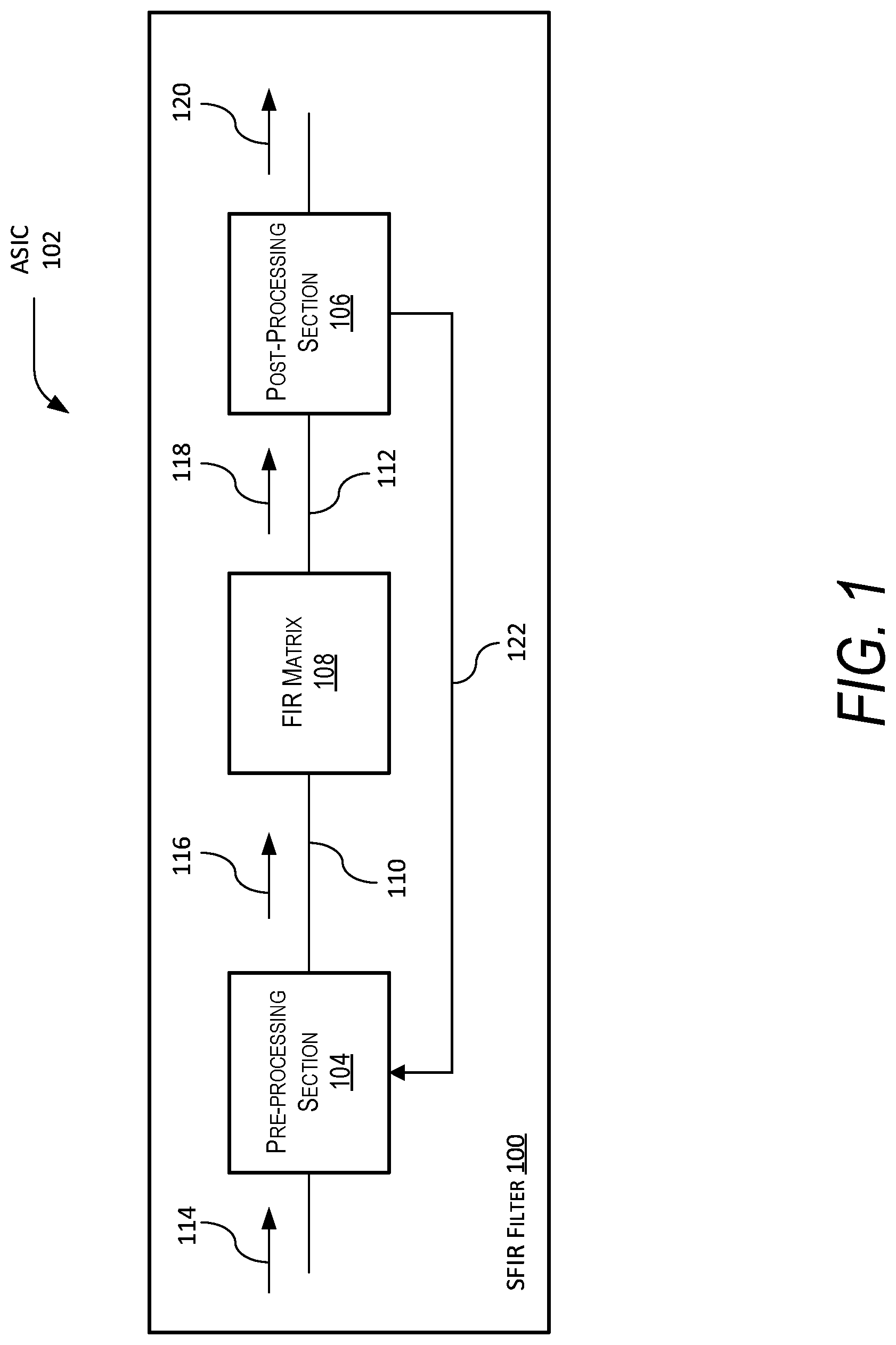
This invention was made with United States Government support. The government has certain rights in the invention. The present disclosure is related to filters, and more specifically, finite impulse response (“FIR”) filters. Digital filters are a key element in digital signal processing (“DSP”) applications, in particular any application that may transmit or receive a Radio Frequency (RF) signal. Moreover, Finite Impulse Response (“FIR”) Filters are a type of filter that is frequently used to perform matrix multiplication operations between input data and a set of coefficients. However, generally, the larger a filter becomes, the more difficult the filter becomes to manufacture when implemented in an Application Specific Integrated Circuit (“ASIC”) because of the number of required routes associated with the filter. Generally, software (e.g., processors) or hardware (e.g., ASICs or Field Programmable Gate Arrays [“FPGAs”]) approaches are utilized for DSP applications. Hardware approaches are generally utilized for intensive DSP applications that require pipelining to achieve high data rates. However, a problem with both ASIC and FPGA devices is that a significant amount of the die area of both are consumed by filtering resources. This is because DSP applications typically involve a significant amount of filtering that may be estimated as needing approximately half the resources in a given application. The problem with software approaches is that software solutions have difficulty with computational intensive DSP applications such as, for example, streaming data. Known hardware approaches are more suitable for these types of DSP applications but have varying problems with flexibility, efficiency, costs, size, weight, and power. Specifically, the problem with ASICs is that they are integrated circuits that are fabricated from a predetermined design that is designed to perform a specific application. As such, they are efficient but traditionally inflexible because, again, they are designed and fabricated to perform very specific applications and do not have the flexibility to perform other functions or applications. Because of this limitation, they have high non-recurring engineering (“NRE”) costs in both the design and fabrication processes. Unlike ASICs, FPGAs are flexible in operation because they may be programmed to perform different functions and applications. However, this flexible comes at a cost in high physical size and weight of the die and high power costs known as SWAP (size, weight, and power). As such, FPGAs are flexible but inherently inefficient. Therefore, there is a need for a FIR filter design that is flexible, cost effective (i.e., has low NRE costs), and efficient (i.e., low SWAP). Disclosed is a Scalable Finite Impulse Response (“SFIR”) filter. The SFIR filter includes a pre-processing section, a post-processing section, and a finite impulse response (“FIR”) filtering matrix. The FIR Matrix includes a plurality of filter taps and a plurality of signal paths in signal communication with each filter tap. The plurality of signal paths are arranged to allow re-configurable data throughput between the each filter tap and the pre-processing module and post-processing module are in signal communication with the FIR Matrix. Further disclosed is an Application Specific Integrated Circuit (“ASIC”). The ASIC includes the SFIR filter, where the SFIR filter includes the pre-processing section, the post-processing section, and the FIR Matrix. The FIR Matrix again includes the plurality of filter taps and the plurality of signal paths in signal communication with each filter tap, where the plurality of signal paths are arranged to allow re-configurable data throughput between the each filter tap. The pre-processing module and post-processing module are in signal communication with the FIR Matrix and the number of filter taps of the plurality of filter taps is predetermined. Other devices, apparatus, systems, methods, features, and advantages of the disclosure will be or will become apparent to one with skill in the art upon examination of the following figures and detailed description. It is intended that all such additional systems, methods, features, and advantages be included within this description, be within the scope of the disclosure, and be protected by the accompanying claims. The disclosure may be better understood by referring to the following figures. The components in the figures are not necessarily to scale, emphasis instead being placed upon illustrating the principles of the disclosure. In the figures, like reference numerals designate corresponding parts throughout the different views. A Scalable Finite Impulse Response (“SFIR”) filter is disclosed. The SFIR filter includes a pre-processing section, a post-processing section, and a finite impulse response (“FIR”) filtering matrix. The FIR Matrix includes a plurality of filter taps and a plurality of signal paths in signal communication with each filter tap. The plurality of signal paths are arranged to allow re-configurable data throughput between the each filter tap and the pre-processing module and post-processing module are in signal communication with the FIR Matrix. Further disclosed is an Application Specific Integrated Circuit (“ASIC”). The ASIC includes the SFIR filter, where the SFIR filter includes the pre-processing section, the post-processing section, and the FIR Matrix. The FIR Matrix again includes the plurality of filter taps and the plurality of signal paths in signal communication with each filter tap, where the plurality of signal paths are arranged to allow re-configurable data throughput between the each filter tap. The pre-processing module and post-processing module are in signal communication with the FIR Matrix and the number of filter taps of the plurality of filter taps is predetermined. Specifically, in In an example, of operation, the SFIR filter 100 receives an input digital signal 114 at the pre-processing section 104 that processes and organizes the data in the input digital signal 114 in an arranged order that is passed to FIR Matrix 108 via input matrix signal 116 along the signal path 110. The FIR Matrix 108 receives and filters the input matrix signal 116 and to produce an intermediate filtered output signal 118 that is passed to the post-processing section 106 via the signal path 112. The post-processing section 106 receives the intermediate filtered output signal 118 and processes and organizes the data in the intermediate filtered output signal 118 to produce the filtered output signal 120 that is passed to other devices, components, circuitry, or modules in the ASIC 102. The SFIR filter 100 also includes a loopback signal path 122 that is from the post-processing section 106 to the pre-processing section 104. In For ease of illustration, in this example, only 16 filter taps 202 As will be described later, by re-configuring the data throughput between the different filter taps 202 Also for ease of illustration, in this example, each filter tap is shown having a pair of input terminals 214 and pair of output terminals 216 in signal communication with the respective signal paths of the plurality of signal paths 204, 206, 208, 210, and 212. Specifically, in this example, the pair of input terminals 214 and pair of output terminals 216 are shown with regard to filter tap 202 When combined with the pre-processing section 104 and post-processing section 106, the FIR Matrix 200 allow the SFIR filter 100 to be configured as different types of digital filters such as, for example, a Hilbert transform filter, decimator, interpolator, real FIR filter (i.e., a real value filter that is not a complex filter), complex FIR filter, or adaptive filter. As an example, for real FIR filter (i.e., a non-complex FIR filter), the SFIR filter 100 may include the pre-processing section configured 104 as a first pass-through device and the post-processing section 106 configured as a second pass-through device. Alternatively, in a complex FIR filter, the SFIR filter 100 includes the pre-processing section 104 configured as a fan-out device and the post-processing section 106 configured as a summation device. If, instead, the SFIR filter 100 is configured as a decimator, the SFIR filter 100 includes the pre-processing section 104 configured as a re-order device and the post-processing section 106 configured as a summation device. Moreover, if the SFIR filter 100 is configured as an interpolator, the interpolator includes the pre-processing section 104 configured as a fan-out device and the post-processing section 106 configured as a re-order device. It is appreciated by those skilled in the art that the circuits, components, modules, and/or devices of, or associated with, the SFIR filter 100 and ASIC 102 are described as being in signal communication with each other, where signal communication refers to any type of communication and/or connection between the circuits, components, modules, and/or devices that allows a circuit, component, module, and/or device to pass and/or receive signals and/or information from another circuit, component, module, and/or device. The communication and/or connection may be along any signal path between the circuits, components, modules, and/or devices that allows signals and/or information to pass from one circuit, component, module, and/or device to another and includes wireless or wired signal paths. The signal paths may be physical, such as, for example, conductive wires, electromagnetic wave guides, cables, attached and/or electromagnetic or mechanically coupled terminals, semi-conductive or dielectric materials or devices, or other similar physical connections or couplings. Additionally, signal paths may be non-physical such as free-space (in the case of electromagnetic propagation) or information paths through digital components where communication information is passed from one circuit, component, module, and/or device to another in varying digital formats without passing through a direct electromagnetic connection. Turning to In this example, the first output terminal 304 of the filter tap 202 The second output terminal 332 of the filter tap 202 The accumulator output 308 of the filter tap 202 In general and as will be discussed later, in this example, each filter tap 202 It is appreciated by those of ordinary skill in the art that parallel digital filters are usually utilized to process even number of parallel paths. As such, in this example, the plurality of signal paths 206 are show communicating with an even number of paths such as filter tap 202 In this example, the first output terminals 304, 326, 328, and 330 and second output terminals 306, 332, 334, and 336 produce the same signal with the difference that the second output terminals 306, 332, 334, and 336 produce that same signal delayed in time versus the signal produced at the first output terminals 304, 326, 328, and 330. In other words, the signals produced at the first output terminals 304, 326, 328, and 330 may be represented as xn(t) while the signals produced at the second output terminals 306, 332, 334, and 336 may be represented as xn(t+1), where x represent the signal, n represents the parallel path, and t represent time. In general, in this example, there is no need to connect the delayed signal in the top row (i.e., second output terminal 306 of filter tap 202 In In Utilizing the design of the SFIR filter 100 on an ASIC 102, the SFIR filter 100 may be fabricated with an arbitrary filter length (i.e., an arbitrary number of filter taps) or real-time data throughput (i.e., the number of parallel inputs and outputs). Once fabricated, the same filter structure may be re-configured to handle differ data inputs such that, for example, the SFIR filter 100 may be re-configured to filter a small number of fat pipes or a large number of thin pipes. Likewise, the same filter structure may be re-configured to perform different filter operations such that, for example, the SFIR filter 100 may be reconfigured to provide a high number of filter taps for a low aggregate data rate, or a low number of filter taps for a high aggregate data rate. In general, interconnects formed by the plurality of signal paths 204, 206, 208, 210, and 212 between the multiplexers (in the filter taps) allow the SFIR filter 100 to be re-configured. Turning to In these examples, the filter coefficients are preferably configurable by a user instead of being hard coded. They may be implemented, for example, utilizing registers and/or flip-flops that may be configurable by loading the registers and/or flip-flops utilizing a Network-on-Chip communication subsystem or other type of system. In this example, the multiplexer 502 is in signal communication with the first delay element 504 via signal path 516. The gain section multiplier 512 is in signal communication with the first delay element 504, coefficient section 514, and adder 510 via signal paths 518, 520, and 522, respectively. Furthermore, the multiplexer 502 is in signal communication with the plurality of input terminals 524, the second delay element 508 is in signal communication with the accumulation input 526, the output of the multiplexer 502 is in signal communication with the first output terminal 528, the output of the first delay element 504 is in signal communication with the second output terminal 530, and the adder 510 is in signal communication with accumulator output 532. In this example, the plurality of input terminals 524 (referred to as “mux-in”), first output terminal 528 (referred to as “mux-out”), and second output terminal 530 (referred to as “mux-out-dly”) are the input to and the undelayed output of the multiplexer 502, respectively. Turning back to Assuming that a number P represents the number of parallel path configurations in the filter tap 500, the total number of inputs to any multiplexer (e.g., the mux-in plurality of input terminals 524 to multiplexer 502) will be determined by P, where P is a non-zero positive integer equal to 1 or greater. If [(M+1)mod P]=0, then mux_in (M, N)=mux_out (M−P+1, N−1), else mux_in (M, N)=mux_out (M+1, N−1). It is appreciated by those of ordinary skill in the art that the examples described in this disclosure are examples that utilize an even number (i.e., 2n) of taps and parallel paths. This has been done for simplicity of illustration but it is appreciated that the examples given will also be applicable to non-even number of taps and parallel paths since the FIR design described will be applicable to any height and width combination. In As discussed before, the multiplexer 602 is in signal communication with the first delay element 604 via signal path 516. The gain section multiplier 612 is in signal communication with the first delay element 604, coefficient section 614, and adder 610 via signal paths 618, 620, and 622, respectively. Furthermore, the multiplexer 602 is in signal communication with the plurality of input terminals 624, the second delay element 608 is in signal communication with the accumulation input 626, the output of the multiplexer 602 is in signal communication with the first output terminal 628, the output of the first delay element 604 is in signal communication with the second output terminal 630, and the adder 610 is in signal communication with accumulator output 632. However, in this example, the first delay element 604, the second delay element 608, and coefficient section 614 are D-type flip-flops that act as data latches, where they hold or remember the data present on their data input (the “D” input shown). D-type flip-flops generally act as one-bit data latches that pass their data input based on their clock inputs. In the present disclosure, the D-type flip-flops are generally implemented as multi-bit registers. It is appreciated by those of ordinary skill in the art other types of flip-flops (such as, for example, J-K or R-S flip-flops) may also be utilized with the appropriate circuitry to support data latching. The utilization of D-type flip-flops for the first delay element 604, the second delay element 608, and coefficient section 614 within each filter tap (i.e., every stage) of the SFIR filter 100 allow the design of the SFIR filter 100 to be scaled up to any size FIR filter desired. Additionally, the D-type flip-flops reduce routing congestion between filter taps and do not slow down the clock speeds of various configured filters within the SFIR filter 100. The D-type flip-flops for first delay element 604 and the second delay element 608 add pipelining to the ASIC 102 that allows the SFIR filter 100 to operate much quicker than known FIR techniques utilizing multiple filter taps. Specifically, the D-type flip-flops for first delay element 604 and the second delay element 608 pipelines the accumulator path (i.e., from the first delay element 604 through the gain section multiplier 612 to the adder 610) so that the maximum logic states crosses between registered elements (i.e., filter taps) is always just one multiplier and one adder. This maintains the maximum data throughput for any configured filter length. Furthermore, in a parallel filter design of the SFIR filter 100, each registered data input goes to only one multiplier regardless of filter size or configuration without having to fan-out to different multipliers as in traditional filter designs. The SFIR filter 100, as disclosed, includes built-in pipelining such that the input and output of each filter tap is in signal communication to each multiplier. This point-to-point approach allows the SFIR filter 100 to route and maintain a high achievable clock speed even as the SFIR filter 100 grows in size. In this example, for ease of illustration and simplicity, the flip-flop implementation is shown as one-bit data latches; however, it is appreciated by those of ordinary skill in the art that in practice the flip-flops will likely be implemented as multi-bit data latches. Moreover, in practice the adder 610 may be implemented by a plurality of adders and the gain section multiplier 612 may be implemented as a plurality of gain section multipliers. In this example, the data width of the first delay element 604 and coefficient section 614 are user defined and the data width of the second delay element 608 is driven by the bit growth through the plurality of gain section multipliers (that includes gain section multiplier 612) and the plurality of adders (that includes adder 610). Typically, the input data path through the plurality of input terminals 624, multiplexer 602, signal path 516 and first delay element 604 will be driven by a signal source such as, for example, an analog-to-digital converter (“ADC”). The coefficient section 614 will be driven by the needed filter performance, which usually needs more bits for higher performance of the filter. The accumulation path through the second delay element 608 has a data width that is equal to the data width of the first delay element 604 plus the data width of the coefficient section 614 and the base 2 logarithm (“log 2”) of the number of filter taps. As an example, if the SFIR filter 100 has an 8 bit data input, 16 bit coefficients, and 16 filter taps, the data width of second delay element 608 will be equal to 8 plus 16 plus 4 that equals 28. In As discussed before, the multiplexer 702 is in signal communication with the first delay element 704 via signal path 716. The gain section multiplier 712 is in signal communication with the first delay element 704, coefficient section 714, and adder 710 via signal paths 718, 720, and 722, respectively. Furthermore, the multiplexer 702 is in signal communication with the plurality of input terminals 724, the second delay element 708 is in signal communication with the accumulation input 726, the output of the multiplexer 702 is in signal communication with the first output terminal 728, the output of the first delay element 704 is in signal communication with the second output terminal 730, and the adder 710 is in signal communication with accumulator output 732. Similar to the example in relation to In this example, the first output terminal 628 of the first filter tap 600 is in signal communication with multiplexer 702 of the second filter tap 700 via a signal path 734 and one of the terminals of the plurality of input terminals 724. Additionally, the accumulator output 632 of the first filter tap 600 is in signal communication with the second delay element 708 of the second filter tap 700 through the signal path 736 and the accumulator input 726. In other words, the signal path 736 is a first adder signal path from the adder 610 (i.e., a first filter tap adder) to the second delay element 708 (i.e., the second filter tap second flip-flop). In an example of operation, the D-type flip-flop of the first delay element 604 of the first tap 600 produces a data value 738 at the Q-output that is multiplied, at the gain section multiplier 612, with a coefficient value 740 to produce filter output value 742 that is combined in the adder 610 with any previous accumulation value 744 to produce an accumulation value 746 that is passed to the input 748 of the D-input of the D-type flip-flop of the second delay element 708 of the second filter tap 700 via the accumulator input 726. The process would repeat to any other filter taps that are in signal communication with accumulator output 732 of the second filter tap 700. Turning to In this example, the following tables (Tables 1 through 6) of filter element values for FIR Matrix 800 performing four parallel processing paths are described for five clock cycles (i.e., clock cycles 0 through 5). Additionally, in this example, the following signal path connections are assumed. The first output terminal 806 The first output terminal 806 The first output terminal 806 The first output terminal 806 In this example, the x value outputs (i.e., xout) of the last filter tap (i.e., filter taps 812 It is appreciated by those of ordinary skill in the art that the general relationship for a FIR filter is described as follows: where the value xn is the input values to the FIR filter, N is the filter order (i.e., designates the total number of filter taps), ci is the impulse response at ith instant for 0≤i≤N of the Nth order FIR filter that corresponds to the FIR filter coefficient values, and yn is the output value of the FIR filter. In this example, values x0 through x19 are the FIR Matrix 800 filter input values, the values xi represent the sequential samples in time of the same data stream where, in this example, the data throughput of the FIR filter is four samples per clock, and the values c0 through c3 are the filter coefficient values. For simplicity, only values x0 through x19 are called out in the tables below. As described earlier, the variable xout is the value of the first delay element in the last filter tap in the parallel paths (i.e., filter taps 812 Turning to In As described in relation to It is appreciated that the column values of the filter coefficients are the same for the four paths since the SFIR filter 900 is configured as a real value parallel FIR filter having four parallel paths. As such, the filter coefficients C0 1002 In The filter input x(n) 1126 is input into the pre-processing section 1104, where the filter input x(n) 1126 includes a filter input real component xre(n) 1128 and a filter input imaginary component xim(n) 1130 because in this example the filter input x(n) 1126 is a complex data signal. The filter input real component xre(n) 1128 is passed to the FIR Matrix 1108 via signal paths 1110 and 1112 and the filter input imaginary component xim(n) 1130 is passed to the FIR Matrix 1108 via signal paths 1114 and 1116. The FIR Matrix 1108 is configured as a complex value FIR filter having four FIR sub-filters 1132, 1134, 1136, and 1138 having transfer functions of hre(n) and him(n), respectively. In this example, the FIR sub-filter 1132 receives the filter input real component xre(n) 1128, filters it, and outputs a first portion of a filter output that is passed to a first adder 1140 within the post-processing section 1106. Simultaneously, the FIR sub-filter 1136 receives the filter input imaginary component xim(n) 1130, filters it, and outputs a second portion of the filter output that is passed to the first adder 1140. The second portion of a filter output may be complemented (i.e., converted into an opposite value) within the post-processing section 1106 so as to cause the first adder 1140 to subtract the second portion of the filter output from the first portion of the filter output to produce a filter output real component yre(n) 1142. Moreover, the FIR sub-filter 1134 receives the filter input real component xre(n) 1128, filters it, and outputs an third portion of a filter output that is passed to a second adder 1144 within the post-processing section 1106. Simultaneously, the FIR sub-filter 1138 receives the filter input imaginary component xim(n) 1130, filters it, and outputs an fourth portion of the filter output that is passed to the second adder 1144. The second adder 1144 adds the third portion of the filter output to the fourth portion of the filter output to produce a filter output imaginary component yim(n) 1146. The filter output real component and filter output imaginary component may be combined in a single complex data signal referred to as filter output y(n) 1148. In In this example, the SFIR filter 1100 receives two complex input signal that are input into the pre-processing section 1104 as four real value input signals herein referred to as a first real input xre(0) 1202 and a second real input xre(1) 1204 and a first imaginary input xim(0) 1206 and an imaginary phase input xim(1) 1208. These signals are re-ordered and fanned out by the pre-processing section 1104 and feed into the FIR Matrix 1108, where the first real input xre(0) 1202 is input into the filter taps 1200 The FIR Matrix 1108 then produces the intermediate outputs zii(0) 1210, zii(1) 1212, ziq(0) 1214, ziq(1) 1216, zqq(0) 1218, zqq(1) 1220, zqi(0) 1222, and zqi(1) 1224 that are passed to the post-processing section 1106. For simplicity of illustration, the subscript notation of the variables z have been changed to “i” for real instead of “re” and “q” for imaginary for “im,” since placing subscripts “im” and “re” or “re” and “im” would be confusing. As such, the subscripts for the variable z will be “zii” instead of “zrere,” “ziq” instead of “zreim,” “zqi” instead of “zimre,” and “zqq” instead of “zimim.” As such, the post-processing section 1106 then combines the intermediate outputs zii(0) 1210 with zqq(0) 1218 at a first adder 1226 to produce a first complex filter output signal yre(0) 1228 and zii(1) 1212 with zqq(1) 1220 at a second adder 1230 to produce a second complex filter output signal yim(0) 1232. In this example, the intermediate outputs zqq(0) 1218 and zqq(1) 1220 may be complimented to produce opposite values such that the first adder 1226 and second adder 1230 produce subtractions between zii(0) 1210 with zqq(0) 1218 and yre(0) 1228 and zii(1) 1212, respectively. Furthermore, the post-processing section 1106 then also combines the intermediate outputs ziq(0) 1214 with zqi(0) 1222 at a third adder 1234 to produce a third complex filter output signal yre(1) 1236 and combines the intermediate ziq(1) 1216 with zqi(1) 1224 at a fourth adder 1238 to produce a fourth complex filter output signal yq(1) 1240. In In this example, the pre-processing section 1302 receives the filter input x(n) 1320. The pre-processing section 1302 is configured, in this example, as a distribution network 1322 that re-orders the filter input x(n) 1320 and feeds the FIR sub-filters 1324, 1326, and 1328, respectively. The FIR sub-filters 1324, 1326, and 1328 have the corresponding transfer functions H0(n), H1(n), and HD-1(n), where D represents the number of FIR sub-filters present in the FIR Matrix 1306. In this example, the first FIR sub-filter 1324 is in signal communication with the distribution network 1322 via signal path 1308, the second FIR sub-filter 1326 is in signal communication with the distribution network 1322 via signal path 1310, and the third FIR sub-filter 1328 is in signal communication with the distribution network 1322 via signal path 1312. The post-processing section 1304 is configured as a summation network 1330 that adds the outputs of the FIR sub-filters 1324, 1326, and 1328. The first FIR sub-filter 1324 is in signal communication with the summation network 1330 via signal path 1314, the second FIR sub-filter 1326 is in signal communication with the summation network 1330 via signal path 1316, and the third FIR sub-filter 1328 is in signal communication with the summation network 1330 via signal path 1318. In an example of operation, the first FIR sub-filter 1324 receives a filter input from the distribution network 1322, filters it, and outputs a first portion of a filter output that is passed to the summation network 1330. Simultaneously: the second FIR sub-filter 1326 receives a filter input from the distribution network 1322, filters it, and outputs a first portion of a filter output that is passed to the summation network 1330; and the third FIR sub-filter 1328 receives a filter input from the distribution network 1322, filters it, and outputs a first portion of a filter output that is passed to the summation network 1330. The outputs from the FIR sub-filters 1324, 1326, and 1328 are received by the summation network 1330 and combined (i.e., added together) to produce a filter output y(n/D) 1332, where the filter input x(n) 1320 has n number of inputs and the filter output y(n/D) 1332 has n/D outputs. As such, in this example, the n number of inputs in the filter input x(n) 1320 are decimated into n/D outputs of the filter output y(n/D) 1332. In In this example, the SFIR filter 1300 receives the filter input x(n) 1320 that is input into the pre-processing section 1302 as eight input signals herein referred to as first input signal x(0) 1402, second input signal x(1) 1404, third input signal x(2) 1406, fourth input signal x(3) 1408, fifth input signal x(4) 1410, sixth input signal x(5) 1412, seventh input signal x(6) 1414, and eighth input signal x(7) 1415. These signals are re-ordered by the pre-processing section 1302 and input into the FIR Matrix 1306, where the first input signal x(0) 1402 is input into the filter tap 1400 The FIR Matrix 1306 then produces the intermediate outputs z(0) 1416, z(1) 1418, z(2) 1420, z(3) 1422, z(4) 1424, z(5) 1426, z(6) 1428, and z(7) 1430 that are passed to the post-processing section 1106. As such, the post-processing section 1304 then combines the intermediate outputs z(0) 1416 with z(4) 1424 at a first adder 1432 to produce a first output signal y(0) 1434 and z(1) 1418 with z(5) 1426 at a second adder 1436 to produce an output signal y(1) 1438. Moreover, the intermediate outputs z(2) 1420 and z(6) 1428 at a third adder 1440 to produce a third output signal y(2) 1442 and the intermediate outputs z(3) 1422 and z(7) 1430 at a fourth adder 1444 to produce a fourth output signal y(3) 1446. In In this example, the pre-processing section 1502 receives the filter input x(n) 1520. The pre-processing section 1502 is configured to fan out the filter input x(n) 1520 and feed the FIR sub-filters 1522, 1524, and 1526, respectively. The FIR sub-filters 1522, 1524, and 1526 have the corresponding transfer functions H0(n), H1(n), and HI-1(n), where I represents the number of FIR sub-filters present in the FIR Matrix 1306. The post-processing section 1504 is configured to operate as a distribution network 1528. In this example, the first FIR sub-filter 1522 is in signal communication with the distribution network 1528 via signal path 1514, the second FIR sub-filter 1524 is in signal communication with the distribution network 1528 via signal path 1516, and the third FIR sub-filter 1526 is in signal communication with the distribution network 1528 via signal path 1518. The distribution network 1528 distributes and re-orders the intermediate filter outputs of the FIR sub-filters 1522, 1524, and 1526 to produce the filter outputs y0(n) 1530, y1(n) 1532, and yI-1(n) 1534. In an example of operation, the first FIR sub-filter 1522 receives a filter input from pre-processing section 1502, filters it, and outputs an intermediate filter output that is passed to the distribution network 1528. Simultaneously: the second FIR sub-filter 1524 receives a filter input from the from pre-processing section 1502, filters it, and outputs another intermediate filter output that is passed to the distribution network 1528; and the third FIR sub-filter 1526 receives a filter input from the from pre-processing section 1502, filters it, and outputs another intermediate filter output that is passed to the distribution network 1528. The intermediate filter outputs from the FIR sub-filters 1522, 1524, and 1526 are received by the distribution network 1528 and distributed and re-order to produce the filter outputs y0(n) 1530, y1(n) 1532, and yI-1(n) 1534. In this example, then number of inputs in the filter input x(n) 1520 are interpolated into n times I number of filter outputs y0(n) 1530, y1(n) 1532, and yI-1(n) 1534, where the number I represents the number of FIR sub-filters present in the FIR Matrix 1306. In In this example, the SFIR filter 1500 receives the filter input x(n) 1520 that is input into the pre-processing section 1502 as four (4) input signals herein referred to as first input signal x(0) 1602, second input signal x(1) 1604, third input signal x(2) 1606, and fourth input signal x(3) 1608. These signals are fanned out by the pre-processing section 1502 and input into the FIR Matrix 1506, where the first input signal x(0) 1602 is input into the filter taps 1600 As such, the post-processing section 1504 then re-orders, with the distribution network 1528, the intermediate outputs z(0) 1610, z(1) 1612, z(2) 1614, z(3) 1616, z(4) 1618, z(5) 1620, z(6) 1622, and z(7) 1624 to produce the filter output signals y(0) 1626, y(1) 1628, y(2) 1630, y(3) 1632, y(4) 1634, y(5) 1636, y(6) 1638, and y(7) 1640. In this example, the SFIR filter 1500 receives four (4) real input signals x(0) 1602, x(1) 1604, x(2) 1606, and x(3) and produces eight (8) real output signals y(0) 1626, y(1) 1628, y(2) 1630, y(3) 1632, y(4) 1634, y(5) 1636, y(6) 1638, and y(7) 1640 based on I equal to 2 and 16 real coefficients. It will be understood that various aspects or details of the disclosure may be changed without departing from the scope of the disclosure. It is not exhaustive and does not limit the claimed disclosures to the precise form disclosed. Furthermore, the foregoing description is for the purpose of illustration only, and not for the purpose of limitation. Modifications and variations are possible in light of the above description or may be acquired from practicing the disclosure. The claims and their equivalents define the scope of the disclosure. In some alternative examples of implementations, the function or functions noted in the blocks may occur out of the order noted in the figures. For example, in some cases, two blocks shown in succession may be executed substantially concurrently, or the blocks may sometimes be performed in the reverse order, depending upon the functionality involved. Also, other blocks may be added in addition to the illustrated blocks in a flowchart or block diagram. The description of the different examples of implementations has been presented for purposes of illustration and description, and is not intended to be exhaustive or limited to the examples in the form disclosed. Many modifications and variations will be apparent to those of ordinary skill in the art. Further, different examples of implementations may provide different features as compared to other desirable examples. The example, or examples, selected are chosen and described in order to best explain the principles of the examples, the practical application, and to enable others of ordinary skill in the art to understand the disclosure for various examples with various modifications as are suited to the particular use contemplated. A Scalable Finite Impulse Response (“SFIR”) filter is disclosed. The SFIR filter includes a pre-processing section, a post-processing section, and a finite impulse response (“FIR”) Matrix. The FIR Matrix includes a plurality of filter taps and a plurality of signal paths in signal communication with each filter tap. The plurality of signal paths are arranged to allow re-configurable data throughput between the each filter tap and the pre-processing section and post-processing section are in signal communication with the FIR Matrix. 1. A Scalable Finite Impulse Response (“SFIR”) filter comprising
a pre-processing section; a post-processing section; and a finite impulse response (“FIR”) Matrix, wherein the FIR Matrix includes
a plurality of filter taps and a plurality of signal paths in signal communication with each filter tap of the plurality of filter taps, wherein the plurality of signal paths are arranged to allow re-configurable data throughput between each filter tap, wherein the pre-processing section and the post-processing section are in signal communication with the FIR Matrix. 2. The SFIR filter of 3. The SFIR filter of a multiplexer, a first flip-flop in signal communication with an output of the multiplier, a gain section, a second flip-flop, and an adder in signal communication with both the multiplier and the second flip-flop. 4. The SFIR filter of 5. The SFIR filter of 6. The SFIR filter of a first serial signal path from a first filter tap to a second filter tap, a second serial signal path from the second filter tap to a third filter tap, a first cross signal path from the first filter tap to a fourth filter tap, a second cross signal path from the third filter tap to the second filter tap, and a third serial signal path from the third filter tap to the fourth filter tap. 7. The SFIR filter of the first serial signal path is a signal path from an output of a first filter tap multiplexer to an input of a second filter tap multiplexer, the second serial signal path is a signal path from an output of the second filter tap multiplexer to an input of a third filter tap multiplexer, the first cross signal path is a signal path from the output of the first filter tap multiplexer to an input of a fourth filter tap multiplexer, the second cross signal path from an output of the third filter tap multiplexer to the input of the second filter tap multiplexer, and the third serial signal path from the output of the third filter tap multiplexer to the input of the fourth filter tap multiplexer. 8. The SFIR filter of a first adder signal path from a first filter tap adder to a second filter tap second flip-flop, and a second adder signal path from a third filter tap adder to a fourth filter tap second flip-flop. 9. The SFIR filter of a first pipeline data signal path from a first filter first flip-flop to the second filter tap second flip-flop through a first filter gain section multiplier and a first filter adder, and a second pipeline data signal path from a third filter first flip-flop to the fourth filter tap second flip-flop through a third filter gain section multiplier and a third filter adder. 10. The SFIR filter of 11. The SFIR filter of 12. The SFIR filter of 13. The SFIR filter of 14. The SFIR filter of 15. The SFIR filter of 16. A Scalable Finite Impulse Response (“SFIR”) filter comprising
means for pre-processing; means for post-processing; a finite impulse response (“FIR”) filtering matrix, wherein the FIR Matrix includes
a plurality of filter taps, and a plurality of signal paths in signal communication with each filter tap of the plurality of filter taps, wherein the plurality of signal paths includes means to allow re-configurable data throughput between each filter tap; and wherein the means for pre-processing and the means for post-processing are in signal communication with the FIR Matrix. 17. An Application Specific Integrated Circuit (“ASIC”) comprising:
a Scalable Finite Impulse Response (“SFIR”) filter including
a pre-processing section, a post-processing section, a finite impulse response (“FIR”) Matrix, wherein the FIR Matrix includes
a plurality of filter taps and a plurality of signal paths in signal communication with each filter tap of the plurality of filter taps, wherein the plurality of signal paths are arranged to allow re-configurable data throughput between each filter tap, wherein the pre-processing section and the post-processing section are in signal communication with the FIR Matrix and wherein a number of filter taps of the plurality of filter taps is predetermined. 18. The ASIC of a multiplexer, a first flip-flop in signal communication with an output of the multiplier, a gain section having a gain section multiplier and a coefficient section, a second flip-flop, and an adder in signal communication with both the multiplier and the second flip-flop. 19. The ASIC of wherein the plurality of signal paths includes
a first serial signal path from a first filter tap to a second filter tap, a second serial signal path from the second filter tap to a third filter tap, a first cross signal path from the first filter tap to a fourth filter tap, a second cross signal path from the third filter tap to the second filter tap, and a third serial signal path from the third filter tap to the fourth filter tap, and wherein
the first serial signal path is a signal path from an output of a first filter tap multiplexer to an input of a second filter tap multiplexer, the second serial signal path is a signal path from an output of the second filter tap multiplexer to an input of a third filter tap multiplexer, the first cross signal path is a signal path from the output of the first filter tap multiplexer to an input of a fourth filter tap multiplexer, the second cross signal path from an output of the third filter tap multiplexer to the input of the second filter tap multiplexer, and the third serial signal path from the output of the third filter tap multiplexer to the input of the fourth filter tap multiplexer. 20. The ASIC of a first adder signal path from a first filter tap adder to a second filter tap second flip-flop, and a second adder signal path from a third filter tap adder to a fourth filter tap second flip-flop, wherein the plurality of signal paths further includes
a first pipeline data signal path from a first filter first flip-flop to the second filter tap second flip-flop through a first filter gain section multiplier and a first filter adder, and a second pipeline data signal path from a third filter first flip-flop to the fourth filter tap second flip-flop through a third filter gain section multiplier and a third filter adder.GOVERNMENT INTEREST
BACKGROUND
1. Field
2. Related Art
SUMMARY
BRIEF DESCRIPTION OF THE FIGURES
DETAILED DESCRIPTION
Element\Filter Tap Tap 812a Tap 812b Tap 812c Tap 812d Input to filter tap x0 Output of Multiplexer x0 1st delay element 2nd delay element before adder Element\Filter Tap Tap 812e Tap 812f Tap 812g Tap 812h Input to filter tap x1 Output of Multiplexer x1 1st delay element 2nd delay element before adder Element\Filter Tap Tap 812i Tap 812j Tap 812k Tap 812l Input to filter tap x2 Output of Multiplexer x2 1st delay element 2nd delay element before adder Element\Filter Tap Tap 812m Tap 812n Tap 812o Tap 812p Input to filter tap x3 x0 Output of Multiplexer x3 x0 1st delay element 2nd delay element before adder Element\Filter Tap Tap 812a Tap 812b Tap 812c Tap 812d Input to filter tap x4 x4, x1 x1 Output of Multiplexer x4 x1 1st delay element x0 2nd delay element before adder Element\Filter Tap Tap 812e Tap 812f Tap 812g Tap 812h Input to filter tap x5 x4, x5, x2 x1, x2 Output of Multiplexer x5 x2 1st delay element x1 2nd delay element before adder Element\Filter Tap Tap 812i Tap 812j Tap 812k Tap 812l Input to filter tap x6 x6, x3 x3, x0 Output of Multiplexer x6 x3 1st delay element x2 2nd delay element before adder Element\Filter Tap Tap 812m Tap 812n Tap 812o Tap 812p Input to filter tap x7 x4, x6, x7 x1, x3, x4 Output of Multiplexer x7 x4 x1 1st delay element x3 x0 2nd delay element before adder Element\Filter Tap Tap 812a Tap 812b Tap 812c Tap 812d Input to filter tap x8 x8, x5 x5, x2 Output of Multiplexer x8 x5 x2 1st delay element x4 x1 2nd delay element before x0*c0 adder Element\Filter Tap Tap 812e Tap 812f Tap 812g Tap 812h Input to filter tap x9 x8, x9, x6 x5, x6, x3 x2, x3, x0 Output of Multiplexer x9 x6 x3 x0 1st delay element x5 x2 2nd delay element before x1*c0 adder Element\Filter Tap Tap 812i Tap 812j Tap 812k Tap 812l Input to filter tap x10 x10, x7 x7, x4 x4, x1 Output of Multiplexer x10 x7 x4 x1 1st delay element x6 x3 x0 2nd delay element before x2*c0 adder Element\Filter Tap Tap 812m Tap 812n Tap 812o Tap 812p Input to filter tap x11 x8, x10, x11 x5, x7, x8 x2, x4, x5 Output of Multiplexer x11 x8 x5 x2 1st delay element x7 x4 x1 2nd delay element before x3*c0 adder Element\Filter Tap Tap 812a Tap 812b Tap 812c Tap 812d Input to filter tap x12 x12, x9 x9, x6 x6, x3 Output of Multiplexer x12 x9 x6 x3 1st delay element x8 x5 x2 2nd delay element before x4*c0 x0*c0 + adder x1*c1 Element\Filter Tap Tap 812e Tap 812f Tap 812g Tap 812h Input to filter tap x13 x12, x13, x9, x10, x6, x7, x10 x7 x4 Output of Multiplexer x13 x10 x7 x4 1st delay element x9 x6 x3 x0 2nd delay element before x5*c0 x1*c0 + adder x2*c1 Element\Filter Tap Tap 812i Tap 812j Tap 812k Tap 812l Input to filter tap x14 x14, x11 x11, x8 x8, x5 Output of Multiplexer x14 x11 x8 x5 1st delay element x10 x7 x4 x1 2nd delay element before x6*c0 x2*c0 + adder x3*c1 Element\Filter Tap Tap 812m Tap 812n Tap 812o Tap 812p Input to filter tap x15 x12, x14, x9, x11, x6, x8, x15 x12 x9 Output of Multiplexer x15 x12 x9 x6 1st delay element x11 x8 x5 x2 2nd delay element before x7*c0 x3*c0 + adder x4*c1 Element\Filter Tap Tap 812a Tap 812b Tap 812c Tap 812d Input to filter tap x16 x16, x13 x13, x10 x10, x7 Output of Multiplexer x16 x13 x10 x7 1st delay element x12 x9 x6 x3 2nd delay element before x8*c0 x4*c0 + x0*c0 + adder x5*c1 x1*c1 + x2*c2 Element\Filter Tap Tap 812e Tap 812f Tap 812g Tap 812h Input to filter tap x17 x16, x17, x13, x14, x10, x11, x14 x11 x8 Output of Multiplexer x17 x14 x11 x8 1st delay element x13 x10 x7 x4 2nd delay element before x9*c0 x5*c0 + x1*c0 + adder x6*c1 x2*c1 + x3*c2 Element\Filter Tap Tap 812i Tap 812j Tap 812k Tap 812l Input to filter tap x18 x18, x15 x15, x12 x12, x9 Output of Multiplexer x18 x15 x12 x9 1st delay element x14 x11 x8 x5 2nd delay element before x10*c0 x6*c0 + x2*c0 + adder x7*c1 x3*c1 + x4*c2 Element\Filter Tap Tap 812m Tap 812n Tap 812o Tap 812p Input to filter tap x19 x16, x18, x13, x15, x10, x12, x19 x16 x13 Output of Multiplexer x19 x16 x13 x10 1st delay element x15 x12 x9 x6 2nd delay element before x11*c0 x7*c0 + x3*c0 + adder x8*c1 x4*c1 + x5*c2 Element\Filter Tap Tap 812a Tap 812b Tap 812c Tap 812d Input to filter tap x17 x17, x14 x14, x11 Output of Multiplexer x17 x14 x11 1st delay element x16 x13 x10 x7 2nd delay element before x12*c0 x8*c0 + x4*c0 + adder x9*c1 x5*c1 + x6*c2 First xout 820 x3 First yout 828 x0*c0 + x1*c1 + x2*c2 + x3*c3 + Element\Filter Tap Tap 812e Tap 812f Tap 812g Tap 812h Input to filter tap x18 x17, x18, x14, x15, x15 x12 Output of Multiplexer x18 x15 x12 1st delay element x17 x14 x11 x8 2nd delay element before x13*c0 x9*c0 + x5*c0 + adder x10*c1 x6*c1 + x7*c2 Second xout 822 x4 Second yout 830 x1*c0 + x2*c1 + x3*c2 + x4*c3 + Element\Filter Tap Tap 812i Tap 812j Tap 812k Tap 812l Input to filter tap x19 x19, x16 x16, x13 Output of Multiplexer x19 x16 x13 1st delay element x18 x15 x12 x9 2nd delay element before x14*c0 x10*c0 + x6*c0 + adder x11*c1 x7*c1 + x8*c2 Third xout 824 x5 Third yout 832 x2*c0 + x3*c1 + x4*c2 + x5*c3 + Element\Filter Tap Tap 812m Tap 812n Tap 812o Tap 812p Input to filter tap x17, x19 x14, x16, x17 Output of Multiplexer x17 x14 1st delay element x19 x16 x13 x10 2nd delay element before x15*c0 x11*c0 + x7*c0 + adder x12*c1 x8*c1 + x9*c2 Fourth xout 826 x6 Fourth yout 834 x3*c0 + x4*c1 + x5*c2 + x6*c3 +