Haptisches Feedback-Element eines Eingabeelements für elektronische Apparate
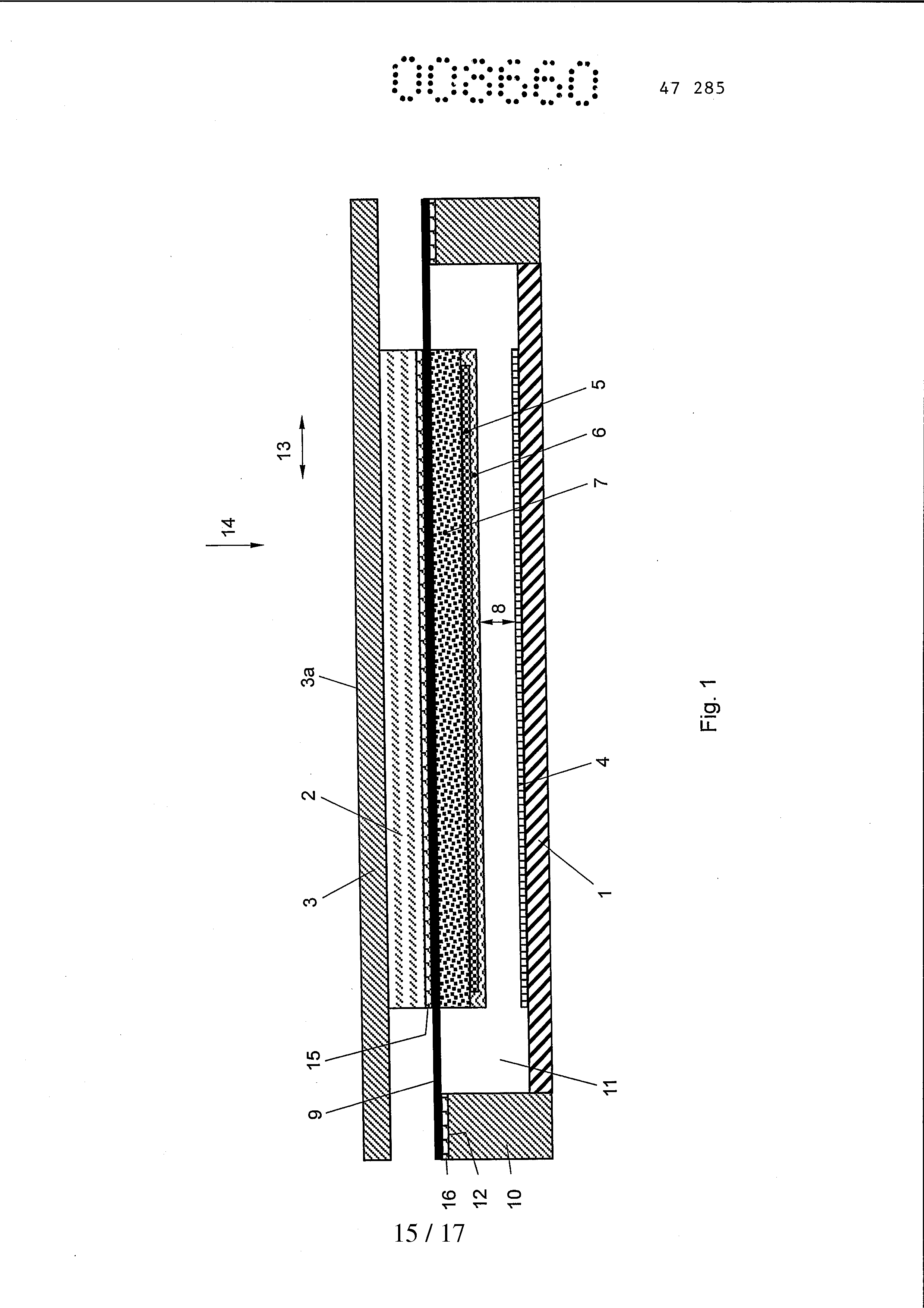
: [...] The invention relates to an actuator for haptic feedback-element of an input element for electronic apparatus is formed as a electrostatic parallel plate-Actuator, comprising in a variable normal spacing between electrode plates held to each other, and between which an electrical voltage can be applied to which a different dielectric is arranged by air. Furthermore, the invention relates to a input member for electronic apparatus, comprising a translationally movable contact surface and haptic feedback-element, deflecting translationally hold the interface, wherein the feedback element has an actuator of the type mentioned above. Such a input member is, for example, described in the WO 2010/080917 Al. The input member, for example, as a touch-sensitive electronic display device (touch screen) is formed. A touch screen is a combined input and output device, in which by contact of parts an image of the program flow of a technical device, usually a computer, can be directly controlled. The input element may also be of a technical equipment a touch pad. This that the contact surface of the touch screen or touch pad is movable in translation., wherein the translational movement is controlled by means of an actuator is created the possibility of a haptic feedback. The control of the actuator as a function of user input can here be carried out, for example, in order to confirm a user input. Such a haptic feedback facilitates the operation of a technical device by means of touch screen or touch pad. The actuator for driving the translational movement of the contact surface is described in the WO 2010/080917 Al in the execution as electrostatic parallel plate-Actuator formed. A electrostatic parallel plate-actuator comprising two electrode plates, are held in a variable normal spacing between each other. The an electrode plate is rigidly arranged relative to a housing or the like of the electronic device. The other, with the contact surface against the force of a return element is deflectable cooperating electrode plate. Between the two electrode plates is provided a gap, in which a dielectric is arranged. If a voltage to the electrode plates is applied now, arise electrostatic forces, which act in the sense of a repulsion or attraction of the electrode plates and a corresponding deflection of the supported to be movable electrode plate effect. The restoring element shall ensure the resetting of the movably supported electrode plate into their starting position. When pressure is applied to the haptic feedback-element is essential an air gap between the electrode plates decreases, whereby the total capacity of the capacitor formed by the electrode plates increases. A high-voltage pulse applied Upon reaching a set point is adjustable, which generates a force impulse, the voltage amplitude is dependent on, inter alia, from the electrode face and the. As dielectric can in a simple way conventional circuit substrates, in particular printed circuit boards from FR -4, are used. In circuit substrates Notes the strength of the force effect of the use of such externally controllable parameters from pulse-to-pulse currently clearly seeing if no change. Again only after a relaxation time of many hours can force strength The original be observed. "Bad" The easiest way of deriving of surface charge offers a dielectric, which, on the one hand, has a sufficiently high conductivity, derive from the air supplied to the charge carrier, on the other hand but a single such small conductivity that exist only in the air on the surface of the dielectric dark dischargesunloading cores be effectively prevented and hot. The latter would be at least-as relevant to the life of the dielectric partial discharge within a dielectric. It flows permanently through the dielectric a withdrawal stream, as soon as a field strength in the dielectric acts and charges are supplied from the air. The conductivity of the dielectric layer opposite a perfect insulating brings with it a further improvement: In increasing the conductivity is, just like the field strength in the dielectric by a higher permittivity increases and thus the effective field strength in the air gap decreases, whereby a greater attractive force possible is tactilely. Conventional circuit substrates high relative permittivity insulation resistances have usually high. Materials with a low relative permittivity also usually have poor insulation resistance. The is thinner the dielectric, the higher is the electric field. Care should be taken to is that the are no disruptive discharges in the material. The ideal dielectric for a good tactile feedback is to have a high relative permittivity of creating a high electric field. It introduces usually a charging of the dielectric, so it is important that the insulation resistance is relatively small, charging (0,1s-ls) derive again in a short time. Is the resistor too large, and the tactile feedback is a charging of the dielectric is carried out with weaker each initiation. Resistance be too small, however, important, to provide a direct conduction and to prevent flashovers. The invention therefore aims, on the label as from, to improve an actuator of the type mentioned that the force impulse generated by the electric field remains strong over a plurality of successive triggerings approximately equal, without the risk of arcing is made. It also limits the overall height of the actuator are minimized. To solve this problem is the actuator of the aforementioned type according to the invention substantially refined in such a way that a relative permittivity of the dielectric 10 1010 Another Optimization according to a preferred improvement thereby succeed that the dielectric a relative permittivity of 20-1000, preferably 50-1000 has. Regarding the insulating resistance can be provided preferably,7- 10 109 a specific insulation resistance of the dielectric that Qm, preferably7-8 Qm has 10 10. What the mechanical structure of the actuator is concerned, provides for a preferred training before that at least one electrode plate relative to a rigidly arranged electrode plates is held deflectable. This may be installed in an input member of an electronic apparatus so the actuator that the movement of the deflectable of the input member is coupled with a contact or The user interface held electrode plate, so that the deflection of the electrode plate leads to a corresponding translational movement of the contact or user interface. If the input member comprises a touch screen, the touch-sensitive surface of the touch screen can form the contact surface of the input element. The deflectable, for example, on the underside of the touch screens arranged electrode plate is held. In order to effect resetting automatically of the actuator, as soon as the voltage pulse applied to the electrode plates is over is preferably provided that the at least one electrode plate can be deflected against the force of a return element. The restoring element can, for example, be constructed as a spring element. An air gap between the two electrode plates is provided in the initial state of the actuator, which allows the movement of the deflectable in the direction of the other electrode plate held electrode plate. The dielectric is preferably on one of the two electrode plates arranged, in particular connected thereto. A preferred embodiment provides that an electrode plate, in particular the rigid electrode plate is formed from a metal plate or a metal mesh. Another preferred embodiment provides that an electrode plate, in particular the at least one deflectable electrode plate, from a metal, in particular copper coating a carrier plate is formed. The carrier plate activity can be formed from a printed circuit board, the copper coating forms the electrode plate. This can be further reduced the overall height of the actuator. In principle it is not the critical factor, whether the rigid or the deflectable connected to the high voltage source held electrode plate, wherein the other electrode plate is in each case connected to ground potential. Preferably, it is also provided that the is held deflectable high voltage-prominent electrode plate. In order to minimize the overall height of the actuator, can be carried out only the dielectric formed as a coating. In this respect, above provides for training One preferred that the dielectric on a electrode plate at least one, in particular on the metal coating, applied dielectric layer comprises. Dielectric layer can be applied, for example, by means of a doctor blade or by the screen printing process. Therefore, the dielectric readily form very thin is provided with preferably, has a thickness of 200- 300μΐη that the dielectric. A preferred selection of the material of the dielectric can be carried out to the effect that the at least one dielectric layer and/or a layer of a resistance paste isolation paste by a layer a is formed. In particular has been shown that with a combination of a resistor paste isolation paste in a simple way with a a dielectric having the values for the relative permittivity and the specific insulation resistance can manufacturing the invention. As isolation paste in so doing the baseline serves. This is slightly made conductive by Mixer the resistor paste. As RS12112 of ESL [...] are used resistor paste can the paste. Epoxy resin base can be used a paste on isolation paste As, such as the paste [...] 243-S of ESL. To adjust the required value of the relative permittivity in a simple way is preferably provided that the at least one dielectric layer with a [...] material, preferably a ceramic powder, such as calcium copper titanium act is offset. The invention is explained in more detail below with reference to an embodiment illustrated schematically in the drawing. In Fig. 1 shows the construction of an input element with the actuator according to the invention. The input member 1 has a frame member 1 on according to Fig., belongs to a housing of electronic equipment. With 2 is designated a touch-screen, i.e. a combination of an electronic display device, such as a LCD-display, with a touch sensor, so that on the display device by touching of parts of the execution of the program of the technical device can be controlled image displayed. The 2 has a touch screen with a contact surface 3a on the touch screen 2 covering [...] 3, which can be contacted by the finger of a user, so as to control the electronic device. Between the touch screen 2 and the housing plate 1 is disposed an electrostatic parallel plate-Actuator, the two electrode plates 4 and 5 has. The first electrode plate is formed as a grid of intersecting electrically conductive wires 4 and is clamped on the frame 1. The second electrode plate 5 is formed as a metal layer applied on a support plate 7 and via the latter to the touch screen 2 connected to common movement. The second electrode plate 6 carries a dielectric 5. Between the Furthermore, 6 and 8 4 the grid remains an air gap dielectric. Between the touch screen 2 and the second electrode plate 9 arranged an elastic transparent film 5 is, in particular bonded (adhesive layer 15), which projects beyond the touch screen 2 on all sides between the housing member 10 and the outer edge and thereby the 2 arranged peripheral gap 11 bridges the touch-screen. The outer edge of the film 9 is mounted on the housing element 10, in particular stuck to it (adhesive layer 16), and at the surface 12 of the housing member 10, the shape of a frame surrounding the touch screen 2. In the initial position of the feedback element 1 represented in 9 is the film Fig. substantially planar tensioned, so that the film in the film plane positioned 9 the feedback-element, in the direction of the double arrow 13 as well as transversely to the plane of the drawing so that it is held substantially immobile. Due to the arrangement of the film 9 is the feedback element 4 relative to the fixed to the housing 1 but starting from the grid in the direction of the arrow 14 shown in Fig. held deflectable starting position. 4 and 5 are so connected to an electrical voltage supply electrode plates The (not shown), a voltage difference can be established between the two electrode plates that 4.5, whereby electrostatic forces arise, which lead to a mutual attraction of the electrode plates 4.5. Here it is preferred that the second electrode plate 5 with a high voltage source 4 with ground potential [...] and the grid. The 6 as a thin coating on the second electrode plate 5 carried out is dielectric and has preferably a thickness of 200-300 pm on. The dielectric coatingisolation paste with a resistor paste can be, for example, a mixture of a, wherein the mixture comprising a ceramic powder, for example. calcium copper titanium act is offset. The invention relates to an actuator for a haptic feedback element of an input element for electronic devices, the actuator being designed as an electrostatic parallel-plate actuator and comprising electrode plates held at a variable normal distance from one another, to which an electrical voltage can be applied and between which a dielectric that differs from air is arranged. In said actuator, the dielectric has a relative permittivity of 5-1000 and a specific insulation resistance of 107-1010 Ωm. 1. actuator for haptic feedback-element of an input element for electronic apparatus is formed as a electrostatic parallel plate-Actuator, comprising in a variable normal spacing between electrode plates held to each other, and between which an electrical voltage can be applied to which a different dielectric is arranged from air, characterized in that a relative permittivity of the dielectric 10 1010 2. actuator according to claim 1, characterized in that a relative permittivity of the dielectric 20-1000, preferably 50-1000 has. 3. actuator according to claim 1 or 2, characterized in that the dielectric7- 10 109 Qm a specific insulation resistance of, preferably7-8 Qm has 10 10. 4. actuator according to claim 1,2 or 3, characterized in that at least one electrode plate relative to a rigidly arranged electrode plates is held deflectable. 5. actuator according to claim 4, characterized in that the at least one electrode plate can be deflected against the force of a return element. 6. actuator according to one of claims 1 to 5, characterized in that an electrode plate, in particular the rigid electrode plate is formed from a metal plate or a metal mesh. 7. actuator according to one of claims 1 to 6, characterized in that an electrode plate, in particular the at least one deflectable electrode plate, from a metal, in particular copper coating a carrier plate is formed. 8. actuator according to one of claims 1 to 7, characterized in that the dielectric on a electrode plate at least one, in particular on the metal coating, applied dielectric layer comprises. 9. actuator according to claim 8, characterized in that the at least one dielectric layer and/or a layer of a resistance paste isolation paste by a layer a is formed. 10. actuator according to claim 8 or 9, characterized in that the at least one dielectric layer with a [...] material, preferably a ceramic powder, for example. calcium copper titanium act is offset. 11. actuator according to claim 8,9 or 10, characterized in that the dielectric has a thickness of 200- 300μκΐ. 12. actuator according to one of claims 8 to 11, characterized in that the carrier plate is formed from a printed circuit board. 13. input member for electronic apparatus, comprising a translationally movable contact surface and haptic feedback-element, deflecting translationally hold the interface, wherein the feedback element comprises an actuator according to one of claims 1 to 12. Vienna, on 12 December 2014 Declarant by