DIGITAL PHASE/CFREQUENCY COMPARISON CIRCUIT FOR A PHASE BLOCKING CIRCUIT.
The available invention concerns a digital PhaseniFrelo quenz Vergleichsschaltung for a Phasenverriegelungsschaltung.
In well-known PLL circuits the phase comparison circuit produces only Phasensignale, which are proportional to the phase error, and as result of it the desired 5 phase stiffness is relatively slowly reached, if the PLL circuit except footstep ist.
It is task of the available invention to plan a phase comparison circuit which responds on the phase error and to the frequency instability in the unbolted condition, around the reaching of the phase stiffness many more rapidly to make possible than with well-known Phasenvergleichsschaltungen.
This task is solved by the characteristics specified in the characteristic of the first requirement. Favourable further educations are the further requirements too entnehmen.
Remark examples of the invention are more near described now on the basis the design. In the design shows:
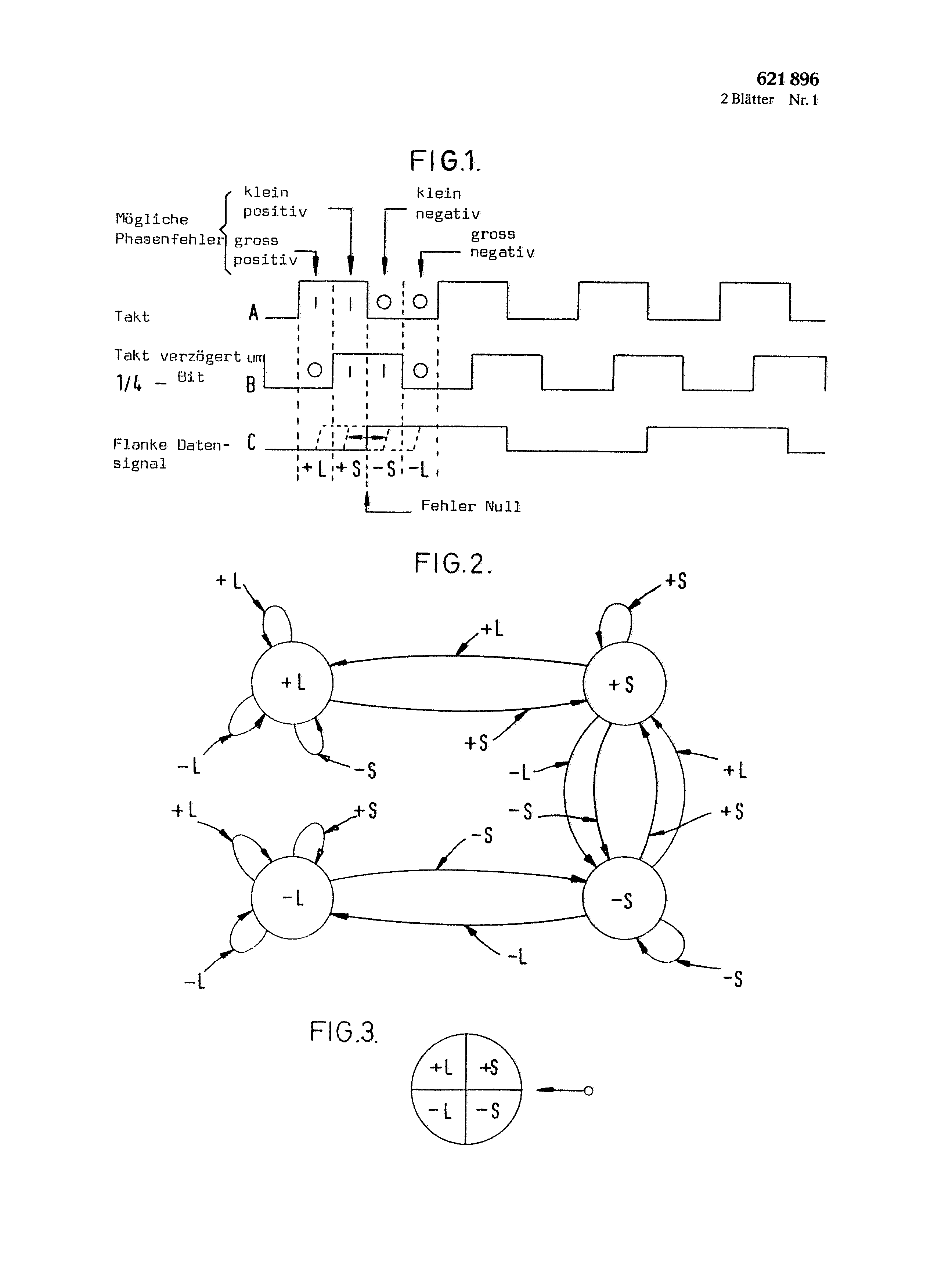
Fig. 1 a Zeitdiagramm for the illustration of the work principle of the phases/frequency Vergleiehsschaltung; Fig. 2 a diagram of the status transition for the phases Frequenza Vergleichsschaltung for a first sentence of rules, as it is indicated in table I; Fig. 3 the phases of the phases/frequency comparison circuit! Fig. 4 a block model of a remark example of the PhaseniFrequenz Vergleichsschaltung; 3s Fig. 5 the status condition for a second sentence of rules, which is indicated in table II; and Fig. 6 a status transition diagram of the phases/frequency comparison circuit for the second sentence of rules gemãss table II.
In accordance with the principles of the available VergleichsschaItung this can be laid out in such a way that she responds both on Frequenzals also to the phase error, as a clock pulse and is scanned a clock pulse with a flank of the data signal, e.g. the rising flank, retarded around V4 - bit period, and these scanning values with that are processed in the following described sequential logic. The 2-Bitcode formed by these scanning values indicates whether the phase error positively (+) or (-) is negative, and whether the phase error largely (L) or (s) is small. If the flank in such a way of the data signal shifts regarding the clock pulse, different 2-Bit-Codesignale results: 10,11, 01 and 00, which are called out + L +S, - S and - L. The sequential logic of the phase comparison circuit has also 2-Bitzustände, which are named likewise + L, + S, - S and - L, in order to manufacture a connection with the phase scanning values. The next condition is shown a function of the preceeding condition and the available scanning value, like this in table I ist.
Table I ahead. Be present. Next condition scanning value condition +L ÷L +L +L +S +S ÷L - S +L +L - L +L +S +L +L Vorausg. Be present. Next condition Abtastwerl condition +S - S - S +S - L - S - S +L +S - S +S +S - S - S - S - S - L - L - L +L - L - L +S - L - L - S - S - L - L - L the rules given in table I are in Fig. 2 figurativy represented. The four circles represent the conditions, the arrows show the changes of the condition and the designations on the arrows represent the phase scanning values, which the condition for the reaching of this status change darstellen.
The positions of the conditions in Fig. 2 is in such a way arranged, around the cyclic consequence in Fig. to point out 3 phases shown, with which the phase error zero between + S and - S liegt.
Phase changes in the clockwise direction result in a negative frequency instability and phase changes Irish Republican Army counter-clockwise direction a positive frequency instability. From the view of table I and Fig. 2 it can be seen that the next condition is in most cases the same as with the available scanning value. Exceptions are marked with one * or with ** in table I. Those with * marked exceptions cause that the condition (+) becomes, if always the frequency instability (+) is (phase rotation the counterclockwise), and (+) remains, so for a long time the frequency instability (+) remains. The condition can return on (-) only if the phase the zero point in the opposite direction, i.e. in the clockwise direction, kreuzt.
A similar, but opposite relationship is valid for negative Frequenzfehler.
Only if the phase is very irregular, because of bad receipt conditions, the phase of the scanning value changes on not neighbouring phase positions, e.g. from + S up - L. with ** exceptions marked in table I result in such cases a minimum change from Null.
The output signal of the phases/frequency comparison circuit indicates whether the condition (+) or (-) is. If a frequency instability is present (PLL is except TritO, indicates the output signal the direction of the frequency instability. If the frequency instability zero is (PLL locked), becomes the phase normally between +S and - S to vary and the output signal gives the direction of the Phasenfehlcrs an.
Without the possibility of frequency detection both s0 becomes (+) - and (-) - phase error detects, if the PLL is fallen except footstep. The loop is only corrected therefore in correct direction, i.e. toward renewed bolting device, because (+) - the phase error is detected a little more frequently than (-) - the phase error, if the frequency instability (+) is. Ähnss more licher, however opposite condition results, if the frequency instability (-) is. The correction strength is much weaker from there than with a constant announcement of (+) or (-), like this by the phases/frequency comparison circuit of the above-mentioned kind the case ist.
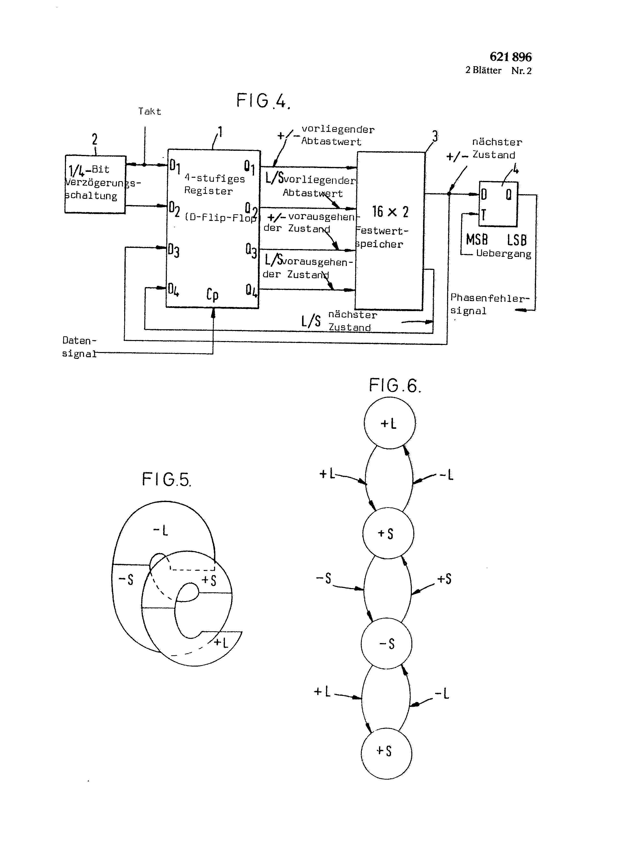
Fig. a block model of a remark example of the phase comparison circuit shows 4. The use of this execution of the phases/frequency comparison circuit in a PLL is represented in the request for US patent No. 702,803. In Fig. 4 the data input signal is attached to the clock input CP of a vieres level register I, whereby the clock pulse is digitally coupled rait the first D-Flip-flop of register I and over a l/4 - bit delay circuit 2 with second 621,896 the D-Flip-flop of register 1. the Q1 - exit of the first flip-flop stage results in a signal, which () - phase error of the available data scanning value indicates. The Qz-output signal of the second stage of register 1 gives a signal, which indicates whether a large or small phase error is present with the available data scanning value. These signals are in accordance with Fig. to 1 coded and 16 x 2-Fcstwertspeicher 3. the memory 3 arrive possess a first exit, at which a signal appears, that are representing for () - the error signal of the next condition of the data at, and a second exit, with a signal, that it is representing for the fact whether the phase error of the next condition of the data will be large or small. These two exits are connected with your course third and/or a fourth D-Flip-flop-stage of register 1, in order to deliver at their exits of signals, those are representing for the conditions of the vorausgegangeñen Daten.
The output signal of the third stage of register 1 is, that is representing a signal for () - the error signal of the preceeding data sample, and the output signal of the fourth stage of register 1 is, that representing a signal is “largely/small” for the error signal the preceding data scanning value. The two signals for the available scanning value, the two signals for the preceeding condition and the two signals for the next condition are actually signals in Fig. 1 represented 2-Bit-Codesignale.
The phase error signal of the comparison circuit is emitted by a D-Flip-flop 4, whose your course is coupled with the /--Phasenfehlersignal of the next condition of the data of the memory 3, whereby the clock input is clocked by the flip-flop 4 by a clock pulse, that the transition of the most important bit MSB i.e. of the last bit of a data item to few most important bits (LSB), i.e. for the first bit of the next data item darstellt.
The read-only memory 3 is wired or coded gemãss table I, in order to result in the desired output signal, which is certain by the four input signals attached to it. Table II Vorausg. Be present. Next condition scanning value condition +L +L +S +L +S +L +L - S +L +L - L +L +S +L +S +S +S +S +S - S - S +S - L +L - S +L - L - S +S +S - S - S - S - S - L - S - L +L - L - L +S - L - L - S - L - L - L - S the above table II shows a second sentence of rules, like it in the Vergleichssehaltung after Fig. 4 to be used can. The phases existing with this sentence of rules are the same, as in Fig. 3, while the conditions in Fig.
are shown. Fig. the status transition diagram of table II shows 6, whereby the circles, arrows and the addresses connected with the arrows have the same meaning as in Fig. 2.
The only difference of the circuit after Fig. it consists 4 for table II of the fact that the read-only memory codes 3 instead of according to table I, according to table II or wires ist.
G 2 sheets designs of 621,896 2 pages No. 1 FI6.1.
Phases feh lerI largely L positively clock A -- Clock VE zößert u 1 II. - Bit B I small flank data signal…. I i I poured negatively “, Ioi°1, I negatively! I! I J! ! I o, 1°: , I I I 1 I ....... I; _.t,” “I I,” I l.J': - '“ç I! ! I t ù+ L, +S”, - S, - L, I 1 error zero I I-- FIG.2.
+L +S - L - S +L - L +L +S FIG.3.
ùI---o Two D-type flip flops have a clock and a 1/4-bit delayed clock coupled to the D inputs of respective ones of the two flip flops to provide a +/- phase error of a present sample of digital data coupled to the clock inputs of the two flip flops and a second signal indicating a large/small phase error of the present sample of the data. A third signal indicating a +/- phase error of a previous state of the data is provided and a fourth signal indicating a large/small error of the previous state of the data is provided. A read only memory is responsive to the first, second, third and fourth signals in accordance with a given set of rules to produce a phase error signal with a clockwise change of phase states of the data providing a negative frequency error signal and a counter-clockwise change of phase states of the data providing a positive frequency error signal. 1. A digital phase/frequency comparator comprising: a first source of clock; a second source of digital data; first means coupled to said first and second sources to produce a first signal indicating a plus/minus phase error of a present sample of said data and a second signal indicating a large/small phase error of said present sample of said data; second means to provide a third signal indicating a plus/minus phase error of a previous state of said data and a fourth signal indicating a large/small phase error of said previous state of said data; and third means coupled to said first and second means responsive to said first, second, third and fourth signals following a given set of rules determined by a predetermined logic to produce a phase error signal, said first, second and third means cooperating to provide negative frequency errors for a clockwise change of phase states of said data and positive frequency errors for counter-clockwise changes of phase states of said data. 2. A comparator according to claim 1, wherein said third means includes a read only memory wired according to said set of rules coupled to said first and second means responsive to said first, second, third and fourth signals, said memory having a first output providing thereon a first output signal in accordance with said set of rules indicating a plus/minus phase error of a next state of said data and a second output providing thereon a second output signal in accordance with said set of rules indicating a large/small phase error of said next state of said data, and a D-type flip flop coupled to said first output responsive to said first output signal and most significant bit to least significant bit transition timing signals to produce said phase error signal. 3. A comparator according to claim 2, wherein said first means includes a delay circuit having a 1/4-bit delay coupled to said first source to delay said clock 1/4-bit, and one pair of stages of a four stage register having its clock input coupled to said second source, one of said one pair of stages being coupled to said first source to produce said first signal for coupling to said memory and the other of said one pair of stages being coupled to said delay circuit to produce said second signal for coupling to said memory. 4. A comparator according to claim 3, wherein said second means includes the other pair of stages of said register, one of said other pair of stages being coupled to said first output of said memory to produce said third signal for coupling to said memory and the other of said other pair of stages being coupled to said second output of said memory to produce said fourth signal for coupling to said memory. 5. A comparator according to claim 4, wherein each of said stages of said register is a D-type flip flop. 6. A comparator according to claim 1, wherein said first means includes a delay circuit having a 1/4-bit delay coupled to said first source to delay said clock 1/4-bit, and one pair of stages of a four stage register having its clock input coupled to said second source, one of said one pair of stages being coupled to said first source to produce said first signal for coupling to said memory and the other of said one pair of stages being coupled to said delay circuit to produce said second signal for coupling to said memory. 7. A comparator according to claim 5, wherein said third means further produces a fifth signal in accordance with said set of rules indicating a plus/minus phase error of a next state of said data and a sixth signal in accordance with said set of rules indicating a large/small phase error of said next state of said data, and said second means includes the other pair of stages of said register, one of said other pair of stages being coupled to said third means to store said fifth signal to produce said third signal for coupling to said third means and the other of said other pair of stages being coupled to said third means to store said sixth signal to produce said fourth signal for coupling to said third means. 8. A comparator according to claim 7, wherein each of said stages of said register is a D-type flip flop. 9. A comparator according to claim 1, wherein said third means further produces a fifth signal in accordance with said set of rules indicating a plus/minus phase error of a next state of said data and a sixth signal in accordance with said set of rules indicating a large/small phase error of said next state of said data, and said second means includes a pair of flip flops, each having their clock input coupled to said second source, one of said pair of flip flops being coupled to said third means to store said fifth signal to produce said third signal for coupling to said third means and the other of said pair of flip flops being coupled to said third means to store said sixth signal to produce said fourth signal for coupling to said third means. 10. A comparator according to claim 9, wherein each of said flip flops is a D-type flip flop.