LED, for displays and communications, is based on amorphous p-type, n-type and p-n-type aluminum-indium-gallium nitride semiconductor layers
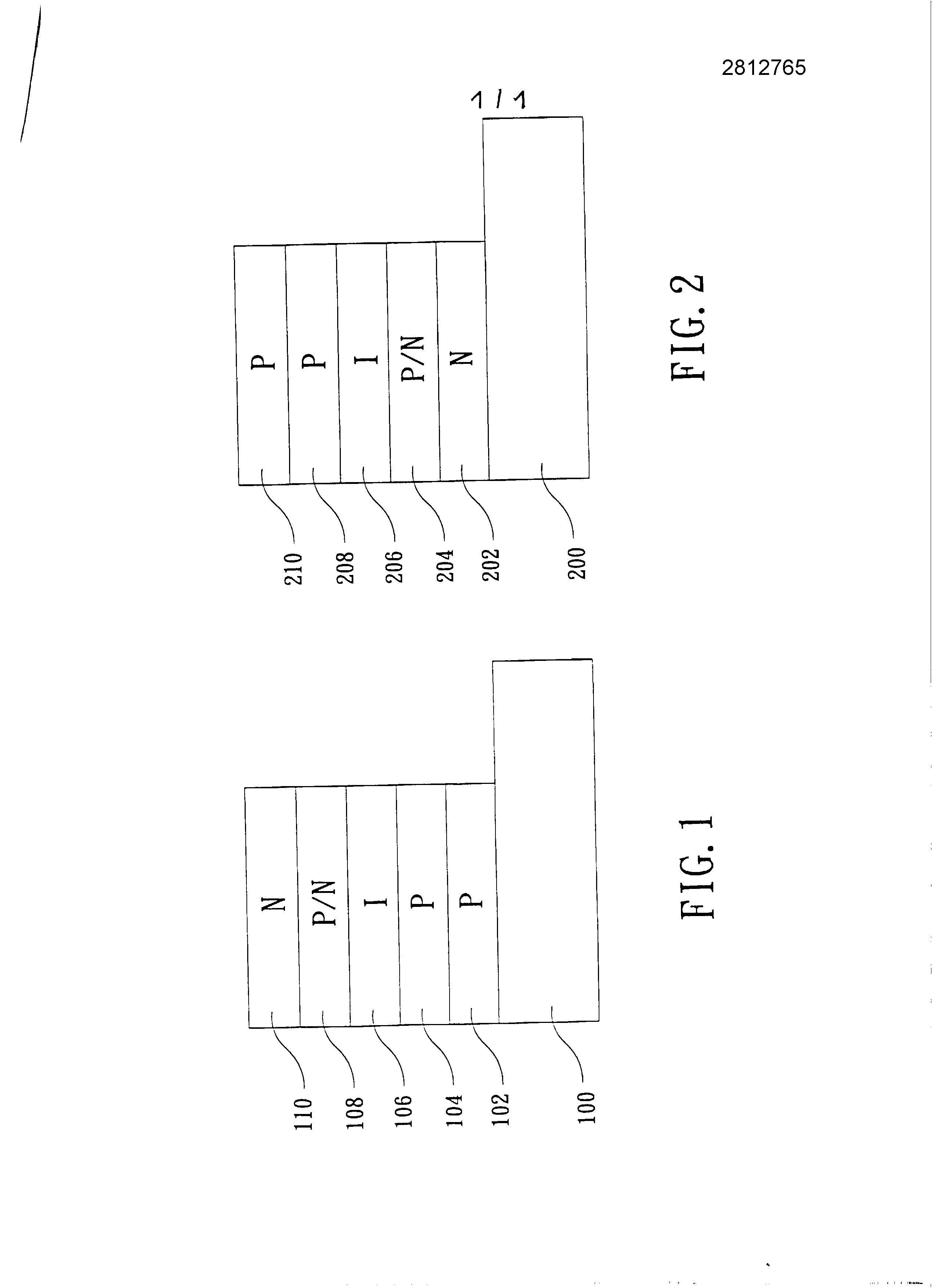
Field of the invention The present invention comprises a light emitting diode in amorphous AlInGaN, particularly to a light emitting diode in AlInGaN amorphous low manufacturing cost and high yield. The compound semiconductor devices have been usefully applied to the products display and communication, andc. More particularly, the compound semiconductor of GaN retained 11 have much attention due to their ability to emit blue light. The-based compound semiconductor of GaN is bandgap materials directly with a power transfer rate highly efficient and has a wide energy distribution, 2.0 eV to 6.4. Patent US The No. 5,563 422 has provided a method for manufacturing compound semiconductors GaN-based, wherein compound semiconductors GaN-based crystal are specifically used to make the light emitting diodes. However, the compound semiconductor crystalline GaN have the problems of high cost and low efficiency. Therefore, it is the object of the present invention to provide a light emitting diode in amorphous AlInGaN with low manufacturing cost and high efficiency. To achieve the above objective, the present invention provides a light emitting diode in amorphous AlInGaN comprising, in order, a substrate p-type GaN, a first semiconductor layer of a compound-type amorphous p, a second semiconductor layer of a compound-type amorphous p, a semiconductor layer of a compound doped amorphous ("an amorphous [...] compound semiconductor layer"), a semiconductor layer of a compound-type amorphous p/n and a semiconductor layer of a compound n-type amorphous. Furthermore, for achieving the above object, ' the present invention provides a light emitting diode in amorphous AlInGaN comprising, in order, a sapphire substrate, a semiconductor layer of a compound n-type amorphous, a semiconductor layer of a compound-type amorphous p/n, a semiconductor layer of a compound doped amorphous, a second semiconductor layer of a compound-type amorphous p and a first semiconductor layer of a compound-type amorphous p. The various objects and advantages of the present invention will be understood more readily from the following detailed description when read together with the accompanying drawings, on which: Figure 1 is a cross-sectional view of the light emitting diode into amorphous AlInGaN according to the first preferred embodiment of the present invention; figure 2 is a cross-sectional view of the light emitting diode into amorphous AlInGaN according to the second preferred embodiment of the present invention. Maintaining With reference to Figure 1, the present invention is intended to provide a light emitting diode in amorphous AlInGaN with low manufacturing cost and high efficiency. In amorphous AlInGaN The light emitting diode according to the present invention comprises, in the order, ' a p-type GaN substrate 100, a first semiconductor layer of a compound-type amorphous p 102, a second semiconductor layer of a compound-type amorphous p 104, a semiconductor layer of a compound doped amorphous 106, a semiconductor layer of a compound-type amorphous p/n 108 and a semiconductor layer of a compound-type amorphous n 110, wherein the layers 102 to 110 can be formed by vapor phase growing. The first semiconductor layer of a compound-type amorphous p 102 acts as a buffer layer. The second semiconductor layer of a compound-type amorphous p 104 acts as upper confinement layer. The layer of compound semiconductor doped amorphous 106 has a low resistance to act as light-emitting layer. The semiconductor layer of a compound-type amorphous p/n 108 acts as upper confinement layer. The semiconductor layer of a compound-type amorphous n 110 acts as electrode and forms a junction p/n. It should be appreciated that the layers have, in cross section, a rectangular shape, including a square shape. Furthermore, Bollards the light emitting diodes are formed in two recesses (" [...] teeth") etched (not shown) on the semiconductor layer of a compound-type amorphous n 110, while the single pad the light emitting diode in U.S. Patent No. 5,563 422 is formed in a single trough etched. The p-type impurity is selected from the group consisting of zinc, magnesium, beryllium, strontium, barium and cadmium and has an impurity concentration of 1014'22 EA/ cm3. The n-type impurity is selected from the group consisting of silicon, germanium, tin, sulfur, selenium and tellurium and has an impurity concentration of 10 ~ The reaction gas contains ammonia or 1 'hydrazine, or trimethyl aluminum combined with ammonia and 1' hydrazine and the reaction gas can, further, contain the gas from the single or combined trimethyl-gallium and/or triethylgallium. Furthermore, the reaction gas contains, further, at least one gas of diethyl-zinc, trimethyl-zinc, trimethyl indium and [...]. Figure 2 is a cross-sectional view of the light emitting diode into amorphous AlInGaN according to the second preferred embodiment of the present invention. The present invention provides a light emitting diode in amorphous AlInGaN comprising, in order, a sapphire substrate 200, a semiconductor layer of a compound-type amorphous n 202, a semiconductor layer of a compound-type amorphous p/n 204, a semiconductor layer of a compound doped amorphous 206, a second semiconductor layer of a compound-type amorphous p 208 and a first semiconductor layer of a compound-type amorphous p 210, wherein the layers 202 to 210 may be formed by vapor phase growing. The semiconductor layer of a compound-type amorphous n 2,02 acts as a buffer layer. The semiconductor layer of a compound-type amorphous p/n 2,04 acts as upper confinement layer. The layer of compound semiconductor doped amorphous 206 has a low resistance to act as light-emitting layer. The second semiconductor layer of a compound-type amorphous p 208 acts as upper confinement layer. The first semiconductor layer of a compound-type amorphous p 210 acts as electrode and forms a junction p/n. It should be appreciated that the layers have, in cross section, a rectangular shape, including a square shape. Furthermore, Bollards the light emitting diodes are formed in two recesses etched (not shown) on the first compound semiconductor layer-type amorphous p 210, while the single pad the light emitting diode in U.S. Patent No. 5,563 422 is formed in a pit etched. The p-type impurity is selected from the group consisting of zinc, magnesium, beryllium, strontium, barium and cadmium and has an impurity concentration of 10 * The reaction gas contains ammonia or 1 'hydrazine, or trimethyl aluminum combined with ammonia and 1' hydrazine and the reaction gas can, further, contain the gas from the single or combined trimethyl-gallium and/or triethylgallium. Furthermore, the reaction gas contains, further, at least one gas of diethyl-zinc, trimethyl-zinc, trimethyl indium and [...]. While the present invention has been described with reference to its preferred embodiment, it will be understood that the invention is not limited to the details thereof. Various substitutions and modifications have been suggested in the above description, and other will have is to those skilled in the art. Therefore, all such substitutions and modifications are intended to be included in the scope of the invention as defined in the attached claims. The LED is based on amorphous p-, n- and p/n-type aluminum-indium-gallium nitride (AlInGaN) semiconductor layers. The amorphous AlInGaN LED comprises a p-GaN substrate (100) bearing a sequence of a first amorphous p-type compound semiconductor layer (102), a second amorphous p-type compound semiconductor layer (104), an amorphous compound semiconductor impurity layer (106), an amorphous p/n-type compound semiconductor layer (108) and an amorphous n-type compound semiconductor layer (110). An Independent claim is also included for an amorphous AlInGaN LED comprising a sapphire substrate bearing a sequence of an amorphous n-type compound semiconductor layer, an amorphous p/n-type compound semiconductor layer, an amorphous compound semiconductor impurity layer, a second amorphous p-type compound semiconductor layer and a first amorphous p-type compound semiconductor layer. 1. Amorphous AlInGaN light emitting diode characterized in that it comprises, in order, a substrate-type GaN p (100), a first semiconductor layer of a compound-type amorphous p (102), a second semiconductor layer of a compound-type amorphous p (104), a semiconductor layer of a compound doped amorphous (106), a semiconductor layer of a compound-type amorphous p/n (108) and a semiconductor layer of a compound n-type amorphous (110). 2. Amorphous AlInGaN light emitting diode according to claim 1, characterized in that the impurity is selected from the group consisting of zinc, magnesium, beryllium, strontium, barium and cadmium and has an impurity concentration of 1014 '22 EA/Cm3 . 3. Amorphous AlInGaN light emitting diode according to claim 1, characterized in that the n-type impurity is selected from the group consisting of silicon, germanium, tin, sulfur, selenium and tellurium and has an impurity concentration of 1014 ~22 EA/Cm3 . 4. Amorphous AlInGaN light emitting diode according to claim 1, characterized in that the reaction gas contains ammonia or 1 'hydrazine, or trimethyl aluminum combined with ammonia and 1' hydrazine and the reaction gas can, further, contain the gas from the single or combined trimethyl-gallium and/or triethyl gallium. 5. Amorphous AlInGaN light emitting diode according to claim 4, characterized in that the reaction gas contains, further, at least one gas of diethyl-zinc, trimethyl-zinc, trimethyl indium and cyclopentadienyl-magnesium. 6. Amorphous AlInGaN light emitting diode, characterized in that it comprises, in order, a sapphire substrate (200), a semiconductor layer of a compound n-type amorphous (202), a semiconductor layer of a compound-type amorphous p/n (204), a semiconductor layer of a compound doped amorphous (206), a second semiconductor layer of a compound-type amorphous p (208) and a first semiconductor layer of a compound-type amorphous p (210). 7. Amorphous AlInGaN light emitting diode according to claim 6, characterized in that the impurity is selected from the group consisting of zinc, magnesium, beryllium, strontium, barium and cadmium and has an impurity concentration of 1014 '22 EA/Cm3 . 8. Amorphous AlInGaN light emitting diode according to claim 6, characterized in that the n-type impurity is selected from the group consisting of silicon, germanium, tin, sulfur, selenium and tellurium and has an impurity concentration of 1014 '22 EA/Cm3 . 9. Amorphous AlInGaN light emitting diode according to claim 6, characterized in that the reaction gas contains ammonia or 1 'hydrazine, or trimethyl aluminum combined with ammonia and 1' hydrazine and the reaction gas can, further, contain the gas from the single or combined trimethyl-gallium and/or triethyl gallium. 10. Amorphous AlInGaN light emitting diode according to claim 9, characterized in that the reaction gas contains, further, at least one gas of diethyl-zinc, trimethyl-zinc, trimethyl indium and cyclopentadienyl-magnesium. DIODE [...] EN AlInGaN [...]
Context of the invention
Breve description of the drawings
Detailed description of the preferred embodiment