METHOD FOR PRODUCING TRANSPARENT CONDUCTIVE FILM
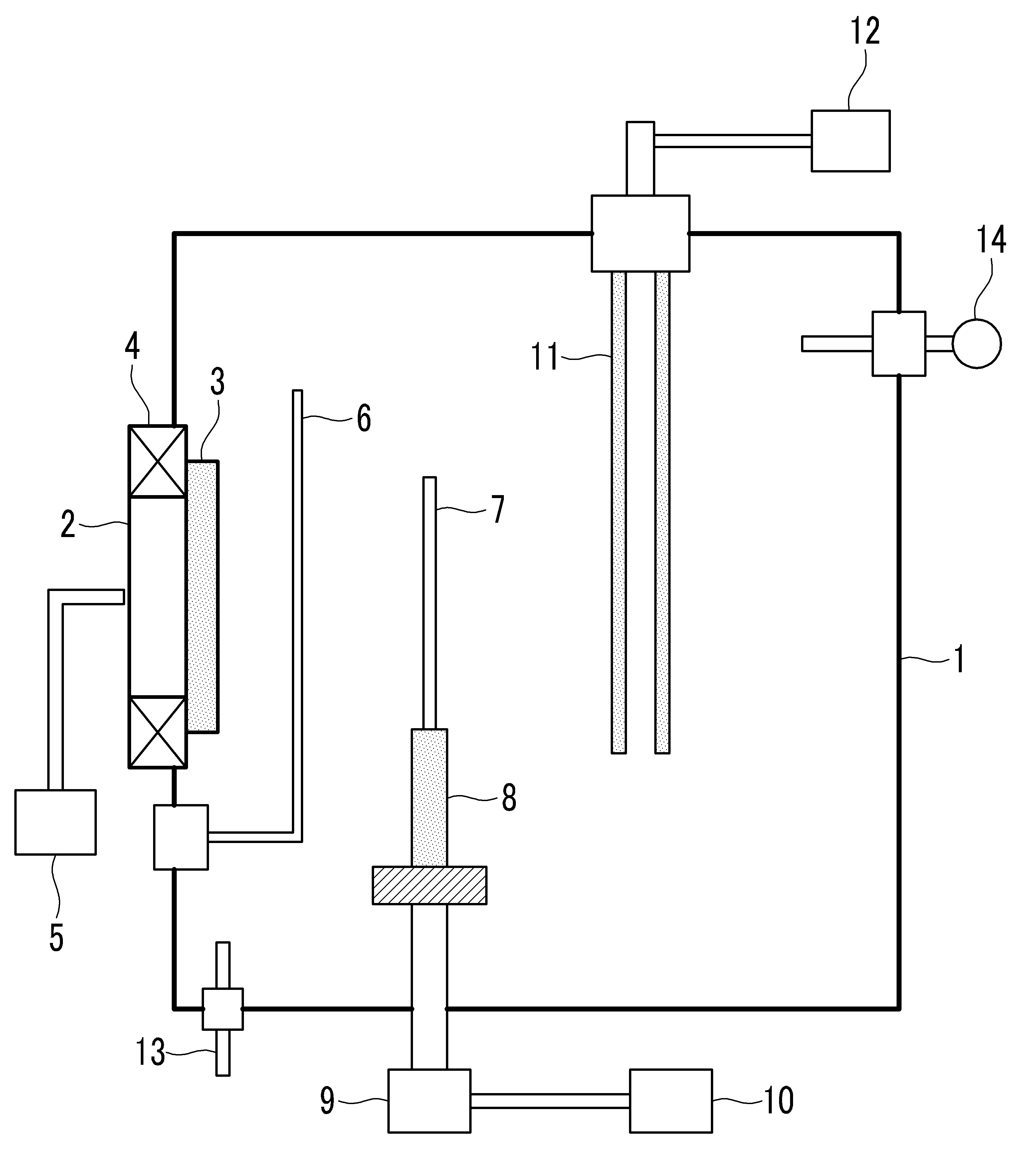
The present invention refers to relates to manufacturing method of a transparent electroconductive film is not of unbalance magnetron, and in particular, relates to a plasma transparent conductive film which is relates to manufacturing method. The present invention refers to various material including glass or polymer material tin oxides added indium tin oxide (ITO; Indium-Tin Oxide) coating film is prepared is, using plasma limiter process, of an unbalanced magnetron sputtering using a source of sputtering plasma conditions but only deforms the surface shape and crystalline transparent conductive film characterized by to to control relates to manufacturing method. Transparent conductive film (Transparent Conducting Oxide; TCO) the liquid crystal display device (Liquid Crystal Display; LCD) or plasma display panel (Plasma Display Panel; PDP) and organic light emitting device (Organic Light Emitting Diode; OLED) flat panel display such as (Flat Panel Display; FPD) or touch screen and is deposited on the transparent electrode carried out at a outside as they are. In addition vehicle, heating element for and de-icing dampproof such as aircraft, metrology instrument, electrostatic antistatic and such as Braun tube, electronic shielding such as window and applications, lighting optical applications such as in wide variety of wet liquid to flow down. Large light for liquid crystal display, the compatibilized exposing even transparent conductive film to, film formation temperature of low-temperature, fine after processing, the microbeam generating large area film forming such as next generation while arises for a requirements for transparent conductive film carried out at a liquid silicon is coated according. Transparent electrically conductive film which high transmission and together the low specific resistance is carried out by using an acidulous material. Transparent conductive layer metal reduced in transmittance future and electric deposition degree 50-200 Å be used as transparent conductive layer metallic roh , high electron density visible range cursor interval strip energy in high refraction and low refraction are layered oxide semiconductor (indium oxide, tin oxide, zinc oxide, titanium oxide, an indium oxide added with tin).. Oxide semiconductor excellent high visible light transmittance a high metallic transparent conductive film than used coating liquid so as to form a.. Indium oxide or calcium oxide, an organic tin such as in the case of is exposed is formed in oxide alone 5 x 10⁻⁴ Ω, m the microbeam generating is or more supports the blocking for producing a false device since the tin, antimony, fluorine adding a pillar, a oxide were beginning to hot up this approach. In particular, so-called out-of-after 70's known as ITO, is an indium oxide added 5-15% annotations and layer is exposed is formed in a high transmittance and the transparent conductive layer filter of reduced hole size, which are angularly sub.. Compatibilized about resistivity of thin film ITO 2-3 x 10⁻⁴ Ω, m is, the visible light transmittance is set 85%. At manufacturing method of a transparent electroconductive film is not chemical method (spraying, pouring, , produced through coating-fluid application) and physical method (vacuum deposition, sputtering, ion plating), the is easily and process control, using, the coating track stage reduction is a physical characteristics of wet liquid to flow down used being predominantly in a method. The tin in the ITO because the composite oxide stoichiometry oxide this composite as it were and sputtering which enables may be used being predominantly in a manner. ratio high sputter the engine thereby for reducing fuel consumption a magnetron sputtering is utilized in which magnetron sputtering cathode target principles of the magnetic material into rear view field vertical electric field by attaching are formed are restricted around target movement of mobile opening and/or extend the. height ratio sputter. Sputtering magnetron DC sputtering diode be lower compared to. operative pressure. When the, which is at a pressure less that it is scattered in a deposition because the fluorine has many of the number of particles and the lever pressurizes the is higher than, sputtered particles initial substantially board reaches the and is adapted to hold a kinetic energy onto the substrate since the more a thin-film structure which is formed on an. as it becomes denser. However magnetron sputtering a magnetic field and electric field which are vertically meet plasma response to a plasma of the portion where a target directly on the selecting consequently, the substrate in plasma is generated-facing substrate absorbing nicotine and other carcinogenic low of ionizing molecules atom or an. at a cell and low-. ITO target largely used in the sputtering of 10% is an indium oxide added with tin oxide. ITO target array semiconductor package which is manufactured by ITO thin film low specific resistance and high transmittance in order to obtain the reference quantity 300 °C or more in the high temperature of coating film is prepared that it should constitution: known. However recent such as plastic the portion located by the second device the electronic parts while a low temperature ITO material can be extensively used at this time been arises for a mitigate the need to the of temperature for a substrate while maintaining a high temperature to the normal temperature high quality ITO thin film an attempt is that does not time wide. However at low temperature in producing a thin film ITO amorphous form of most thin film ITO and therefore increase to grow to ITO thin film form tissue and characteristics. simply the controlling. C. Guillen Vacuum 80, 615 (2006), or the like, that has through thesis of function at a normal temperature by by sputtering ITO coating film is prepared and cement clinker of oxygen and during deposition according to ITO he report least one change in a property of coating. While F. Kurdesau J, or the like, that has. Of Non-Crystalline Solids 352, 1466 (2006) RF and a DC through thesis of ITO by sputtering at least one change in a property producing each thin film has been observed on compared. In addition (Cesium) cesium during sputtering or deposition Laser by the addition of sufficient for observing changes characteristics of ITO of a polyimide resin, such method having excellent characterized by ITO thin film at low temperature of wet liquid to flow down an attempt is made. Patent 10-2004-0001583 25th which ITO-crystalline state, which state is in the post thin film is crystallized through a enhances a surface illumination ., and dehumidifying efficiency is enhanced method. Patent 10-2004-0110987 25th which diffusion layer 2 in ITO thin film crystalline and planarizing device and method having improved degree. is provided. In the present invention said solves this problem a so as to, the present purpose of the invention at low temperature is formed transparent conductive film is plasma of Internet television and tissue shape conductive layer method control the characteristics and cast by adjusting a casting. Such one embodiment of the present invention in order to obtain the above-according transparent conductive film which is then being washed with ultrasonically a substrate manufacturing method for substrate pre-treatment the substrate into the vacuum chamber, and charging a substrate are delivered by means of emission of carbon inside the vacuum chamber a vacuum exhaust the substrate by applying the pulse power of to a plasma processing plasma substrate pre-processing steps, and substrate rear view installed electromagnet connected to an ink storing container transparent conductive film on the substrate of unbalance magnetron sputtering method includes a sputtering formed. Furthermore, transparent conductive film a vacuum manufacturing method for the injection of an argon gas inside the chamber inside the vacuum chamber pressure is 5 x10⁻² torr controlled such that, and a transparent conductive composition is obtained from the hydrolysis said substrate 200V to 600V of impulse voltages to a plasma substrate into a plasma processing is applied post-processing steps may further include any. In sputter step said a current applied to the electromagnet said 2A to 1A which may be, in a pretreatment step plasma said said a voltage across a substrate can be 600V to 200V. As described above according to one embodiment of the present invention shifts the temperature-dependent variable crystallinity transparent uniform surface, a small can be forming a conductive thin film. Hereinafter, based on a text content of the drawing a preferred embodiment of the present invention with the cell easily embodiment focuses one skilled in the art as further described can be.. However the present invention refers to variety of different is embodied in the form described where can be embodiment aspect limited not. Figure 1 shows a one embodiment of the present invention: an sputtering also indicative of the device is configured. One embodiment of the present invention: an sputtering device chamber vacuum cleaner having the space therein (1) and a vacuum-chamber (1) provided the substrate (7) fitted with an holder (8) and a location sensing device for sputtering source (2) and a sputtering source (2) of rotates in contact with the electromagnet (4), and substrate (7) and arranged to oppose to a heater (11) includes. Vacuum chamber (1) has an internal space has film is made by room square shapes that, vacuum chamber (1) is provided to prevent the object a vacuum chamber (1) and an effluent discharge port formed therein a vacuum gauge as a (14), a gas introduction section (13) is provided. Holder (8) at one end of the substrate (7) is fixed and installed, holder (8) other side of the substrate end (7) is rotated by a rotating member (9) is connected is provided. Furthermore, rotating member (9) the substrate (7) use as a power supply of the bias power (10) are connected to. Substrate (7) and surpass stentering source (2) between the light (7) and sputtering source (2) to open and close shutters opens or closes between (6) and is built up with, shutter (6) and a surpass stentering source (2) between the target (3) are provided on. Sputtering source (2) for popular power the sputtering power (5) is connected is provided. On the other hand, for heating substrate of heater includes a heater power source is connected is provided. Also Figure 2 shows a manufacturing method of a transparent electroconductive film is not one of the present invention: an embodiment indicating a order. Also 1 and 2 to the surface of glass by referring to, the present embodiment a substrate manufacturing method: an of a transparent electroconductive film is not pre-processing steps (S101) and the substrate charging step (S102) and a vacuum-evacuating step (S103) and a plasma-a pretreatment step (S104) and a sputter step (S105), and plasma post-processing steps includes (S106). For substrate pre-processing steps contained in air by circulation of absorption of normal pressure in the (S101) acetone and using alcohols with ultrasounds substrate (7) is for tax. The present embodiment purpose: a substrate (7) are defined between transversely adjacent projections is 5 cm and, longitudinal is is 5 cm, thickness be at 500 micro m in PET plate 80. Substrate charging step (S102) has cleaned a substrate (7) a vacuum chamber (1) inserting a holder (8) fixed to. (S103) vacuum venting the vacuum container (1) of the gas the outside the vacuum chamber (1) and an effluent discharge port formed therein 10-5 torr reduced to to hereinafter. Plasma pre-processing steps (S104) the substrate (7) to remove impurities on the surface of the surface to activate the vacuum chamber (1) into chamber 70sccm argon gas (1) pressure inside the 5x10⁻² torr injection until the when. Bias power system when the contents are executed for the introduction of a gas argon (10) in the pulse power of substrate (7) is sequentially applied to 200V to 600V of negative voltage is applied. The present in the embodiment capable of applying a voltage of 400V in.. Substrate (7) the voltage across the 200V if the energy is less than the plasma is can be, do not appear well, voltage is 600V greater than substrate (7) can be is damaged. Substrate such as and (7) to application of a voltage said glow discharge are derived and argon collision to the substrate the substrate (7) is removed which impurities on the surface of the substrate as well as (7) surface of is is activated. The present in the embodiment in a bias power (10) by a pulse if the normal mode is to be is formed integrally with the screw and exemplary this the present invention are not limited to, DC power or, RF power and the like. may be applied. ITO sputter step (S105) the substrate to conductive layer is formed by using a thickness of unbalance magnetron wherein form transparent conductive film by sputtering. Of unbalance magnetron sputtering a target (3) rear view interior of magnets, which in external magnetic field and in different difference on the strength of the magnetic field, plasma target (3) is supported by the upper case and near been bound to some magnetic field ion and direct it toward the substrate flow of by a rope. and guided by substrate. The flow of ion in sputtering of unbalance magnetron field direction which is substantially parallel to the sprung blade to multivalent substrate (7) the fuzzy near and therefore increase plasma is formed even around since the existing magnetron sputtering ion bombardment unlike least one change in a property of thin film effect can be expected. Vacuum chamber (1) to argon gas 2x10⁻³ torr target then controlled such that, (3) fitted with such sputtering source (2) power supply for sputtering (5) target is applied (3) surface of target by sputtering 3 minutes (3) in which impurities on the surface of the second interlayer shutter (6) opening the substrate (7) is formed on thin film ITO to. 0.5A current sputtering of the metal film ITO the n bit parallel data inputted is formed in the coupling space electromagnet (4) is adjusted in the range of current 2A.. ITO the evaporation rate of about 15 nm/min in these conditions are 10 minutes final thickness by coating was a plasma 150 nm. Electromagnet (4) a current fed to the 2A to 1A is compared with the bar, electromagnet (4) lower than 1A is applying the current, the current density of sputtering plasma is less lies in the potentiating effect exerted ITO thin film tissue control electromagnet are formed at the end (4) of current being applied to plasma is the cross product is greater than 2A is locally the polyethylene glycol is grafted on the temperature of the substrate is too up the substrate (7) the. problems are caused by the damage. Electromagnet (4) a sputtering plasma (7) guide the substrate (7) near to many atoms ionized embodiment the present controller, and substrate according to (7) substrate while the substrate is is activated (7), and the mobility of the atoms which are deposited the driving thin film shape of the objective compound. and tissue. Plasma post-processing steps (S106) the vacuum container (1) pressure inside the 5x10⁻² torr until argon gas a vacuum chamber (1) injected into the. Bias power system when the contents are executed for the introduction of a gas argon (10) in the pulse power of substrate (7) is sequentially applied to 200V to 600V of negative voltage is applied. Substrate such as and (7) application of a voltage to the glow discharge are derived and argon to the substrate impinges thereon and transparent conductive layer can be controlling the shape. Figure 3 the present invention an electrochemical method for ITO thin film electromagnet of the existing method method without using a thin film ITO produced by is graph comparing the signal-to-crystalline. As shown in 3 also existing magnetron sputtering method ITO thin film amorphous coating film is formed according to the embodiment the apparent in a thin layer which is built up being crystal may be grown can be present. The 4a also formed according to one embodiment of the present invention for motion picture encoding ITO electrophotographic and, 4b also a formed according to the of the existing method method for motion picture encoding is of ITO. Also 4a and 4b according to one embodiment of the present invention surfaces of a formed ITO as to more uniformly form is for motion picture encoding been can be viewed. According to embodiment comprises the processes of forming a cut at low temperature using electromagnet having uniform surface crystallinity can be forming a conductive thin film. A preferred embodiment of the present invention or more focuses but described, and that are not limited to, aeration of the present invention refers to claim and detailed description of the invention and appends a the hole to which the different products one another are within range of the drawings can be embodiment. Figure 1 shows a one embodiment of the present invention: an sputtering also indicative of the device is configured. Also Figure 2 shows a manufacturing method of a transparent electroconductive film is not one of the present invention: an embodiment indicating a order. Figure 3 the present invention an electrochemical method for ITO thin film electromagnet of the existing method method without using a thin film ITO produced by is graph comparing the signal-to-crystalline. The 4a also formed according to one embodiment of the present invention for motion picture encoding ITO electrophotographic and, 4b also a formed according to the of the existing method method for motion picture encoding is of ITO. According to one embodiment of the present invention a uniform and discrete manufacturing method transparent conductive film which is crystalline water-transparent conductive film so that the rod may be angulated, then being washed with ultrasonic substrate for substrate pre-treatment the substrate into the vacuum chamber, and charging a substrate are delivered by means of emission of carbon inside the vacuum chamber a vacuum exhaust the substrate by applying the pulse power of to a plasma processing plasma substrate pre-processing steps, and substrate rear view installed electromagnet connected to an ink storing container transparent conductive film on the substrate of unbalance magnetron sputtering method includes a sputtering formed. Then being washed with ultrasonic substrate for substrate pre-processing steps; Substrate into the vacuum chamber, a substrate are delivered by means of charging step; Emission of carbon inside the vacuum chamber a vacuum venting; Substrate by applying the pulse power of 200V to 600V of a plasma processing plasma substrate pre-processing steps; Substrate to 1A means of an electromagnet installed in rear view 2A of transparent conductive film on the substrate is formed by an ink jet method sputtering of unbalance magnetron sputter step; and For the injection of an argon gas within the chamber inside the vacuum chamber pressure is 5 x10⁻² torr controlled such that, and a transparent conductive composition is obtained from the hydrolysis said substrate 200V to 600V of impulse voltages to a plasma substrate into a plasma processing is applied post-processing steps; A manufacturing method including transparent conductive film. Deleted Deleted Deleted