METHOD FOR ESTIMATING CAPACITANCE WEIGHT ERRORS AND SUCCESSIVE APPROXIMATION ANALOG TO DIGITAL CONVERTER USING THE SAME
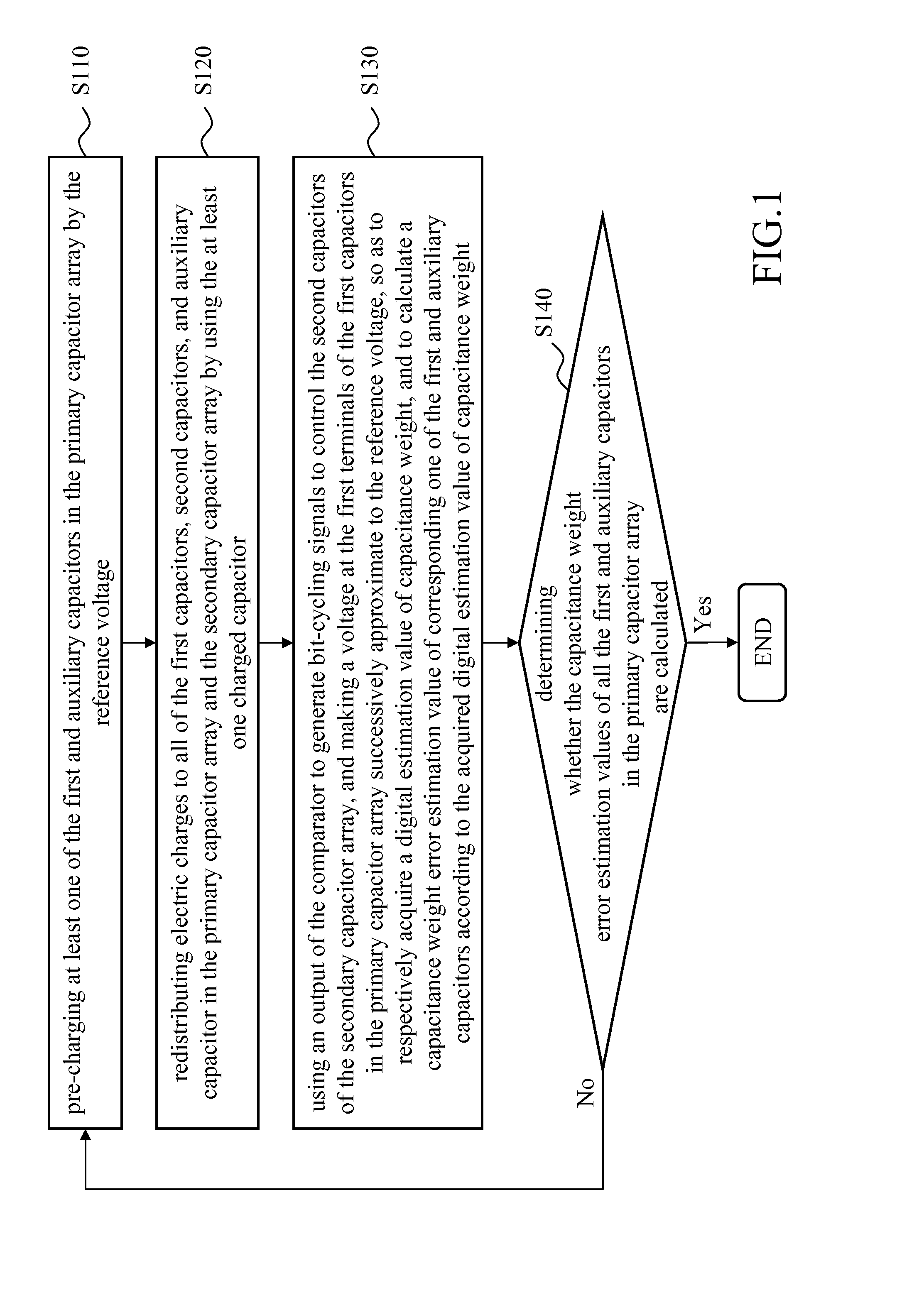
This non-provisional application claims priority under 35 U.S.C. §119(a) on Patent Application No(s). 101136974 filed in Taiwan, R.O.C. on Oct. 5, 2012, the entire contents of which are hereby incorporated by reference. 1. Technical Field The disclosure relates to the estimation of capacitance weight errors, more particularly to a full-digital capacitance weight error estimation method for estimating capacitance weight errors of a digital to analog converter (DAC) in a successive approximation analog to digital converter (ADC), and the successive approximation ADC using the same. 2. Related Art The ADC is widely used in communication equipments, measurement instruments, and other various electrical devices. Generally, the ADCs may be sorted as flash ADCs, pipelined ADCs, and successive approximation ADCs, etc. Because the successive approximation ADC may have low power consumption, it is widely used in all kinds of applications. The accuracy of the switched-capacitor type successive approximation ADC is mainly influenced by the capacitance weight errors. The smaller the capacitance weight errors are, the higher the accuracy of the successive approximation ADC is. However, in the manufacturing processes of the integrated circuits, the capacitance weight errors are unavoidable because of manufacturing process offsets. Therefore, it is the key point for the integrated circuit design to calibrate the capacitance weight errors caused by the manufacturing process offsets, so as to increase the accuracy of the successive approximation ADC. A conventional technique to calibrate the capacitance weight error is using precision instruments for measuring the actual capacitance value, then using the focused ion beam (FIB) manner for connecting with capacitors in parallel to increase the capacitance value thereof, or using the laser trimming manner for eliminating parallel capacitors to reduce the capacitance value thereof, until the capacitance value thereof matches the expected value, which means the calibration of the capacitance value is done. For either the laser trimming manner or the FIB manner, it is necessary to use extra manpower and equipment resources for calibrating the chipped integrated circuits. This causes extra expenses and enormous time may be required, which increase the manufacturing costs. Another conventional technique uses a resistor type DAC for generating an analog calibration voltage. After the analog calibration voltage supplies to a terminal of the calibrated capacitor, by changing the digital input code of the DAC, the voltage outputted by another terminal of the calibrated capacitor may be similar to the output voltage of the ideal capacitor without the calibration voltage. Afterward, the digital input code corresponding to the calibration voltage is stored. When the calibrated capacitor needs to be used, the digital input code is converted into the corresponding analog calibration voltage, for compensating the capacitor. However, because the actual implemented circuits can only generate positive voltages, thus the above resistor type calibration manner is only suitable for the actual capacitance value smaller than the ideal capacitance value. That is, the above manner can only perform the one-sign calibration of the capacitance weight errors. In addition, the above manner needs an extra resistor type DAC. Thus, extra hardware is required, and the errors generated by the resistor type DAC may also influence the accuracy after the calibration. The disclosure relates to a method for estimating capacitance weight errors of the DAC in a successive approximation ADC including a comparator, a capacitor set and a switch set. The capacitor set includes a primary capacitor array and a secondary capacitor array. The primary capacitor array includes an auxiliary capacitor and a plurality of first capacitors. The secondary capacitor array includes a low-weighted capacitor array including a plurality of second capacitors which respectively have known capacitance weights. The method includes the following steps. (A) At least one capacitor in the primary capacitor array is pre-charged by a first reference voltage. (B) Electric charges are redistributed to all of the first capacitors and the auxiliary capacitor in the primary capacitor array and to the second capacitors in the secondary capacitor array. (C) The second capacitors in the secondary capacitor array are controlled according to bit-cycling signals generated by an output of the comparator, and a voltage at first terminals of the first capacitors in the primary capacitor array successively approximates to a first reference voltage, so as to respectively acquire a digital estimation value of the capacitance weight, and to calculate a capacitance weight error estimation value of corresponding one of the first capacitors and the auxiliary capacitor according to the acquired digital estimation value of capacitance weight and the known capacitance weights. (D) The capacitance weight error estimation values of all the first capacitors and the auxiliary capacitor in the primary capacitor array are determined whether to be calculated or not, and if the capacitance weight error estimation values of all the first capacitors and the auxiliary capacitor in the primary capacitor array are not calculated, the steps (A), (B) and (C) are repeated until the capacitance weight error estimation values of all the first capacitors and auxiliary capacitor in the primary capacitor array are calculated. The disclosure also relates to a successive approximation ADC including a comparator, a capacitor set, a switch set and a controller. The comparator has a first input terminal, a second input terminal and an output terminal. The first input terminal of the comparator is for being supplied with the first reference voltage. The capacitor set includes a primary capacitor array and a secondary capacitor array. The primary array includes a plurality of first capacitors and an auxiliary capacitor. The capacitance weight of the smallest capacitor of the first capacitors is 1, and the capacitance weight of the auxiliary capacitor is smaller than 1. Each of the first capacitors and the auxiliary capacitor has a first terminal and a second terminal. The secondary capacitor array includes a plurality of second capacitors, and the capacitance weights of the second capacitors are binary-weighted. Each second capacitor has a first terminal and a second terminal. The first terminal of each first capacitor in the primary capacitor array is electrically connected to the second input terminal of the comparator. The first terminal of the auxiliary capacitor is electrically connected to the second input terminal of the comparator. The first terminal of each second capacitor in the secondary capacitor array is electrically connected to the second input terminal of the comparator. The second terminals of the first capacitors, the auxiliary capacitor and the second capacitors are electrically connected to the switch set. The secondary capacitor array further includes an attenuation capacitor. The second capacitors are connected to the second input terminal of the comparator through the attenuation capacitor. The capacitance weight of the attenuation capacitor is 1. The attenuation capacitor has a first terminal and a second terminal. The first terminal of each second capacitor is connected to the second terminal of the attenuation capacitor, and the first terminal of the attenuation capacitor is connected to the second input terminal of the comparator. The switch set includes a plurality of switches which are connected with the second terminals of the first capacitors and the auxiliary capacitor in the primary capacitor array, and the second terminals of the second capacitors in the secondary capacitor array one to one. The switches respectively control the second terminals of the first capacitors, the auxiliary capacitor, and the second capacitors to be supplied with the first reference voltage or a second reference voltage. The controller is used for controlling the switch set to perform the following steps. (A) At least one capacitor in the primary capacitor array is pre-charged by the first reference voltage. (B) Electric charges are redistributed to all of the first capacitors and the auxiliary capacitor in the primary capacitor array and to the second capacitors in the secondary capacitor array, by using the charged capacitor. (C) The second capacitors in the secondary capacitor array are controlled according to bit-cycling signals generated by an output of the output terminal of the comparator, to make a voltage at first terminals of the first capacitors and the auxiliary capacitor in the primary capacitor array successively approximate to the first reference voltage, to respectively acquire a digital estimation value of the capacitance weight, and to calculate a capacitance weight error estimation value of corresponding one of the first capacitors and the auxiliary capacitor according to the acquired digital estimation value of the capacitance weight. (D) The steps (A), (B) and (C) are repeated until the capacitance weight error estimation values of all the first capacitors and the auxiliary capacitor in the primary capacitor array are calculated. The disclosure will become more fully understood from the detailed description given herein below for illustration only, and thus are not limitative of the disclosure, and wherein: The following embodiments explain the detail features, advantages, and objectives of the disclosure and the descriptions thereof are enough for one skilled in the art to understand and implement the technical contents of the disclosure. Moreover, the embodiments described below use the same symbol for representing the same or similar components. In step S130, an output of the comparator is used to generate bit-cycling signals for controlling the second capacitors in the secondary capacitor array, and the voltage at the first terminals of the first capacitors in the primary capacitor array is successively approximated to the reference voltage, so as to respectively acquire a digital estimation value of the capacitance weight, and to calculate a capacitance weight error estimation value of corresponding one of the first and auxiliary capacitors according to the acquired digital estimation value of the capacitance weight. In step S140, it checks whether the capacitance weight error estimation values of all the first capacitors and the auxiliary capacitor in the primary capacitor array are calculated or not. If the capacitance weight error estimation values of all the first and auxiliary capacitors in the primary capacitor array are not calculated, the steps S110, S120 and S130 are repeated until the capacitance weight error estimation values of all the first and auxiliary capacitors in the primary capacitor array are calculated. The above descriptions briefly explain how to estimate the capacitance weight error in the DAC of the successive approximation ADC. The following descriptions have further explanations along with the circuit structures of the successive approximation ADC. For making the embodiment clear, the following symbols are defined in advance, as shown in Nominally, the ratio of the capacitance weights of the capacitors C12to C7and the auxiliary capacitor CDis 25:24:23:22:21:1:<1. That is, the capacitance weights of the capacitors except the auxiliary capacitor are binary-weighted, and the capacitance weight of the capacitor C7is the smallest among these capacitors and is larger than the nominal capacitance weight of the auxiliary capacitor CD. However, because errors may be introduced to in the manufacturing process of capacitors, the actual capacitance weight ratios of the mentioned capacitors are not exactly scaled. Let the absolute capacitance values with errors of the capacitors C12to C7and the auxiliary capacitor CDbe represented as follows: The symbols The capacitor set includes the primary capacitor array 22 and the secondary capacitor array 24. The primary capacitor array 22 includes the capacitors C12to C7and an auxiliary capacitor CD. Each of the capacitors C12to C7and the auxiliary capacitor CDhas a first terminal and a second terminal. The secondary capacitor array 24 includes the attenuation capacitor Ccaland the capacitors C6to C0. Each of the capacitors C0to C6and the attenuation capacitor Ccalhas a first terminal and a second terminal. The first terminals (such as the terminal 22 The switch set 30 has a plurality of switches including the switches d12 to d0, dD, and dA. The switches d12 to d0 and dD are respectively connected to the capacitors C12to C0and the auxiliary capacitor CDone to one. That is, each switch only connects to one capacitor. Each switch has an input terminal, a first output terminal and a second output terminal. The input terminals of the switches d12 to d7 and dD are respectively connected to the second terminals (such as terminals 22 The first output terminals of the switches d12 to d0 and dD are supplied with the reference voltage VREF. The second output terminals of the switches d12 to d0 and dD are supplied with the reference voltage VSS(such as a ground voltage or a work voltage). The control signals outputted by the controller 50 control the above switches, so that the input terminals of the switches are selectively connected to the first output terminals or the second output terminals. For example, when the control signal is “0”, the input terminal of the switch is connected to the second output terminal thereof, which is supplied with the reference voltage VSS, and when the control signal is “1”, the input terminal of the switch is connected to the first output terminal which is supplied with the reference voltage VREF. However, the mentioned embodiments show only one kind of control manner, and the disclosure is not limited thereby. The switch dA also has an input terminal, a first output terminal and a second output terminal. The input terminal of the switch dA is connected to the first terminals (the terminals 22 The controller 50 is coupled to the output terminal of the comparator 40. The controller 50 sends control signals for controlling the operation of each switch in the switch set 30. The control steps executed by the controller 50 are described as follows. In The input terminal of the switch dD is connected to the first output terminal which is supplied with the reference voltage VREF, so that the two terminals of the auxiliary capacitor CDare supplied with the reference voltage VREF. The switches d12 to d0 respectively corresponding to the other capacitors C12to C0are supplied with the reference voltage VSS. In this embodiment, the auxiliary capacitor CDis the capacitor under test (CUT). That is, in this step, the reference voltage VREFcharges all of the capacitors including the capacitors C12to C0and the attenuation capacitor Ccal, except the auxiliary capacitor CD. Subsequently, in Next, in For example, the controller 50 may firstly transmit a signal set of {0000001} to the switches d0 to d6. If the reference voltage VREFis larger than the output voltage VDAC, the bit-cycling signal corresponding to switch d6 is set as “1”. If the reference voltage VREFis smaller than the output voltage VDAC, the bit-cycling signal corresponding to switch d6 is set as “0”. When the bit-cycling signal corresponding to switch d6 is set as “0”, the controller 50 transmits a signal set of {0000010} to the switches d0 to d6. Similarly, if the reference voltage VREFis larger than the output voltage VDAC, the bit-cycling signal corresponding to switch d5 is set as “1”. If the reference voltage VREFis smaller than the output voltage VDAC, the bit-cycling signal corresponding to switch d5 is set as “0”. Successively, each bit of the bit-cycling signals is set by a similar manner, and the digital estimation value of the capacitance weight of corresponding capacitor is acquired. The aforementioned operations are analyzed as follows. In the step of pre-charging as shown in where the VSis the voltage of the first terminals (the terminals 24 Take The second step of the digital estimation manner of the capacitance weight of the auxiliary capacitor CDis the redistribution of the electric charges as shown in where Vcalis the voltage of the first terminals (the terminals 24 The following steps conduct bit-cycling to successively approximate the voltage of the second input terminal of the comparator to that of the first input terminal of the comparator (22 where ccycis the sum of the capacitances of the capacitors of the secondary capacitor array 24 whose second terminals are supplied with the reference voltage VREF. According to the electric charge conservation principle, the following two functions are obtained: By rearranging the above two functions, the equation (3) is obtained as follows: Supposing VREF=Vdac, the equation (3) is simplified to be: On the other hand, the equation (1) is rewritten as: By (5) and (4), we have: where Wsubis defined as the capacitance weight of the secondary capacitor array, dcxis the corresponding digital estimation value of cxwhere cxis the capacitance weight of one of the first capacitors C12to C7and the auxiliary capacitor CD. In this embodiment, the digital estimation value dcxis in between 0 and 127. By substituting the conditions of the The symbol dcDis defined as the digital estimation value of the capacitance weight of the auxiliary capacitor CD. The dcDis the target digital code acquired in the bit-cycling processes. Accordingly, the digital estimation value of the capacitance weight of the auxiliary capacitor CDis estimated through the function (7). To calculate the capacitance weight error ΔcDbetween the actual capacitance cDand the nominal capacitance As set forth above, the foregoing descriptions are only exemplary embodiments, so that the bit-cycling signals used in the binary searching, and the number of capacitors does not limit the disclosure. After acquiring the digital estimation value of the capacitance weight of the auxiliary capacitor CD, the digital estimation processes of the capacitance weight of the capacitor C7may successively be executed. In The input terminal of the switch d7 connects with the first output terminal which is supplied with the reference voltage VREF, so that the two terminals of the capacitor C7are both supplied with the reference voltage VREF. The other capacitors, namely the capacitors C12to C0and the auxiliary capacitor CDare supplied with the reference voltage VSS. That is, cMprc=c7. In this embodiment, the capacitor C7is a CUT. That is, in this step, the reference voltage VREFis only used for charging the capacitor C7. Thus, cMprc=c7. Subsequently, in Because the input terminal of the switch dA is connected to the second output terminal (floating), the first terminals (the terminals 22 Next, in Let the final acquired bit-cycling code after bit-cycling be dc7. By (6) with the new definitions of cMprc=c7and cMset=cD, we have: By the above steps, the digital estimation value of the capacitance weight of the capacitor C7is expressed as: The capacitance weight error Δc7between the actual capacitance c7and the theoretical capacitance After acquiring the digital estimation of the capacitance weight of the capacitor C7, the digital estimations of the capacitance weights of the capacitors C8, C9, C10, C11, and C12are also acquired by using the similar manner. Specifically, when acquiring the digital estimation of the capacitance weight of the capacitor C8in the pre-charging step, the controller 50 transmits a signal set of {0010000} to the switches dD and d7 to d12, transmits a signal set of {0000000} to the switches d0 to d6, and transmits a signal of {1} to the switch dA. Herein, cMprc=c8. In the step of redistributing electric charges, the controller 50 transmits a signal set of {1100000} to the switches dD and d7 to d12, transmits a signal set of {0000000} to the switches d0 to d6, and transmits a signal of {0} to the switch dA. Herein, cMset=c7+cD. In the step of approximating successively, the controller 50 transmits a signal set of {1100000} to the switches dD and d7 to d12, successively transmits a plurality of signal sets of bit-cycling codes to the switches d0 to d6, and transmits a signal of {0} to the switch dA. By the aforementioned steps, we have: where dc8is the final bit-cycling code in this step. Then, the function (12) is substituted into the capacitance weight error representation function, and the actual capacitance value c8is expressed as: When acquiring the digital estimation of the capacitance weight of the capacitor C9, the controller 50 in the pre-charging step transmits a signal set of {0001000} to the switches dD and d7 to d12, transmits a signal set of {0000000} to the switches d0 to d6, and transmits a signal of {1} to the switch dA. Herein, cMprc=c9. In the step of redistributing the electric charges, the controller 50 transmits a signal set of {1110000} to the switches dD and d7 to d12, transmits a signal set of {0000000} to the switches d0 to d6, and transmits a signal of {0} to the switch dA. Herein, cMset=c8+c7+cD. In the step of approximating successively, the controller 50 transmits a signal set of {1110000} to the switches dD and d7 to d12, successively transmits a plurality of signal sets of bit-cycling codes to the switches d0 to d6, and transmits a signal of {0} to the switch dA. By the above steps, the digital estimation value of the capacitance weight of the capacitor C9is acquired. Let dc9be the final bit-cycling code in this step, and we have: By using the similar manner, c10, c11and c12are respectively expressed as: After acquiring the digital estimations of the capacitance weights of all the first capacitors, their capacitance weight errors ΔcDand Δc7to Δc12are expressed as: In this way, the capacitance weight errors ΔcDand Δc7to Δc12can be obtained. These capacitance weight errors can be used for calibrating the successive approximation ADC. The successive approximation ADC is described as below. The controller 50 can generate control signals for controlling the switches connected to the capacitors C12to C7and the auxiliary capacitor CDin the primary capacitor array 22 according to the binary searching algorithm, and can successively generate the digital-to-analog voltages, for example, (1/2)VREF, d12(1/2)VREF+(1/22)VREF, d12(1/2)VREF+d11(1/22)VREF+(1/23)VREFd12(1/2)VREF+d11(1/22)VREF+d10(1/23)VREF+(1/24)VREFand so on, wherein d12to d7respectively represent the bits successively outputted by the comparator 40. These digital-to-analog voltages and the above analog signals are used for generating digital signals which are the results of the analog to digital conversion. Because the capacitance weight errors of the capacitors C7to C12in the primary capacitor array 22 cause the deviations of the digital-to-analog voltages required by the binary searching algorithm, the capacitance weight errors Δc12to Δc7can be used for controlling the switches in the secondary capacitor array 24 to compensate the deviations, thereby generating more precise analog voltages for increasing the accuracy of the analog to digital conversion. The disclosure also uses the acquired weight information to calibrate the digital output of the successive approximation ADC in a digital manner. The relation between the output and input of the successive approximation ADC is expresses as: where qeis the quantified error caused in the analog to digital conversion, and CTis the equivalent total capacitance value at the second input terminal of the comparator. By the equation (16), the digital representation codes of the capacitance weight errors of all the first capacitors can be acquired. From the equation (17), the disclosure can obtain the accurate digital output result issued by digitally eliminating the quantified errors of the capacitance weight errors. In this embodiment, the capacitance weights of the capacitance values of the capacitors C12to C7and the auxiliary capacitor CDare nominally 25, 24, 23, 22, 21, 1 and <1 respectively, and the capacitance weights of the capacitance values of the capacitors C6to C0and Ccalare 26, 25, 24, 23, 22, 21, 1 and 1 respectively. The successive approximation ADC is not limited by the above embodiments. In In this embodiment, the weights of the capacitors C6to C0follows the smallest one of the capacitors C12to C7. For example, the capacitance weights of the capacitors C6to C0follow the weight of the capacitor C7. For instance, the capacitance weights of the capacitance values of the capacitors C12to C7and the auxiliary capacitor CDare 25, 24, 23, 22, 21, 1 and <1 respectively, the capacitance weights of the capacitance values of the capacitors C6to C0are 2−1, 2−2, 2−3, 2−4, 2−5, 2−6and 2−7respectively. The first terminals of the capacitors C12to C7in the capacitor set 20 are connected to the second input terminal (the negative input terminal) of the comparator 40, and the first terminals of the capacitors C12to C7in the capacitor set 21 are connected to the first terminal (the positive terminal) of the comparator 40. Thus, the successive approximation ADC 200 is a fully-differential design, and the output of the comparator 40 is a fully-differential bit-cycling signal. Furthermore, the capacitors C12to C7and the auxiliary capacitor CDin the capacitor set 20 respectively cooperate with the corresponding capacitors12to C7and the auxiliary capacitor CDin the capacitor set 21 to form differential capacitor pairs. For example, the capacitor C12in the capacitor set 20 is connected to the capacitor C12in the capacitor set 21 to form a differential capacitor pair, the capacitor C11in the capacitor set 20 is connected to the capacitor C11in the capacitor set 21 to form another differential capacitor pair, and the rest may be deduced by analogy. The capacitors C6to C0in the capacitor set 20 respectively cooperate with the corresponding capacitors C6to C0in the capacitor set 21 to form differential capacitor pairs. For example, the capacitor C6in the capacitor set 20 cooperates with the capacitor C6in the capacitor set 21 to form a differential capacitor pair, the capacitor C5in the capacitor set 20 cooperates with the capacitor C5in the capacitor set 21 to form another differential capacitor pair, and the rest may be deduced by analogy. Moreover, the step of pre-charging in this embodiment causes that the voltage between the two input terminals of the comparator converges to VREF/2 after the bit-cycling operation. In this way, when the successive approximation ADC 200 in this embodiment acquires the digital estimation values of the capacitance weights of capacitors, the fully-differential manner is used for estimating the weight of each differential capacitor pair in the capacitor sets 20 and 21. In addition, the successive approximation ADC 200 can further include the attenuation capacitor Ccalshown in As set forth above, this disclosure can estimate the capacitance weights and capacitance weight errors of the capacitors, and calibrate the successive approximation ADC and perform the analog to digital conversion by using the same circuit structure. In addition, the capacitance weight errors of the capacitors can directly be stored in digital form and then be used for calibrating the result of the analog to digital conversion. It is not necessary for the disclosure to using extra DACs, thereby reducing the capacitance weight errors caused in the digital to analog conversion. Therefore, the successive approximation ADC in the disclosure may have a higher accurate result of the analog to digital conversion than the conventional hardware structure. A method for estimating capacitance weight errors of a digital-to-analog converter and a successive approximation (SA) analog-to-digital converter (ADC) using the same are disclosed, and the SA ADC includes a comparator, a capacitor set, a switch set and a controller. The capacitor set includes a primary capacitor array including a plurality of binary-weighted capacitors, and a secondary capacitor array including a plurality of binary-weighted capacitors with known capacitance weights. The controller controls the switch set and repeats the steps of pre-charging the primary capacitor array, redistributing electric charges to the primary capacitor array and the secondary capacitor array, and performing a successive approximation binary searching on the primary capacitor array and the secondary capacitor array to calculate the capacitance weight error of each capacitor in the primary capacitor array. The calculated capacitance weight errors are used for calibrating the output of the successive approximation ADC. 1. A method for estimating capacitance weight errors of a digital to analog converter (DAC) in a successive approximation analog to digital converter (ADC) including a comparator, a capacitor set and a switch set, the capacitor set including a primary capacitor array and a secondary capacitor array, the primary capacitor array including a plurality of first capacitors and an auxiliary capacitor, and the secondary capacitor array including a low-weighted capacitor array having a plurality of known second capacitors, the method comprising:
(A) pre-charging at least one of the first and auxiliary capacitors in the primary capacitor array by a first reference voltage; (B) redistributing electric charges to the first and auxiliary capacitors in the primary capacitor array and to the second capacitors in the secondary capacitor array, by using the at least charged one of the first and auxiliary capacitors; and (C) using an output of an output terminal of the comparator to generate bit-cycling signals for controlling the second capacitors in the secondary capacitor array and making voltages of the first and auxiliary capacitors in the primary capacitor array successively approximate to the first reference voltage, so as to respectively acquire a digital estimation value of capacitance weight, and to calculate a capacitance weight error estimation value of corresponding one of the first and auxiliary capacitors according to the acquired digital estimation value of the capacitance weight. 2. The method for estimating capacitance weight errors of the DAC in the successive approximation ADC according to (D) determining whether the capacitance weight error estimation values of the first and auxiliary capacitors in the primary capacitor array are calculated or not and if the capacitance weight error estimation values of the first and auxiliary capacitors in the primary capacitor array are not calculated, returning to the step (A) and repeating the steps (A), (B) and (C) until the capacitance weight error estimation values of the first and auxiliary capacitors in the primary capacitor array are calculated. 3. The method for estimating capacitance weight errors of the DAC in the successive approximation ADC according to 4. The method for estimating capacitance weight errors of the DAC in the successive approximation ADC according to 5. The method for estimating capacitance weight errors of the DAC in the successive approximation ADC according to controlling the first terminals of the first and auxiliary capacitors in the primary capacitor array to be supplied with the first reference voltage; transmitting a control signal to the switch set for setting one of the first and auxiliary capacitors to be a capacitor under test (CUT) which is supplied with the first reference voltage through the switch set; and controlling a part of the first and auxiliary capacitors except the CUT in the primary capacitor array to be supplied with the second reference voltage. 6. The method for estimating capacitance weight errors of the DAC in the successive approximation ADC according to controlling the first terminals of the first capacitors and the auxiliary capacitor in the primary capacitor array to be floating; controlling the CUT to be supplied with the second reference voltage through the switch set; and controlling the part of the first and auxiliary capacitors except the CUT in the primary capacitor array to be supplied with the first reference voltage through the switch set. 7. The method for estimating capacitance weight errors of the DAC in the successive approximation ADC according to wherein dcxrepresents the digital estimation value, cMprcrepresents a sum of the capacitance values of the primary capacitor array supplied with the first reference voltage in step (A), cMsetrepresents a sum of the capacitance values of the primary capacitor array supplied with the first reference voltage in step (B), ccalrepresents the capacitance value of the attenuation capacitor, cStotalrepresents a sum of the capacitance values of the second capacitors in the secondary capacitor array, ccycrepresents a sum of the capacitance values of the second capacitors supplied with the first reference voltage through the switch set, c0represents a minimum capacitance value in the secondary capacitor array, and Wsubrepresents the capacitance weight of the secondary capacitor array. 8. The method for estimating capacitance weight errors of the DAC in the successive approximation ADC according to 9. The method for estimating capacitance weight errors of the DAC in the successive approximation ADC according to 10. A successive approximation ADC, comprising:
a comparator having a first input terminal, a second input terminal and an output terminal, wherein the first input terminal is supplied with a first reference voltage; a capacitor set comprising a primary capacitor array and a secondary capacitor array, the primary capacitor array comprising a plurality of first capacitors and an auxiliary capacitor, each of the first and auxiliary capacitors having a first terminal and a second terminal, the secondary capacitor array comprising a plurality of second capacitors, each of the second capacitors having a first terminal and a second terminal, the first terminals of the first capacitors being electrically connected to the second input terminal of the comparator, the first terminal of the auxiliary capacitor being electrically connected to the second input terminal of the comparator, and the first terminals of the second capacitors being electrically connected to the second input terminal of the comparator, wherein a capacitance weight of one first capacitor with a minimum capacitance value in the first capacitors is 1, a capacitance weight of the auxiliary capacitor is smaller than 1, and capacitance weights of the second capacitors are binary-weighted; a switch set comprising a plurality of switches which are respectively connected with the second terminals of the first and auxiliary capacitors in the primary capacitor array and the second terminals of the second capacitors, each of the switches respectively controlling the second terminals of the first, second and auxiliary capacitors to be supplied with the first reference voltage or a second reference voltage; and a controller, for controlling the switch set, and performing the following steps:
(A) pre-charging at least one of the first capacitors in the primary capacitor array by the first reference voltage; (B) by using at least one charged capacitor, redistributing electric charges to the first and auxiliary capacitors in the primary capacitor array and to the second capacitors in the secondary capacitor array; and (C) controlling the second capacitors in the secondary capacitor array according to bit-cycling signals outputted by an output of the output terminal of the comparator, and making a voltage at the first terminals of the first capacitors in the primary capacitor array successively approximate to the first reference voltage, so as to acquire a digital estimation value of the capacitance weight, and to calculate a capacitance weight error estimation value of corresponding one of the first and auxiliary capacitors according to the acquired digital estimation value of the capacitance weight. 11. The successive approximation ADC according to (D) repeating the steps (A), (B) and (C) until the controller obtains the capacitance weight estimation values of the first and auxiliary capacitors in the primary capacitor array. 12. The successive approximation ADC according to 13. The successive approximation ADC according to 14. The successive approximation ADC according to 15. The successive approximation ADC according to controlling the first terminals of the first capacitors and the first terminal of the auxiliary capacitor to be supplied with the first reference voltage; transmitting a control signal to the switch set for making either one first capacitor or the auxiliary capacitor to be a CUT and be supplied with the first reference voltage through the switch set; and controlling the first capacitors and the auxiliary capacitor except the CUT in the primary capacitor array to be supplied with the second reference voltage through the switch set. 16. The successive approximation ADC according to controlling the first terminals of the first and auxiliary capacitors in the primary capacitor array to be floating; controlling the CUT to be supplied with the second reference voltage through the switch set; and controlling the first and auxiliary capacitors except the CUT in the primary capacitor array to be supplied with the first reference voltage through the switch set. 17. The successive approximation ADC according to wherein dcxrepresents the digital estimation value, cMprcrepresents a sum of the capacitance values in the primary capacitor array supplied with the first reference voltage in step (A), cMsetrepresents a sum of capacitance values of the first capacitors and the auxiliary capacitor in the primary capacitor array supplied with the first reference voltage in step (B), ccalrepresents a capacitance value of the attenuation capacitor, cStotalrepresents a sum of capacitance values of the second capacitors in the secondary capacitor array, ccycrepresents a sum of the capacitance values of the second capacitors which are supplied with the first reference voltage through the switch set, c0represents the minimum one of the capacitance values of the second capacitors in the secondary capacitor array, and Wsubrepresents the capacitance weight of the secondary capacitor array.CROSS-REFERENCE TO RELATED APPLICATIONS
BACKGROUND
SUMMARY
BRIEF DESCRIPTION OF THE DRAWINGS
DETAILED DESCRIPTION
(
Δ
Δ
Δ
Δ
Δ
Δ
Δ
Δ