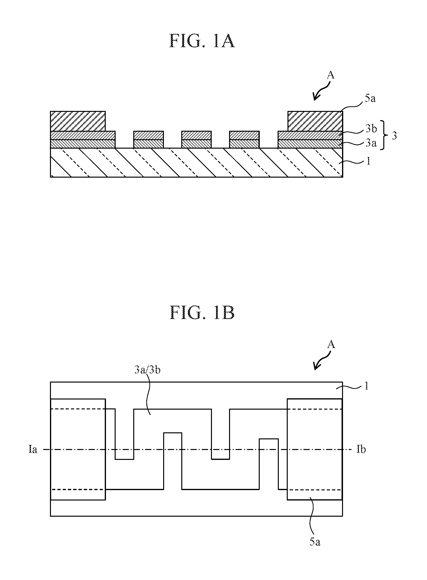
THIN-FILM RESISTOR AND METHOD FOR PRODUCING THE SAME
The present application claims priority from Japanese patent application JP 2015-136373 filed on Jul. 7, 2015, the content of which is hereby incorporated by reference into this application. 1. Field of the Invention The present invention relates to a thin-film resistor and a method for producing the same. 2. Description of the Related Art Resistors are used for many electronic devices such as personal computers and portable terminals. In particular, thin-film resistors with high reliability are required for automobiles, medical devices, and industrial machines such as robots. Such resistors have been required to have reduced chip sizes with a reduction in the size of electronic devices in recent years, and even resistors with reduced chip sizes are required to have equal resistance values to those of the conventional resistors. To that end, reducing the thickness of a film of a resistive material or reducing the size of a resistor pattern (i.e., reducing the thickness of a line pattern) is considered. However, reducing the thickness of a film or reducing the thickness of a line pattern too much can decrease the long-term reliability and deteriorate the characteristics of the thin-film resistor. Therefore, it is basically necessary to obtain a resistive material with higher specific resistance (i.e., resistivity). As a thin-film resistive material with high specific resistance, a material that contains chromium and silicon and also contains a valve metal or a transition metal added thereto is disclosed, for example (see Patent Document 1). Specifically, Patent Document 1 discloses a material that contains one or more of metals selected from Nb, Ta, Al, Cu, Mn, Zr, or Ni in addition to chromium and silicon. A target containing a thin-film resistive material is sputtered so that the material is deposited on the surface of a substrate as a resistive film. Sputtering is performed with a mixed gas of argon and nitrogen that are inert gases. Increasing the percentage of the nitrogen gas can form a resistive film with relatively high specific resistance. The resistive film deposited on the substrate is patterned into a shape that can obtain approximately a desired resistance value through photolithography or the like, and the resistive film is then subjected to heat treatment under an inert gas atmosphere such as nitrogen or argon. Adequately setting the conditions of the heat treatment can obtain a low (approximately zero) temperature coefficient of resistance (TCR). The thus produced resistive film exhibits a specific resistance of about several mΩ·cm, and has a resistance value of about several hundred kΩ·cm to 1 MΩ·cm as a thin-film resistor. Such a resistive film has a temperature coefficient of resistance TCR in the range of about ±25 ppm/° C., for example. 3. Related Art Documents Patent Document 1: JP 2002-141201 A As described above, there has been a demand for increasing resistivity. As a method for increasing the specific resistance of a resistive film, there is known a method of increasing the amount of a nitrogen gas used for sputtering and thus increasing the amount of silicon nitride with high specific resistance. However, a resistive film formed with such a method has a problem in that the characteristics of the negative TCR of the silicon nitride become dominant, and thus that if the specific resistance is attempted to be increased, it would be difficult to set the TCR to approximately zero. It is an object of the present invention to provide a thin-film resistor that has a higher resistance value than the conventional thin-film resistors while retaining excellent TCR characteristics. According to an aspect of the present invention, there is provided a thin-film resistor including a substrate, a pair of electrodes formed on the substrate, and a resistive film connected to the pair of electrodes. The resistive film includes a first resistive film and a second resistive film, the second resistive film having a different TCR from that of the first resistive film, and each of the first resistive film and the second resistive film contains Si, Cr, and N as the main components. One of the first resistive film or the second resistive film preferably has a positive TCR value, and the other preferably has a negative TCR value. The first resistive film and the second resistive film contain different percentages of silicon nitride across (on the two different sides of) xTCR (a threshold of silicon nitride, which may have some range) as a boundary, the xTCR being the percentage of silicon nitride at which a positive TCR changes to a negative TCR or a negative TCR changes to a positive TCR. Each of the first resistive film and the second resistive film contains silicon nitride, and the percentage of Si that forms silicon nitride in the first resistive film relative to the entire Si contained in the first resistive film is preferably less than or equal to 63%, and the percentage of Si that forms silicon nitride in the second resistive film relative to the entire Si contained in the second resistive film is preferably greater than or equal to 68%. In the first resistive film, chromium silicide crystallites are continuously formed and structured, and a network structure is thus formed with the crystallites joined together. Such a structure can realize a film with high conductivity and low sheet resistance. In the second resistive film, it is found that chromium silicide crystallites are individually dispersed to form a discontinuous structure. Such a structure can realize a film with low conductivity and high sheet resistance. The second resistive film may contain added thereto at least one metal element selected from Ti, Zr, or Al. The metal element added is preferably contained at a percentage of 1 to 4 atm % relative to the entire second resistive film. Such elements are elements that will easily form nitride. Such elements are added to adjust the characteristics of the resistive film. It is also possible to adjust the characteristics of the resistive film by adding as a main component an element that is unlikely to form nitride instead of Cr. For example, the present invention may be a thin-film resistor including a substrate, a pair of electrodes formed on the substrate, and a resistive film connected to the pair of electrodes. The resistive film may include a first resistive film and a second resistive film, the second resistive film having a different TCR from that of the first resistive film. The first resistive film may contain Si, Cr, and N as the main components, and the second resistive film may contain Si, N, and a metal element that is to form silicide but is unlikely to form nitride. The metal element is preferably at least one element selected from Mo, W, Fe, or Co. According to another aspect of the present invention, there is provided a method for producing a thin-film resistor including a substrate, a pair of electrodes formed on the substrate, and a resistive film connected to the pair of electrodes, the method including forming a first resistive film containing Si, Cr, and N as the main components, and forming a second resistive film containing Si, Cr, and N as the main components in a stacked manner on the first resistive film. The first resistive film and the second resistive film are formed by sputtering in an atmosphere containing nitrogen, and the mixture ratio of the nitrogen is increased in forming one of the first resistive film or the second resistive film. The present invention also provides a method for producing a thin-film resistor including a substrate, a pair of electrodes formed on the substrate, and a resistive film connected to the pair of electrodes, the method including forming a first resistive film containing Si, Cr, and N as the main components; and forming a second resistive film containing Si, Cr, and N as the main components in a stacked manner on the first resistive film. The first resistive film and the second resistive film are formed by sputtering in a gas containing nitrogen, and one of the first resistive film or the second resistive film is formed using a target containing at least one added metal element selected from Ti, Zr, or Al. According to the present invention, a thin-film resistor can be provided that has a higher resistance value than the conventional thin-film resistors while retaining excellent TCR characteristics. In this specification, the phrase “containing Si (silicon), Cr (chromium), and N (nitrogen) as the main components” means that only Si, Cr, N are the elements that are intentionally contained as the components and the other components are so-called dopant components or unintended impurities that are contained at about 5 atm %, for example. In addition, although “sheet resistance” and “specific resistance (resistivity)” differ in practice, they have the same meaning as long as the film thickness is constant. Thus, such terms may be used interchangeably in this specification. Hereinafter, a resistor and a method for producing the resistor in accordance with an embodiment of the present invention will be described in detail with reference to the drawings. The first resistive film 3 Hereinafter, a method for producing the resistor illustrated in As illustrated in The first resistive film 3 It should be noted that reducing the thickness of the resistive film more can also increase the sheet resistance of the resistive film and thus can increase the resistance value of the resulting resistor. However, as the surface of the substrate 1 has relatively large irregularities and a resistive film that is formed too thin on such surface is likely to be influenced by the variation in the thickness, the resistive film should have a certain thickness in order to produce a resistor stably. Next, the second resistive film 3 The second resistive film 3 Next, the resistive film with the stacked first resistive film 3 Next, the substrate 1 with the resistive film pattern formed thereon is subjected to heat treatment under an inert gas atmosphere such as nitrogen or argon. The detailed conditions of the heat treatment step and the like will be described later. The first resistive film 3 The suitable percentage of silicon that forms nitride in the first resistive film 3 As described above, the second resistive film 3 Next, a base electrode is formed ( The substrate 1, which has the pattern of the resistive thin film 3 formed thereon, is coated with photoresist, which is then patterned. After that, the patterned surface of the resistive thin film is sputter-etched by about several nm using argon ions or the like. This step is performed to remove a natural oxide film formed on the surface of the resistive thin film in the heat treatment step and the like and thus obtain an excellent electrical conduction between the resistive thin film 3 and the base electrode 5 After that, the photoresist is peeled away using an organic solvent such as a release agent so that copper films are formed as the base electrode 5 Next, a silicon oxide film 11 is formed as a protective film using a plasma CVD apparatus, for example, ( It is also possible to deposit a silicon nitride protective film using a plasma CVD apparatus before forming the silicon oxide film 11 as a protective film. Alternatively, it is also possible to deposit a silicon nitride protective film (not shown) using a plasma CVD apparatus after forming the protective film. In the step of forming a silicon nitride protective film, SiH4, NH3, or N2gas is used as a source gas. The thickness of the silicon nitride protective film may be about 50 to 100 nm. As the silicon nitride protective film has lower moisture permeability than the silicon oxide film, it is possible to suppress intrusion of moisture even under a high-temperature, high-humidity environment. After that, the protective film 11 (i.e., the silicon oxide film or a stacked film of the silicon oxide film and the silicon nitride film) is patterned using a photolithography technique so as to form an opening above at least the base electrode 5 Next, a primary breaking process is performed to split the substrate 1 into strip-like chip groups. Then, an end-surface base electrode 21 is formed on an exposed end surface of the substrate ( In order to form a resistive film, a sputtering technique is used, for example. When sputtering is performed using a target, a mixed gas that contains appropriate amounts of an inert gas and nitrogen is preferably used to obtain a film with high specific resistance. Herein, a mixed gas of argon and nitrogen is used, and the mixture ratio (i.e., flow rate) of nitrogen in the gas may be set in the range of about 10 to 30%, for example. Accordingly, a film that contains an appropriate amount of silicon contained in the target, which has been nitrided, is deposited on the substrate, and a resistive film is thus obtained. The suitable percentage of nitrogen contained in the first resistive film is about 20 to 26 atm %, and about 50 to 63% of silicon contained in the resistive film is preferably nitrided. It should be noted that as the first resistive film and the second resistive film may be arranged in any order in the vertical direction, the mixture ratio of nitrogen may be adjusted such that the mixture ratio of nitrogen in the first resistive film 3 At the percentage of the metal element and the percentage of the nitrogen gas used for sputtering, the second resistive film 3 Hereinafter, the heat treatment step described briefly above will be described in detail. The substrate 1 that has the resistive film pattern 3 (3 The inventor has found through a research that such a structure is greatly related to the electrical characteristics (specific resistance or TCR) of the resistive films 3 The resistive films 3 However, when heat treatment is performed at a temperature of greater than or equal to 500° C., chromium aggregates within the resistive films 3 Herein, chromium silicide has positive TCR characteristics, while silicon nitride that is a matrix has negative TCR characteristics. If the heat treatment temperature is relatively low, chromium silicide crystallites are not formed sufficiently. Thus, the TCR characteristics of the entire resistive films remain negative. If the heat treatment temperature is increased, the formation of chromium silicide crystallites is promoted, and the TCR changes to a value of approximately zero or to a positive value. When the heat treatment temperature is further increased, the formation of chromium silicide crystallites is further promoted, so that phase separation between the chromium silicide crystallites and the silicon nitride matrix portion is promoted. Electric charge preferentially moves through the chromium silicide crystallites with relatively low resistance. Thus, the characteristics of the chromium silicide dominate the TCR of the resistive films and thus change the TCR to a higher positive value. Concurrently, the portions of the chromium silicide crystallites aggregate and form a thin, long structure, which in turn increases the resistance of the films. The results of the detailed consideration will be described below. As is understood from By the way, in the conventional art where a resistive film has a single layer, heat treatment is performed to a target temperature at which the TCR characteristics become approximately zero. Thus, the obtained specific resistance has a relatively low value. In addition, as is understood from In this embodiment, heat treatment is performed at a temperature higher than that when a condition where the TCR characteristics become approximately zero is targeted as in conventional art. Accordingly, it is possible to form the first resistive film 3 As is understood from The percentage of nitrogen in the second resistive film 3 Consequently, electric charge flows not only through the chromium silicide crystallites but also through the silicon nitride portions (i.e., matrix region) between the crystallites. Thus, such electric charge is strongly influenced by the high specific resistance and the negative TCR characteristics of the region. In this embodiment, the first resistive film 3 The sheet resistance Rs1 of the resistive film 3, which is obtained by stacking the first resistive film 3 As shown in Formula (1), the sheet resistance Rs of the stacked resistive film 3 is lower than the sheet resistance Rs1 of the first resistive film 3 Thus, as long as appropriate Rs2 is obtained, it is possible to realize the sheet resistance Rs that is sufficiently higher than that of the conventional single-layer structure. When the proportion of Rs relative to Rs1 is generalized as n (0<n<1), it can be represented by Formula (2) below. Formula (2) can be deformed into Formula (3). From such formula, it is found that in order to set Rs to be greater than or equal to a half of Rs1 (n≧0.5), it is acceptable as long as Rs1≦Rs2 is satisfied. In such a case, the sheet resistance Rs becomes about five times that of the conventional resistive layer with a single-layer structure. In addition, in order to set Rs to be greater than or equal to 95% of Rs1 (n≧0.95), it is acceptable as long as the composition (i.e., nitrogen content) and the film thickness of the second resistive film 3 Next, the resistance/temperature characteristics TCR of the stacked resistive film 3 will be described. It is assumed that the sheet resistance of the first resistive film 3 The sheet resistance Rs at the temperature T of the stacked resistive film 3, which is obtained by stacking the first resistive film 3 From the above, the variation amount Rs(T+ΔT)−Rs(T) of the combined resistance when the temperature is changed from T to T+ΔT is obtained as follows. By assigning this combined resistance Rs to the equation of TCR, the following equations are obtained. Thus, the TCR of the stacked resistive film 3 is represented by Formula (5) below. Here, the following relationship is used (i=1, 2) From Formula (5), it is found that in order to set the TCR of the resistive film 3 to approximately zero, it is acceptable as long as the number in brackets of the numerator of Formula (5) is set zero. Herein, when the temperature coefficient of resistance TCR2 of the second resistive film 3 For example, when n=0.95, the allowable margin of variation in TCR2 can be increased than when n=0.5. Thus, the production of the second resistive film 3 From the results of the consideration above, in order to obtain desired sheet resistance Rs, appropriate Rs1 and n are determined in accordance with Formula (2). The value of n at this time is desirably as large as possible within the range of 0.5≦n<1. From the thus determined n and TCR1 that is obtained when the first resistive film 3 Alternatively, it is also possible to determine the heat treatment conditions in accordance with Formula (6), taking into consideration TCR1 and TCR2 that change in accordance with the heat treatment conditions, within the range that 0.5≦n<1 is satisfied or preferably such that n becomes as large as possible. In accordance with the thus obtained n, the specific resistance and the film thickness of the first resistive film 3 Such heat treatment conditions are, for example, greater than or equal to 500° C. or desirably greater than or equal to 750° C. The upper limit is estimated to be 1000° C. If heat treatment is performed in a region of up to a temperature region where the TCR does not fluctuate any further in the production stage, it is possible to suppress the fluctuations in the TCR thereafter and thus obtain a resistive film with stable TCR as a whole. When the first resistive film 3 Hereinafter, the compositions and the like of the first resistive film 3 The first resistive film 3 The suitable percentage of silicon that forms nitride in the first resistive film 3 The reason for setting the percentage of silicon in each resistive film in the aforementioned range is as follows. When silicon nitride in the first resistive film 3 Meanwhile, when silicon nitride in the second resistive film 3 The value in the range of 63 to 68% that is between the percentage of silicon that forms nitride in the first resistive film 3 As illustrated in If the nitrogen content in the first resistive film 3 The first resistive film 3 As described above, the first resistive film 3 As the second resistive film 3 It is found that as the second resistive film 3 With respect to the first resistive film 3 Moreover, it was discovered that among such resistive films each containing chromium, silicon, and nitrogen as the main components, such a difference in the direction in which the TCR changes is generated abruptly when the percentage of silicon nitride is between 63 to 68% (see In this specification, the percentage of silicon nitride at which the direction in which the TCR changes is reversed in such a newly discovered phenomenon is referred to as xTCR (a threshold of the percentage of silicon nitride related to the TCR). Such xTCR is an important parameter that influences the sheet resistance-TCR characteristics of the two-layer resistive film in this embodiment. With respect to such a phenomenon, the inventor has estimated the following mechanism so far. In a resistive film that contains chromium, silicon, and nitrogen as the main components, the formation of chromium silicide crystallites in the resistive film is promoted with an increase in the heat treatment temperature. Chromium silicide has a positive TCR, and electric charge preferentially flows through such crystallites. Thus, the first resistive film 3 However, if the nitrogen content in the resistive film is increased and the percentage of silicon nitride (matrix) is thus increased, a structure in which crystallites are individually dispersed is formed, in which case electric charge flows through the crystallites as well as the silicon nitride regions between the crystallites. As the silicon nitride regions have high resistance and a negative TCR, the characteristics of the resistive film change to negative. Furthermore, as a change in the structure of the resistive film that depends on the silicon nitride content occurs uniformly across the entire film, the TCR will abruptly change even when there is a slight change in the nitrogen content (i.e., silicon nitride content) around xTCR. As described above, the first and second resistive films with different TCRs are stacked. When a stacked resistive film of the first and second resistive films, which each contain Si, Cr, and N as the main components and contain different percentages of N, is used, it is possible to realize a resistive film that has a higher resistance value than the conventional resistive films and has a TCR of around zero. It is also possible to reduce the size of the resulting thin-film resistor. It should be noted that the phrase “has a higher resistance value than the conventional resistive films” means that it is possible to realize a high resistance value three times or more that of a resistor with a (single-layer) resistive film that contains chromium, silicon, and nitrogen as the main components. Next, a second embodiment of the present invention will be described. The first resistive film 3 When one of the aforementioned metal elements that will form nitride is added to a resistive film that contains chromium, silicon, and nitrogen, the specific resistance and the TCR characteristics of the resistive film will change. For example, there is seen a tendency that when Nb, Ta, or the like is added, the specific resistance of the resistive film will decrease and the TCR will change in the negative direction. Meanwhile, it was observed that in a resistive film that contains Ti, Zr, Al, or the like added thereto, the specific resistance changes only a little or does not change almost at all, and the TCR changes in the negative direction. It is considered that such a difference in the change in the characteristics of the resistive films that depend on the added elements is related to how easily nitride of the added element can be formed. Ti, Zr, and Al are elements that can easily form nitride in comparison with Nb and Ta. As an example, It is found that a resistive film with Ti added thereto has negative TCR characteristics. It is also found that such characteristics change in accordance with the amount of Ti added. The percentage of a nitrogen gas contained in the sputtering gas (Ar+N2gas) used for forming the first resistive film 3 When such a method is used, the first resistive film 3 When such a metal element is added, the specific resistance (i.e., sheet resistance) will also change. The amount of the metal element added that does not cause a significant reduction in the specific resistance due to the addition is desirably in the range of about 1 to 4 atm %. As long as the added amount is within such a range, it is possible to adjust the specific resistance and the TCR characteristics of the second resistive film 3 When the amount of Ti added is greater than or equal to 4 atm %, the sheet resistance Rs2 will decrease, while when the amount of Ti added is less than or equal to 1 atm %, the TCR2 will have a positive value. Thus, the amount of Ti added to the second resistive film 3 As described above, according to this embodiment, it is possible to easily set the TCR value to approximately zero while suppressing the fluctuations in the sheet resistance only by adding one of the aforementioned metal elements, which will form nitride, in an appropriate quantity, to a resistive film that contains chromium, silicon, and nitrogen. It should be noted that as described above, the percentage of a nitrogen gas contained in the sputtering gas used for forming the first resistive film 3 Next, a third embodiment of the present invention will be described. The first resistive film in this embodiment is characterized by containing chromium, silicon, and nitrogen, and the second resistive film is characterized by containing silicon, nitride, and a metal element that will form silicide but is unlikely to form nitride. As a metal element that will form silicide but is unlikely to form nitride, Mo, W, Fe, and Co can be used. When a second resistive film containing such a metal element is formed and is subjected to heat treatment, silicide of the metal element is formed in the resistive film. The inventor studied and found that the specific resistance (i.e., sheet resistance) and the TCR characteristics of the second resistive film will change in accordance with the type and the amount of a metal element used. In order to realize a resistive film with about the same specific resistance as that when chromium is used as in the first and second embodiments, the percentage of a metal element that will form silicide but is unlikely to form nitride is desirably between about 15 and 22 atm %. In this embodiment, an element that is unlikely to form nitride and will easily form silicide, like chromium, is used as a substitute element for chromium for the second resistive film 3 Further, the percentage of a nitrogen gas contained in the sputtering gas used for forming the first resistive film and that for forming the second resistive film are preferably the same. Accordingly, advantages that are similar to those described in the second embodiment are provided. The percentage of a metal element that will form silicide but is unlikely to form nitride as well as the percentage of a nitrogen gas used for sputtering is preferably set at a level that allows the second resistive film to have a negative TCR value and have about the same specific resistance as that of the first resistive film. When an appropriate element is selected within the range of the percentage, a second resistive film with desired characteristics can be formed. Using an oxygen gas instead of a nitrogen gas also has a possibility that similar advantageous effects may be obtained. In the aforementioned embodiments, configurations and the like that are illustrated in the attached drawings are not limited thereto, and can be changed as appropriate within the range that the advantageous effects of the present invention can be exerted. Besides, such configurations and the like can be changed as appropriate within the scope of the object of the present invention. Although a two-layer stacked structure has been exemplarily described above as the structure of the resistive film, the stacked structure may have three or more layers. Although examples of the application of the present invention to a chip resistor formed of a resistive film have been described above, the present invention can also be applied to a variety of components, such as an integrated circuit that uses a resistor. Each constituent element of the present invention can be selected or not selected as appropriate, and an invention that has the selected elements is also encompassed by the present invention. The present invention is applicable to a resistor. Provided is a thin-film resistor that has a higher resistance value than the conventional thin-film resistors while retaining excellent TCR characteristics. The thin-film resistor includes a substrate, a pair of electrodes formed on the substrate, and a resistive film connected to the pair of electrodes. The resistive film includes a first resistive film and a second resistive film, the second resistive film having a different TCR from that of the first resistive film, and each of the first resistive film and the second resistive film contains Si, Cr, and N as the main components. 1. A thin-film resistor comprising a substrate, a pair of electrodes formed on the substrate, and a resistive film connected to the pair of electrodes, wherein
the resistive film includes a first resistive film and a second resistive film, the second resistive film having a different TCR from that of the first resistive film, and each of the first resistive film and the second resistive film contains Si, Cr, and N as main components. 2. The thin-film resistor according to 3. The thin-film resistor according to 4. The thin-film resistor according to each of the first resistive film and the second resistive film contains silicon nitride, and a percentage of Si that forms silicon nitride in the first resistive film relative to the entire Si contained in the first resistive film is less than or equal to 63%, and a percentage of Si that forms silicon nitride in the second resistive film relative to the entire Si contained in the second resistive film is greater than or equal to 68%. 5. The thin-film resistor according to 6. The thin-film resistor according to 7. A thin-film resistor comprising a substrate, a pair of electrodes formed on the substrate, and a resistive film connected to the pair of electrodes, wherein
the resistive film includes a first resistive film and a second resistive film, the second resistive film having a different TCR from that of the first resistive film, and the first resistive film contains Si, Cr, and N as main components, and the second resistive film contains Si, N, and a metal element that is to form silicide but is unlikely to form nitride. 8. The thin-film resistor according to 9. A method for producing a thin-film resistor including a substrate, a pair of electrodes formed on the substrate, and a resistive film connected to the pair of electrodes, the method comprising:
forming a first resistive film containing Si, Cr, and N as main components; and forming a second resistive film containing Si, Cr, and N as main components in a stacked manner on the first resistive film, wherein the first resistive film and the second resistive film are formed by sputtering in an atmosphere containing nitrogen, and a mixture ratio of the nitrogen is increased in forming one of the first resistive film or the second resistive film. 10. A method for producing a thin-film resistor including a substrate, a pair of electrodes formed on the substrate, and a resistive film connected to the pair of electrodes, the method comprising:
forming a first resistive film containing Si, Cr, and N as main components; and forming a second resistive film containing Si, Cr, and N as main components in a stacked manner on the first resistive film, wherein the first resistive film and the second resistive film are formed by sputtering in an atmosphere containing nitrogen, and one of the first resistive film or the second resistive film is formed using a target containing at least one added metal element selected from Ti, Zr, or Al.RELATED APPLICATIONS
BACKGROUND OF THE INVENTION
Patent Documents
SUMMARY OF THE INVENTION
BRIEF DESCRIPTION OF THE DRAWINGS
DETAILED DESCRIPTION OF THE PREFERRED EMBODIMENTS
First Embodiment
(Detailed Description of Heat Treatment Step)
(Composition of Resistive Film)
(Estimation Mechanism)
Second Embodiment
Third Embodiment