PHOTOVOLTAIC MODULE AND PHOTOVOLTAIC SYSTEM INCLUDING THE SAME
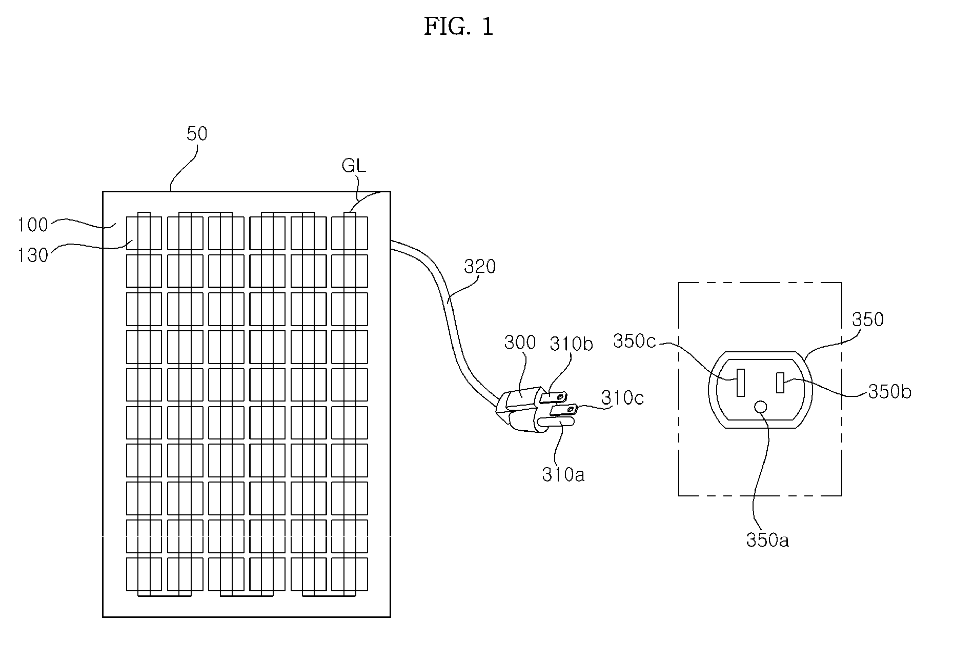
This application claims the priority benefit of Korean Patent Applications No. 10-2015-0104507, filed on Jul. 23, 2015 in the Korean Intellectual Property Office, the disclosure of which is incorporated herein by reference. Field of the Invention Embodiments of the present invention relate to a photovoltaic module and a photovoltaic system including the same, and more particularly, to a photovoltaic module and a photovoltaic system including the same, which may directly supply an Alternating Current (AC) voltage from the photovoltaic module to an outlet inside or outside a building. Description of the Related Art In recent years, due to depletion of existing energy resources, such as petroleum and coal, interest in alternative sources of energy to replace the existing energy resources is increasing. Most of all, solar cells are popular next generation cells to convert sunlight into electrical energy using semiconductor devices. Meanwhile, a photovoltaic module is defined by series or parallel connection of solar cells for photovoltaic power generation. The photovoltaic module may include a junction box for gathering electricity generated by the solar cells. It is an object of the embodiments of the present invention to provide a photovoltaic module and a photovoltaic system including the same, which may directly supply an Alternating Current (AC) voltage from the photovoltaic module to an outlet inside or outside a building. In accordance with one aspect of the present invention, the above and other objects can be accomplished by the provision of a photovoltaic module including a solar cell module, a converter to convert a direct current (DC) voltage from the solar cell module, an inverter to convert the DC voltage from the converter into an alternating current (AC) voltage, and a plug to outwardly output the AC voltage from the inverter, the plug having a ground terminal, wherein the ground terminal is electrically connected to a ground of the inverter, and wherein the ground of the inverter is electrically connected to a ground of the solar cell module. In accordance with another aspect of the present invention, there is provided a photovoltaic system including a plurality of photovoltaic modules each including a plug provided with a ground terminal, a connector connected to each plug of the photovoltaic modules, and an integration plug connected to the connector and provided with a ground terminal, wherein each of the photovoltaic modules includes a solar cell module, a converter to convert a DC voltage from the solar cell module, an inverter to convert the DC voltage from the converter into an AC voltage, and the plug to outwardly output the AC voltage from the inverter, the plug being provided with the ground terminal, wherein the ground terminal in each plug of the photovoltaic modules is electrically connected to a ground of the inverter, and wherein the ground of the inverter is electrically connected to a ground of the solar cell module. In accordance with a further aspect of the present invention, there is provided a photovoltaic system including a plurality of photovoltaic modules each including a plug provided with a ground terminal, a first connector connected to a first plug of a first photovoltaic module among the photovoltaic modules, a first connector plug connected to the first connector and provided with a ground terminal, a second connector connected to the first connector plug and connected to a second plug of a second photovoltaic module among the photovoltaic modules, and a second connector plug connected to the second connector and provided with a ground terminal, wherein each of the photovoltaic modules includes a solar cell module, a converter to convert a DC voltage from the solar cell module, an inverter to convert the DC voltage from the converter into an AC voltage, and the plug to outwardly output the AC voltage from the inverter, the plug being provided with the ground terminal, wherein the ground terminal in each plug of the photovoltaic modules is electrically connected to a ground of the inverter, and wherein the ground of the inverter is electrically connected to a ground of the solar cell module. The above and other objects, features and other advantages of the embodiments of the present invention will be more clearly understood from the following detailed description taken in conjunction with the accompanying drawings, in which: Hereinafter, the embodiments of the present invention will be described in detail with reference to the accompanying drawings. With respect to constituent elements used in the following description, suffixes “module” and “unit” are given or mingled with each other only in consideration of ease in the preparation of the specification, and do not have or serve as different meanings. Accordingly, the suffixes “module” and “unit” may be mingled with each other. Referring to First, the solar cell module 100 may include a plurality of solar cells 130. The solar cells 130 are semiconductor devices that convert solar energy into electrical energy, and may be, for example, silicon solar cells, compound semiconductor solar cells, tandem solar cells, dye sensitized solar cells, or CdTe or CIGS type solar cells. The respective solar cells 130 may be electrically connected in series, in parallel, or in series-parallel combination to one another. Although Meanwhile, a ground line GL of the solar cell module 100 may be electrically connected to any one string, among the strings, for ground connection to carry a Direct Current (DC) voltage from the solar cells 130. The ground line GL of the solar cell module 100 may be electrically connected to a frame 105 of the solar cell module 100, which is formed as a conductive member. Meanwhile, the photovoltaic module 50 according to the embodiment of the present invention includes the solar cell module 100, a converter unit (or converter) 530 for converting a DC voltage from the solar cell module 100, an inverter 540 for converting the DC voltage from the converter unit 530 into an AC voltage, and a plug 300 for outwardly outputting the AC voltage from the inverter 540, the plug 300 having a ground terminal 310 In particular, the photovoltaic module 50 may further include an AC power cable 320 between the inverter 540 and the plug 300. The AC power cable 320 includes three conductive lines. As illustrated in The first power line 320 Here, the first power terminal 310 Meanwhile, the plug 300, which includes the first power terminal 310 With this method of the embodiment of the present invention, a separate device for connecting the photovoltaic module 50 and the outlet 350 to each other is not necessary, resulting in improved user convenience. In particular, it is possible to allow a purchaser of the photovoltaic module 50 to install the photovoltaic module 50 inside a building and to connect the photovoltaic module 50 to the outlet 350 using the plug 300 in a simplified manner without any help from a service provider. Meanwhile, in the photovoltaic module 50 according to the embodiment of the present invention, a ground terminal 541 of the inverter 540 and the ground terminal 310 Accordingly, it is unnecessary to provide a separate ground to be connected to the ground terminal 541 of the inverter 540, which is advantageous. Meanwhile, referring to In addition, the frame 201 of the junction box 200 may be electrically connected to the frame 105 of the solar cell module 100 via a conductive member 305. Through this connection, the ground line GL of the solar cell module 100 is electrically connected to the ground terminal 310 Accordingly, it is unnecessary to provide a separate ground to be connected to the ground line GL of the solar cell module 100, which is advantageous. Meanwhile, the junction box 200 may include a bypass diode unit 510, the converter unit 530, a capacitor C1, the inverter 540, and a controller 550. This will be described below with reference to Referring to In Meanwhile, the second interface unit may sum an AC voltage from the first interface unit with an AC voltage from the second photovoltaic module 50 Meanwhile, an end of the second cable 330 Meanwhile, an end of the nth cable 320 may be connected to the plug 300, and the plug 300 may be electrically connected to the outlet 350. Referring to The first interface unit 342 Meanwhile, a cable 90 The second interface unit 342 To this end, the second interface unit 342 That is, one end of the cable 38 Referring to In addition, the photovoltaic system 500 of The connector 360 may be provided with connectors 360 Meanwhile, an AC power cable 365 may be provided between the connector 360 and the integration plug 368. The connector 360 may be provided with a first connector terminal, a second connector terminal, and a third connector terminal for electrical connection with a first power terminal, a second power terminal, and a ground terminal provided in each of the plugs 300 In addition, the first connector terminal, the second connector terminal, and the third connector terminal of the connector 360 are connected to one another in parallel, and consequently, sum AC voltages input through the respective plugs 300 Through the connector 360 and the integration plug 368, an AC voltage generated in the photovoltaic modules 50 Referring to In addition, the photovoltaic system 600 of The first connector 370 Meanwhile, one end of the first connector 370 The second connector 370 Meanwhile, one end of the second connector 370 The third connector 370 Meanwhile, one end of the third connector 370 Through the connectors 370 Referring to First, the solar cells 130 are semiconductor devices that convert solar energy into electrical energy, and may be, for example, silicon solar cells, compound semiconductor solar cells, tandem solar cells, dye sensitized solar cells, or CdTe or CIGS type solar cells. Each of the solar cells 130 includes a light-receiving surface on which sunlight is incident and a back surface opposite to the light-receiving surface. For example, the solar cell 130 may include a first conductive silicon substrate, a second conductive semiconductor layer formed on the silicon substrate, the second conductive type being contrary to the first conductive type, an anti-reflection film formed on the second conductive semiconductor layer and having at least one opening for exposing a surface portion of the second conductive semiconductor layer, a front electrode formed in contact with the surface portion of the second conductive semiconductor layer exposed through the opening, and a back electrode formed on the back surface of the silicon substrate. The respective solar cells 130 may be electrically connected in series, in parallel, or in series-parallel combination to one another. Specifically, the solar cells 130 may be electrically connected to one another using a ribbon 133. The ribbon 133 may be bonded to the front electrode formed on the light-receiving surface of one solar cell 130 and the back electrode formed on the back surface of another neighboring solar cell 130. The back substrate 110 may be a back sheet having waterproof, insulation, and ultraviolet (UV) blocking functions, and may be of a Tedlar/PET/Tedlar (TPT) type, without being limited thereto. In addition, while the back substrate 110 is illustrated in Meanwhile, the first sealing member 120 may be attached to the back substrate 110 so as to have the same size as the back substrate 110, and the solar cells 130 may be arranged next to one another so as to form a plurality of lines on the first sealing member 120. The second sealing member 150 may be disposed over the solar cells 130 and may be bonded to the first sealing member 120 via lamination. Here, the first sealing member 120 and the second sealing member 150 enable a chemical bond of respective elements of the solar cells 130. The first sealing member 120 and the second sealing member 150 may be formed of any one of various materials, such as ethylene vinyl acetate (EVA) films. Meanwhile, the front substrate 160 may be disposed on the second sealing member 150 so as to permit passage of sunlight therethrough. The front substrate 160 may be formed of tempered glass in order to protect the solar cells 130 from external shocks, etc. In addition, in order to prevent or reduce reflection of sunlight and to enhance light-transmittance, the front substrate 160 may be formed of low-iron tempered glass. Referring to For example, when a voltage of approximately 0.6 V is generated from a normal solar cell, the potential of a cathode of the first bypass diode Da is greater than the potential of an anode by approximately 12 V (=0.6 V*20). That is, the first bypass diode Da performs a normal operation rather than performing a bypassing operation. On the other hand, when a hot spot occurs at any one solar cell of the first solar cell string 140 Next, the second bypass diode Db is connected between the first bus ribbon 145 Next, the third bypass diode Dc is connected between the six solar cell string 140 Meanwhile, unlike Alternatively, the respective solar cell strings may be electrically connected to one another using bus ribbons. Meanwhile, the ribbon connected to the first string 140 Meanwhile, the junction box 200 may be located closer to one end of the solar cell module 100 from which the conductive lines extend. Referring to The bypass diode unit 510 may include the bypass diodes Dc, Db and Da located respectively between the first to fourth conductive lines 135 The bypass diodes Dc, Db and Da receive a photovoltaic DC voltage from the solar cell module 100, more particularly, from the first to fourth conductive lines 135 Meanwhile, an input voltage Vpv, having passed through the bypass diode unit 510, is input to the converter unit 530. The converter unit 530 converts the input voltage Vpv from the bypass diode unit 510. For this reason, the converter unit 530 may be referred to as a first power conversion unit. In one example, the converter unit 530 may convert a DC input voltage Vpv into a pseudo DC voltage. As such, the pseudo DC voltage may be stored in the capacitor C1. Both terminals of the capacitor C1 may be referred to as DC terminals, and the capacitor C1 may be referred to as a DC terminal capacitor. In another example, the converter unit 530 may boost the DC input voltage Vpv to convert the same into a boosted DC voltage. As such, the boosted DC voltage may be stored in the DC terminal capacitor C1. The inverter 540 may convert the DC voltage stored in the DC terminal capacitor C1 into an AC voltage. For this reason, the inverter 540 may be referred to as a second power conversion unit. In one example, the inverter 540 may convert the pseudo DC voltage from the converter unit 530 into an AC voltage. In another example, the inverter 540 may convert the boosted DC voltage from the converter unit 530 into an AC voltage. The converter unit 530 may include a plurality of interleaving converters for pseudo DC voltage conversion or boosted DC voltage conversion. In particular, the embodiment of the present invention assumes that the converter unit 530 including three or more interleaving converters. Current by the DC input voltage Vpv is reduced to 1/N in the n converters 610 Meanwhile, the n converters 610 When the n converters perform an interleaving operation as described above, a ripple of input current and output current of the converter unit 530 is reduced, which advantageously results in a reduction in the capacity and size of circuit elements in the power conversion module 700. In this way, the thickness of the junction box 200 may be reduced compared to the thickness of the frame 105 of the solar cell module 100. Meanwhile, the interleaving converters may be, for example, tapped inductor converters or flyback converters. The bypass diode unit 510 includes the first to third bypass diodes Da, Db and Dc, which are arranged respectively between an “a” node, a “b” node, a “c” node, and a “d” node, which respectively correspond to the first to fourth conductive lines 135 The converter unit 530 may perform power conversion using a DC voltage Vpv output from the bypass diode unit 510. In particular, each of the first to third tapped inductor converters 611 Among these tapped inductor converters, the first tapped inductor converter 611 Specifically, the switching element S1 may be connected between a tap of the tapped inductor T1 and the ground terminal. In addition, the output terminal (secondary side) of the tapped inductor T is connected to an anode of the diode D1, and the DC terminal capacitor C1 is connected between the cathode of the diode D1 and the ground terminal. Meanwhile, the primary side and the secondary side of the tapped inductor T1 have opposite polarities. The tapped inductor T1 may be referred to as a switching transformer. Meanwhile, the primary side and the secondary side of the tapped inductor T1 are connected to each other as illustrated in Meanwhile, when the three tapped inductor converters 611 Meanwhile, the respective tapped inductor converters 611 For example, the first tapped inductor converter 611 The inverter 540 converts a level-converted DC voltage from the converter unit 530 into an AC voltage. The inverter 540 is illustrated as a full-bridge inverter in The switching elements inside the inverter 540 are turned on/off based on an inverter switching control signal from the controller 550. As such, an AC voltage having a prescribed frequency is output from the inverter 540. The output AC voltage may have the same AC frequency (ranging from approximately 60 Hz to approximately 50 Hz) as the AC frequency of a grid. A filter unit 560 performs low-pass filtering in order to smooth the AC voltage output from the inverter 540. To this end, although the filter unit 560 is illustrated in Meanwhile, a converter input current detector A detects input current ic1 to the converter unit 530, and a converter input voltage detector B detects an input voltage vc1 to the converter unit 530. The detected input current ic1 and input voltage vc1 may be input to the controller 550. Meanwhile, a converter output current detector C detects output current ic2 from the converter unit 530, namely, DC-terminal current, and a converter output voltage detector D detects an output voltage vc2 from the converter unit 530, namely a DC-terminal voltage. The detected output current ic2 and output voltage vc2 may be input to the controller 550. Meanwhile, an inverter output current detector E detects output current ic3 from the inverter 540, and an inverter output voltage detector F detects an output voltage vc3 from the inverter 540. The detected current ic3 and voltage vc3 may be input to the controller 550. Meanwhile, the controller 550 may output a control signal to control the switching element S1 in the converter unit 530 illustrated in Meanwhile, the controller 550 may output an inverter control signal to control each of the switching elements Sa, S′a, Sb and S′b in the inverter 540. In particular, the controller 550 may output a turn-on timing signal for each of the switching elements Sa, S′a, Sb and S′b in the inverter 540 based on at least one of the detected input current ic1, input voltage vc1, output current ic2, output voltage vc2, output current ic3, and output voltage vc3. Meanwhile, the controller 550 may calculate the maximum power point of the solar cell module 100, and may control the converter unit 530 so as to output a DC voltage corresponding to the maximum power. Meanwhile, the ground terminal 541 of the inverter 540 is electrically connected to the ground line 320 In the same manner as in the power conversion module 700 of However, In particular, the first to third flyback converters 612 Among these flyback converters, the first flyback converter 612 Meanwhile, the ground terminal 541 of the inverter 540 is electrically connected to the ground line 320 Referring to Specifically, the converter unit 530 outputs a pseudo DC voltage, having a peak value of approximately 330 V, using a DC voltage, which ranges from approximately 32V to approximately 36V, from the solar cell module 100. To this end, the controller 550 determines duties of the switching elements in the first to third interleaving converters 610 In particular, as the input voltage Vpv is reduced, the duties of the switching elements in the first to third interleaving converters 610 Meanwhile, as the target output voltage Vdc is reduced, the duties of the switching elements in the first to third interleaving converters 610 Meanwhile, in order to allow a pseudo DC voltage waveform Vslo to more accurately follow a full-wave rectified waveform V sin, the embodiment of the present invention assumes that the switching frequency of the converter unit 530 is variable. As illustrated in In order to reduce the above-described error, in the embodiment of the present invention, the switching frequency of the converter unit 530 is varied. That is, the switching frequencies of the switching elements in the first to third interleaving converters 610 The controller 550 may control the converter unit 530 in such a manner that the switching frequency of the converter unit 530 is increased as the rate of variation of the target sinusoidal waveform V sin increases, and that the switching frequency of the converter unit 530 is reduced, as the rate of variation of the target sinusoidal waveform V sin is reduced. Meanwhile, variation in the switching frequency of First, (a) of Meanwhile, (a) of When the switching period of the interleaving converter is fixed and the DCM is applied as the switching mode, a waveform Idcm of current flowing through the switching element may be exemplified as illustrated in (b) of (c) of Meanwhile, a resonance section 1105 in the interleaving converter may occur after the switching element is turned off and before a next switching period is commenced. At this time, when the switching element is operated in the DCM, a section 1107 in which a switching voltage at both terminals of the switching element does not become zero occurs. Accordingly, zero voltage switching (ZVS) with respect to the switching element cannot be performed, which causes deterioration in the efficiency of the interleaving converter. To solve the above-described problem, in the embodiment of the present invention, a critical conduction mode (CRM), rather than the DCM, is used as the switching mode. The CRM may be referred to as a boundary conduction mode (BCM) or a transition mode (TM). The CRM refers to a mode in which a new switching period is commenced whenever current flowing through the switching element becomes zero after the switching element of the interleaving converter is turned off. As such, through the CRM method, the switching period may be varied according to the duty within the switching period. (a) of Meanwhile, (a) of When the CRM using a variable switching frequency is applied as the switching mode, the waveform Icrm of current flowing through the switching element may be exemplified as illustrated in (b) of (c) of Meanwhile, the resonance section 1105 in the interleaving converter may occur after the switching element is turned off. At this time, when the switching element is operated in the CRM, despite occurrence of the resonance section 1105 and 1109, a timing when current flowing through the switching element becomes zero may be determined, and the switching element may be turned on at the timing when the zero crossing arrives. That is, a new switching period may be commended. In this way, zero voltage switching (ZVS) with respect to the switching element may be performed, which enhances the efficiency of the interleaving converter. In this way, in the embodiment of the present invention, the switching frequency of the switching element in the interleaving converter is varied based on the CRM. Meanwhile, when the three interleaving converters 610 At this time, in the instance where a constant phase difference, e.g., 120 degrees, is set with respect to operating sections of the first to third interleaving converters 610 Referring to As illustrated, the switching periods of the three interleaving converters 610 At this time, the phase differences between the first interleaving converter to the third interleaving converter 610 In switching period variation sections 1310 and 1320 as described above, power output by each of the second interleaving converter and the third interleaving converter is reduced compared to the first interleaving converter. Thus, output current or output voltage of the converter unit 530 is instantaneously deteriorated. To solve this problem, in the embodiment of the present invention, when the switching periods of the interleaving converters are varied, phases of the operating sections of the interleaving converters are varied in order to avoid output unbalance between the interleaving converters. This will be described below with reference to Referring to As illustrated, the switching periods of the three interleaving converters 610 That is, unlike The controller 550 may vary the phases of the first to third interleaving converters 610 Meanwhile, the controller 550 may vary the phases of the first to third interleaving converters 610 Meanwhile, after the switching periods are varied, at the point in time of 18 Tv, the first interleaving converter is operated during a time section of 3 Tv after a time section of 9 Tv has passed from the previous switching period. On the other hand, the second interleaving converter may be operated during a time section of 3 Tv after a time section of 9.1 Tv has passed from the previous switching period, and the third interleaving converter may be operated during a time section of 3 TV after a time section of 9.1 Tv has passed from the previous switching period. After the switching periods of the three interleaving converters 610 As the phase differences between the first to third interleaving converters 610 Meanwhile, the phase variation as described above may be applied to the instance in which at least three interleaving converters are used. When two interleaving converters are used, phases of the interleaving converters may be fixed to 180 degrees as illustrated in Meanwhile, variation in the switching frequency and variation in the phase as described above with reference to The photovoltaic module and the photovoltaic system having the same according to the embodiment of the present invention may not be limitedly applied to the configuration and method of the embodiments as described above and, however, some or all of the embodiments may be selectively combined with one another to achieve various modifications. As is apparent from the above description, a photovoltaic module according to an embodiment of the present invention includes a solar cell module, a converter unit to convert a DC voltage from the solar cell module, an inverter to convert the DC voltage from the converter unit into an AC voltage, and a plug to outwardly output the AC voltage from the inverter, the plug having a ground terminal electrically connected to a ground of the inverter, which is electrically connected to a ground of the solar cell module. With this configuration, the AC voltage from the solar cell module may be directly supplied to an outlet inside or outside a building. Meanwhile, in order to electrically connect the ground of the solar cell module and a ground of a junction box including the inverter to each other, a conductive member is provided between a frame of the solar cell module and a frame of the junction box so as to interconnect the same. Thereby, a person who installs the photovoltaic module does not need to provide a ground for the solar cell module, which ensures ease of installation. Meanwhile, the photovoltaic module includes a first interface unit to receive an AC voltage from an adjacent photovoltaic module, and a second interface unit to output the AC voltage from the first interface unit and the AC voltage from the inverter to the plug, whereby AC voltages from a plurality of photovoltaic may be directly supplied to the outlet inside or outside the building via the single plug. Meanwhile, a plurality of interleaving converters performs an interleaving operation, which may reduce a ripple of input current and output current of the converter unit. Accordingly, the capacity and size of switching elements inside the converter unit or the inverter may be advantageously reduced. In the photovoltaic module, a junction box including the converter unit and the inverter may be attached to the back surface of the solar cell module. As such, the photovoltaic module may directly output the AC voltage in a stabilized manner. A photovoltaic system according to an embodiment of the present invention includes a plurality of photovoltaic modules each including a plug provided with a ground terminal, a connector connected to each plug of the photovoltaic modules, and an integration plug connected to the connector and including a ground terminal, and each of the photovoltaic modules includes a solar cell module, a converter unit to convert a DC voltage from the solar cell module, an inverter to convert the DC voltage from the converter unit into an AC voltage, and the plug to outwardly output the AC voltage from the inverter, the plug being provided with the ground terminal. The ground terminal in each plug of the photovoltaic modules is electrically connected to a ground of the inverter, and the ground of the inverter is electrically connected to a ground of the solar cell module. In this way, AC voltages from the photovoltaic modules may be directly supplied to an outlet inside or outside a building using the connector and the integration plug. A photovoltaic system according to an embodiment of the present invention includes a plurality of photovoltaic modules each including a plug provided with a ground terminal, a first connector connected to a first plug of a first photovoltaic module among the photovoltaic modules, a first connector plug connected to the first connector and having a ground terminal, a second connector connected to the first connector plug and connected to a second plug of a second photovoltaic module among the photovoltaic modules, and a second connector plug connected to the second connector and having a ground terminal, and each of the photovoltaic modules includes a solar cell module, a converter unit to convert a DC voltage from the solar cell module, an inverter to convert the DC voltage from the converter unit into an AC voltage, and the plug to outwardly output the AC voltage from the inverter, the plug being provided with the ground terminal. The ground terminal in each plug of the photovoltaic modules is electrically connected to a ground of the inverter, and the ground of the inverter is electrically connected to a ground of the solar cell module. In this way, AC voltages from the photovoltaic modules may be directly supplied to an outlet inside or outside a building using the first connector, the first connector plug, the second connector, and the second connector plug. Although the embodiments of the present invention have been disclosed for illustrative purposes, those skilled in the art will appreciate that the present invention is not limited to the above-described embodiments and various modifications are possible without departing from the scope and spirit of the invention as disclosed in the accompanying claims. These modifications should not be understood separately from the idea or outlook of the present invention. Disclosed are a photovoltaic module and a photovoltaic system including the same. The photovoltaic module includes a solar cell module, a converter to convert a DC voltage from the solar cell module, an inverter to convert the DC voltage from the converter into an AC voltage, and a plug to outwardly output the AC voltage from the inverter, the plug having a ground terminal. The ground terminal is electrically connected to a ground of the inverter, and the ground of the inverter is electrically connected to a ground of the solar cell module. Thereby, the AC voltage from the photovoltaic module is directly supplied to an outlet inside or outside a building. 1. A photovoltaic module comprising:
a solar cell module; a converter to convert a direct current (DC) voltage from the solar cell module; an inverter to convert the DC voltage from the converter into an alternating current (AC) voltage; and a plug to outwardly output the AC voltage from the inverter, the plug having a ground terminal, wherein the ground terminal is electrically connected to a ground of the inverter, and wherein the ground of the inverter is electrically connected to a ground of the solar cell module. 2. The photovoltaic module according to 3. The photovoltaic module according to 4. The photovoltaic module according to 5. The photovoltaic module according to a first interface unit to receive an AC voltage from an adjacent photovoltaic module; and a second interface unit to output the AC voltage from the first interface unit and the AC voltage from the inverter to the plug. 6. The photovoltaic module according to wherein the converter includes a plurality of interleaving converters. 7. The photovoltaic module according to 8. The photovoltaic module according to wherein the controller varies a switching period for switching elements of the interleaving converters based on a duty for driving the switching elements of the interleaving converters. 9. The photovoltaic module according to 10. The photovoltaic module according to 11. A photovoltaic system comprising:
a plurality of photovoltaic modules each including a plug provided with a ground terminal; a connector connected to each plug of the photovoltaic modules; and an integration plug connected to the connector and provided with a ground terminal, wherein each of the photovoltaic modules includes: a solar cell module; a converter to convert a DC voltage from the solar cell module; an inverter to convert the DC voltage from the converter into an AC voltage; and the plug to outwardly output the AC voltage from the inverter, the plug being provided with the ground terminal, wherein the ground terminal in each plug of the photovoltaic modules is electrically connected to a ground of the inverter, and wherein the ground of the inverter is electrically connected to a ground of the solar cell module. 12. The photovoltaic system according to 13. The photovoltaic system according to 14. The photovoltaic system according to a first interface unit to receive an AC voltage from an adjacent photovoltaic module; and a second interface unit to output the AC voltage from the first interface unit and the AC voltage from the inverter to the plug. 15. A photovoltaic system comprising:
a plurality of photovoltaic modules each including a plug provided with a ground terminal; a first connector connected to a first plug of a first photovoltaic module among the photovoltaic modules; a first connector plug connected to the first connector and provided with a ground terminal; a second connector connected to the first connector plug and connected to a second plug of a second photovoltaic module among the photovoltaic modules; and a second connector plug connected to the second connector and provided with a ground terminal, wherein each of the photovoltaic modules includes: a solar cell module; a converter to convert a DC voltage from the solar cell module; an inverter to convert the DC voltage from the converter into an AC voltage; and the plug to outwardly output the AC voltage from the inverter, the plug being provided with the ground terminal, wherein the ground terminal in each plug of the photovoltaic modules is electrically connected to a ground of the inverter, and wherein the ground of the inverter is electrically connected to a ground of the solar cell module. 16. The photovoltaic system according to a third connector connected to the second connector plug and connected to a third plug of a third photovoltaic module among the photovoltaic modules; and a final plug connected to the third connector and provided with a ground terminal; 17. The photovoltaic system according to 18. The photovoltaic system according to 19. The photovoltaic system according to a first interface unit to receive an AC voltage from an adjacent photovoltaic module; and a second interface unit to output the AC voltage from the first interface unit and the AC voltage from the inverter to the plug.CROSS-REFERENCE TO RELATED APPLICATION
BACKGROUND OF THE INVENTION
SUMMARY OF THE INVENTION
BRIEF DESCRIPTION OF THE DRAWINGS
DETAILED DESCRIPTION OF THE EMBODIMENTS