LIQUID CRYSTAL DISPLAY
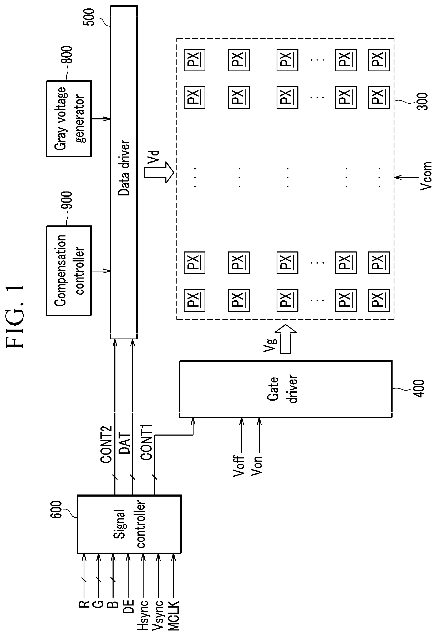
This application is a continuation application of U.S. patent application Ser. No. 15/098,044 filed on Apr. 13, 2016, which claims priority to and the benefit of Korean Patent Application No. 10-2015-0060003 filed in the Korean Intellectual Property Office on Apr. 28, 2015, the entire contents of which are incorporated herein by reference. The present inventive concept relates to a liquid crystal display. Liquid crystal displays, which are one of the most common types of flat panel displays currently in use, include two sheets of array panels with field generating electrodes, such as a pixel electrode, a common electrode, and the like, and a liquid crystal layer interposed therebetween, and the liquid crystal display generates an electric field in the liquid crystal layer by applying a voltage to the field generating electrodes to determine alignment of liquid crystal molecules in the liquid crystal layer through the generated electric field and to control polarization of incident light, thereby displaying images. Among the liquid crystal displays, a vertically aligned mode liquid crystal display, in which liquid crystal molecules are aligned so that long axes thereof are perpendicular to the upper and lower panels when no electric field is applied, has gained attention because its contrast ratio is large and a wide reference viewing angle is easily implemented. In such a vertically aligned mode liquid crystal display, in order to implement a wide viewing angle, a plurality of domains having different alignment directions for the liquid crystal molecules may be formed in one pixel. As such, as a means of forming the plurality of domains, a method of forming cutouts such as slits in the field generating electrode is used as a domain division means. According to the method, the plurality of domains may be formed by realigning the liquid crystal molecules in a fringe field formed between edges of the cutouts and the field generating electrodes facing the edges. When the domain division means, such as cutouts, are formed in the field generating electrode, misalignment may occur between field generating electrodes that face each other, and thus a distance between domain division means may be changed, thereby causing the response speed of liquid crystal molecules in the domains to be changed. When the response speed of the liquid crystal molecules is changed according to a location of the domain, the display quality of the display may be deteriorated. The above information disclosed in this Background section is only to enhance the understanding of the background of the inventive concept and therefore it may contain information that does not form the prior art that is already known in this country to a person of ordinary skill in the art. The present inventive concept has been made in an effort to provide a liquid crystal display that can prevent the deterioration of display quality by preventing liquid crystal molecules from being irregularly moved and the reduction of response speed according to a location in the liquid crystal display including a plurality of domains. A liquid crystal display according to an exemplary embodiment of the present inventive concept includes: a plurality of pixels including a plurality of pixel electrodes formed on a first substrate and including first domain division means, and a common electrode formed on a second substrate that faces the first substrate and including second domain division means; a gate driver and a data driver connected to the plurality of pixels; and a compensation controller connected to the data driver, the compensation controller transmits compensation voltages to the data driver, wherein, when viewed on the same plane, distances between the first domain division means and the second domain division means are changed according to a location of the plurality of pixels, and wherein the compensation voltages are changed corresponding to the distances between the first domain division means and the second domain division means. The liquid crystal display may be curved. The first domain division means of the pixel electrode may be a plurality of first cutouts formed in the pixel electrode, wherein the second domain division means of the common electrode are a plurality of second cutouts formed in the common electrode, and wherein the distances between the first domain division means and the second domain division means are a maximum distance between the plurality of first cutouts and the plurality of second cutouts. The plurality of pixel electrodes include plane portions having a plane shape and a plurality of branch electrodes extending from the plane portions, wherein the common electrode comprises cross-shaped cutouts overlapping the plane portions of the plurality of pixel electrode, and the distance between the first domain division means and the second domain division means is a maximum distance between a center portion of each of the cross-shaped cutouts of the common electrode and an edge of each of the plane portions of the pixel electrodes. The compensation voltages may be higher than target gray voltages of the plurality of pixels, and wherein, as the distances between the first domain division means and the second domain division means are increased, the compensation voltages are increased. As the distances between the first domain division means and the second domain division means may be increased by about 5 μm, magnitude of the compensation voltages may be increased by about 0.3V to about 0.4V. When the distances between the first domain division means and the second domain division means are about 20 μm, the magnitude of the compensation voltages are about 1.5V; when the distances between the first domain division means and the second domain division means are about 25 μm, the magnitude of the compensation voltages are about 1.8V to about 1.9V; when the distances between the first domain division means and the second domain division means are about 30 μm, the magnitude of the compensation voltages are about 2.1V to about 2.2V; and when the distances between the first domain division means and the second domain division means are about 35 μm, the magnitude of the compensation voltages are about 2.4V to about 2.5V. The compensation controller may include a compensation determiner that determines whether compensation is needed according to a location of the plurality of pixels and a lookup table that stores values of the compensation voltages. The compensation controller may include: a compensation determiner that determines whether compensation is needed according to a location of the plurality of pixels; a lookup table that stories values of the compensation voltage; and a compensation data calculator that receives at least two compensation voltages of at least two distances between the first domain division means and the second domain division means from the lookup table and calculates the compensation voltages corresponding to locations of the plurality of pixels using the received at least two compensation voltages. The compensation data calculator may compensation data calculator use a linear function to calculate the compensation voltages. The liquid crystal display may include a liquid crystal layer provided between the first substrate and the second substrate, wherein liquid crystal molecules of the liquid crystal layer are arranged to be substantially perpendicular to the surface of the first and second substrates when no electric field is applied to the liquid crystal layer. According to the exemplary embodiment of the present inventive concept, irregular movement and slow response speed of the liquid crystal molecules according to locations in the liquid crystal display can be prevented, thereby preventing deterioration of display quality. The present inventive concept will be described more fully hereinafter with reference to the accompanying drawings, in which exemplary embodiments of the inventive concept are shown. As those skilled in the art would realize, the described embodiments may be modified in various different ways, all without departing from the spirit or scope of the present inventive concept. In the drawings, the thickness of layers, films, panels, regions, etc., are exaggerated for clarity. Like reference numerals designate like elements throughout the specification. It will be understood that when an element such as a layer, film, region, or substrate is referred to as being “on” another element, it can be directly on the other element or intervening elements may also be present. In contrast, when an element is referred to as being “directly on” another element, there are no intervening elements present. First, a liquid crystal display according to an exemplary embodiment of the present inventive concept will be described in detail with reference to As shown in From the viewpoint of an equivalent circuit, the liquid crystal panel assembly 300 includes a plurality of signal lines GLa, GLb, DL, and CL (refer to Referring to The liquid crystal display assembly 300 according to the present exemplary embodiment includes a plurality of signal lines and the plurality of pixels PX connected to the signal lines. Each pixel PX includes a pair of subpixels, and each subpixel includes liquid crystal capacitors Clca and Clcb. The two subpixels include gate lines GLa and GLb, a data line DL, and switching elements Qa connected to the liquid crystal capacitor Clca, Qb connected to the liquid crystal capacitor Clcb, and Qc connected to the liquid crystal capacitor Clcb. However, according to another exemplary embodiment of the present inventive concept, each pixel may include one subpixel. The liquid crystal capacitors Clca and Clcb use subpixel electrodes PEa/PEb of the first display panel 100 and a common electrode CE of the second display panel 200 as two terminals, and the liquid crystal layer 3 provided between the subpixel electrodes PEa/PEb and the common electrode 270 functions as a dielectric material. The pair of subpixel electrodes PEa and PEb are separated from each other, and form one pixel electrode PE. The common electrode CE is formed on a front surface of the second display panel 200 and is applied with the common voltage Vcom. The liquid crystal layer 3 has negative dielectric anisotropy, and liquid crystal molecules of the liquid crystal layer 3 are aligned so that long axes thereof are perpendicular to the surfaces of the two panels 100 and 200 when no electric field is applied. Unlike in A polarizer (not shown) is provided on an outer surface of each of the display panels 100 and 200, and polarization axes of the two polarizers may cross each other perpendicularly. In the case of a reflective liquid crystal display, one of the two polarizers may be omitted. In case the polarizers are crossed polarizers, the light incident upon the liquid crystal layer 3 is blocked when no electric fields are applied thereto. Referring to The gate driver 400 is connected to the gate lines GLa and GLb of the liquid crystal panel assembly 300, and applies gate signals having a gate on voltage Von and a gate off voltage Voff to the gate lines GLa and GLb. The data driver 500 is connected to the data lines DL of the liquid crystal panel assembly 300, and selects gray voltages from the gray voltage generator 800 to apply them to the data lines DL as data voltages. However, in case the gray voltage generator 800 does not provide all of the gray voltages, but only a limited number of reference gray voltages, the data driver 500 divides the reference gray voltages to thereby generate the desired data voltages. The compensation controller 900 determines whether voltage compensation is required or not according to regions of the liquid crystal display, and supplies a compensation voltage to the data driver 500. The signal controller 600 controls the gate driver 400 and the data driver 500. Each of the circuit elements 400, 500, 600, 800, and 900 may be directly mounted on the liquid crystal display assembly 300. Each of the circuit elements 400, 500, 600, 800, and 900 may be mounted on the flexible printed circuit film as at least one IC chip, and may be attached to the liquid crystal display assembly 300 as a tape carrier package (TCP). Each of the circuit elements 400, 500, 600, 800, and 900 may be mounted on an additional printed circuit board (PCB) (not shown). Alternatively, the drivers 400, 500, 600, 800, and 900 may be integrated with the liquid crystal display assembly 300 together with the signal lines GLa, GLb, and DL and the thin film transistor switching elements Qa, Qb, and Qc. Further, the circuit elements 400, 500, 600, 800, and 900 can be integrated into a single IC chip, and at least one of them or at least one circuit element configuring them can be provided in another IC chip. Referring to Each pixel PX includes a first switching element Qa, a second switching element Qb, a third switching element Qc, a first liquid crystal capacitor Clca, a second liquid crystal capacitor Clcb, and a step-down capacitor Cstd. The first switching element Qa and the second switching element Qb are connected to the first gate line GLa and the data line DL, and the third switching element Qc is connected to the second gate line GL. The first switching element Qa and the second switching element Qb are three-terminal elements, such as thin film transistors provided in the first display panel 100, and each includes a control terminal connected to the first gate line GLa, an input terminal connected to the data line DL, and an output terminal connected to the first liquid crystal capacitor Clca and the second liquid crystal capacitor Clcb, respectively. The third switching element Qc is also a three-terminal element, such as a thin film transistor provided in the first display panel 100, and includes a control terminal connected to the second gate line GLb, an input terminal connected to the second liquid crystal capacitor Clcb, and an output terminal connected to the step-down capacitor Cstd. The step-down capacitor Cstd is connected between the output terminal of the third switching element Qc and the capacitor electrode line CL, and the capacitor electrode line CL provided in the first display panel 100 and an output electrode of the third switching element Qc overlap each other, with an insulator interposed therebetween. Referring to First, referring to The signal controller 600 processes the input image signals R, G, and B according to an operating condition of the liquid crystal display assembly 300 based on the input image signals R, G, and B, generates a gate control signal CONT1 and a data control signal CONT2, and transmits the gate control signal CONT1 to the gate driver 400 and the data control signal CONT2 and a processed image signal DAT to the data driver 500. The output image signal DAT is a digital signal and has a value of a predetermined number (or a gray). The data driver 500 receives the digital image signal DAT for the pixels PX of one row according to the data control signal CONT2 from the signal controller 600 and selects a gray voltage corresponding to each digital image signal DAT, such that the data driver 500 converts the digital image signal DAT to an analog data voltage and then applies the converted analog data voltage to the data line DL. In this case, the compensation controller 900 determines whether a compensation signal needs to be applied according to a location of the liquid crystal display, and supplies a compensation signal to the data driver 500. The gate driver 400 applies a gate-on voltage Von to the gate lines GLa and GLb according to the gate control signal CONT1 from the signal controller 600 to turn on the switching elements Qa, Qb, and Qc connected to the gate lines GLa and GLb. Then, the data voltage Vd applied to the data line DL is applied to the corresponding pixel PX through the first and second turn-on switching elements Qa and Qb. Next, a specific pixel row, for example, an i-th pixel row will be described in detail. A first gate signal is applied to a first gate line GLa of the i-th row and a second gate signal is applied to a second gate line GLb. When the first gate signal is changed to a gate-on voltage Von from a gate-off voltage Voff, the first and second switching elements Qa and Qb connected thereto are turned on. Accordingly, the data voltage Vd applied to the data line DL is applied to the first and second subpixel electrodes PEa and PEb through the first and second turn-on switching elements Qa and Qb. In this case, the data voltage Vd applied to the first subpixel electrode PEa and the data voltage Vd applied to the second subpixel electrode PEb are equivalent to each other. The first and second liquid crystal capacitors Clca and Clcb are charged by the same value as a difference between the common voltage Vcom and the data voltage Vd. Thereafter, when the first gate signal is changed to the gate-off voltage Voff from the gate-on voltage Von and the second gate signal is changed to the gate-on voltage Von from the gate-off voltage Voff, the first and second switching elements Qa and Qb are turned off and the third switching element Qc is turned on. Then, charges are moved to the third drain electrode 175 In this case, the charging voltages of the two liquid crystal capacitors Clca and Clcb represent different gamma curves, and a gamma curve of one pixel becomes a curve acquired by combining the different gamma curves. A combined gamma curve at the front coincides with a reference gamma curve at the front which is predetermined to be the most suitable, and a combined gamma curve at the side becomes closest to the reference gamma curve at the front. As such, side visibility is improved by converting image data into two image data which have two different gamma curves. The above-described process is repeated by a 1 horizontal period [also, referred to as “1H” and is the same as one cycle of the horizontal synchronizing signal Hsync and the data enable signal DE] as a unit, such that images of one frame are displayed by applying the data voltage Vd to all the pixels PX. The polarity of an inversion signal RVS applied to the data driver 500 is changed every frame so that polarity of the data voltage Vd applied to each pixel PX is opposite to polarity in the previous frame. The voltages charged at the first and second liquid crystal capacitors Csta and Cstb may be controlled according to the capacitance of the step-down capacitor Cstd. In the present exemplary embodiment, two subpixel electrodes are disposed in one pixel and thus two liquid crystal capacitors Clca and Clcb are included, but in a liquid crystal display according to another exemplary embodiment of the present inventive concept, one sub-pixel electrode is provided in one pixel so that one liquid crystal capacitor may be included. Next, a liquid crystal panel assembly according to an exemplary embodiment of the present inventive concept will be described with reference to The liquid crystal display according to the present exemplary embodiment includes a first display panel 100, a second display panel 200, and a liquid crystal layer 3 disposed between the two display panels 100 and 200. The first display panel 100 and the second display panel 200 are disposed facing each other. First, the first display panel 100 will be described. A plurality of gate conductors including a gate line 121 and a capacitor voltage line 131 are formed on a first substrate 110. The gate line 121 includes a first gate electrode 124 The capacitor voltage line 131 transmits a constant capacitor voltage, and includes a vertically expanded first capacitor electrode 137. A gate insulating layer 140 is formed on the gate conductors 121 and 131. A first semiconductor 154 The semiconductor 154 Ohmic contacts 163 A data conductor including a data line 171, first, second, and third source electrodes 173 The first gate electrode 124 A passivation layer 180 is formed on the data conductors 171, 173 A plurality of contact holes 185 A pixel electrode 191 including first and second subpixel electrodes 191 The first subpixel electrode 191 The first subpixel electrode 191 The first subpixel electrode 191 The first capacitor electrode 137 and the second capacitor electrode 177 overlap each other, interposing the gate insulating layer 140 therebetween such that the step-down capacitor Cstd is formed. As described, the step-down capacitor Cstd is formed using the gate conductor and the data conductor so that an additional process for forming the step-down capacitor Cstd is not required, thereby simplifying a manufacturing process of the liquid crystal display. A lower alignment layer (not shown) is formed on the pixel electrode 191 and the passivation layer 180. The lower alignment layer may be a vertical alignment layer. Next, the second display panel 200 will be described. A light blocking member 220 is formed on the second substrate 210. The light blocking member 220 is also referred to as a black matrix, and prevents light leakage. A plurality of color filters 230 are formed on a second substrate 210 in a region defined by the light blocking member 220. The color filters 230 may include one of the primary colors red, green, and blue, and may be formed of an organic material including a pigment displaying one of the three primary colors. In the present exemplary embodiment, the color filters 230 are formed on the second display panel 200, but color filters 230 may be formed on a first display panel 100 in a liquid crystal display according to another exemplary embodiment of the present inventive concept. Further, the light blocking member 220 is formed on the second display panel 200 in the present exemplary embodiment, and a light block member 220 may be formed on a first display panel 100 in a liquid crystal display according to another exemplary embodiment of the present inventive concept. An overcoat 250 is formed on the light blocking member 220 and the color filter 230. The common electrode 270 is formed on the overcoat 250. A plurality of second cutouts 71, 72, 73, 74 An upper alignment layer (not shown) is formed on the common electrode 270. The upper alignment layer may be a vertical alignment layer. The liquid crystal layer 3 has negative dielectric anisotropy, and liquid crystal molecules of the liquid crystal layer 3 are aligned so that long axes thereof are perpendicular to the surfaces of the two panels 100 and 200 while the electric field is not applied. When a common voltage is applied to the common electrode 270 and the data voltage is applied to the pixel electrode 191, an electric field substantially perpendicular to the surface of the display panels 100 and 200 is formed. Thus, liquid crystal molecules 31 of the liquid crystal layer 3 change directions so that the major axes thereof become perpendicular to the direction of the electric field in response to the electric field. Hereinafter, both the pixel electrode 191 and the common electrode 270 are commonly referred to as field generating electrodes. The cutouts 71, 72, 73, 74 Each of the cutout sets 71, 72, 73, 74 The plurality of first cutouts 9293 Next, features of a liquid crystal display according to an exemplary embodiment of the present inventive concept will be described with reference to Referring to As shown in Alignments between the first display panel 100 and the second display panel 200 may be different from each other according to locations of the liquid crystal display, as shown in As described, when the degree of misalignment of the liquid crystal display is changed, a distance between the first domain division means and the second domain division means formed in the pixel electrode and the common electrode may be changed. Next, operation of the liquid crystal display according to the present exemplary embodiment of the present inventive concept will be described with reference to Referring to Referring to A second fringe field FF2 is formed in the first region where the distance between the first domain division means 90 and the second domain division means 70 is relatively as narrow as the second distance d2, and a third fringe field FF3 is formed in the second region where the distance between the first domain division means 90 and the second domain division means 70 is the first distance d1. That is, when the strength of the fringe field is changed according to locations in the liquid crystal display, reaction of the liquid crystal molecules to the fringe field is also changed according to the locations. For example, a first liquid crystal molecule 31 Next, referring to Referring to The compensation determiner 900 When the compensation determiner 900 As previously described, when the liquid crystal display is curved, the degree of misalignment between the first display substrate 100 and the second display substrate 200 may be changed according to locations in the display panel, for example, the first region Ra, the second regions Rb, the third regions Rc, the fourth regions Rd, and the fifth regions Re may have different misalignment degrees. Thus, the compensation determiner 900 Once the compensation determiner 900 The magnitude of the compensation voltage V2 may be changed depending on a distance between the first domain division means 90 and the second domain division means 70 of the pixel electrode 191. Compared to the case in which no misalignment occurs, the compensation voltage V2 may be increased by from about 0.3V to about 0.4V as the first distance d1 between the first domain division means 90 and the second domain division means 70 is increased by about 5 μm. More specifically, when the distance between the first domain division means 90 and the second domain division means 70 is about 20 μm, the magnitude of the input compensation voltage V2 is about 1.5V; when the first distance d1 between the first domain division means 90 and the second domain division means 70 is increased by about 5 μm, the magnitude of the compensation voltage V2 applied to a pixel located in a region of 25 μm may be from about 1.8V to about 1.9V; when the first distance d1 between the first domain division means 90 and the second domain division means 70 is increased by about 10 μm, the magnitude of the compensation voltage V2 applied to a pixel located in a region of about 30 μm may be from about 2.1V to about 2.2V; and when the first distance d1 between the first domain division means 90 and the second domain division means 70 is increased by about 15 μm, the magnitude of the compensation voltage V2 applied to a pixel located in a region of 35 μm may be from about 2.4V to about 2.5V. Next, an experimental example of the present inventive concept will be described with reference to In the present experimental example, distances between the first domain division means 90 and the second domain division means 70 are respectively set to be about 23 μm, about 28 μm, and about 34 μm, and response speed (response time) according to the compensation voltage V applied to a pixel is measured and shown in the graph. First, referring to Referring to As such, the magnitude of the compensation voltage V2 input by the compensation controller 900 of the liquid crystal display according to the exemplary embodiment of the present inventive concept may be about 1.5V in the case of a pixel located in a region where a first distance d1 between the first domain division means 90 and the second domain division means 70 is about 20 μm, may be about 1.8V to about 1.9V in the case in which a pixel of which a distance between the first domain division means 90 and the second domain division means 70 is about 25 μm, may be about 2.1V to about 2.2V in the case in which a pixel located in a region where the first distance d2 between the first domain division means 90 and the second domain division means 70 is about 30 μm, and may be about 2.4V to about 2.5V in the case in which a pixel located in a region where the first distance d1 between the first domain division means 90 and the second domain division means 70 is about 35 μm. When the compensation voltage V2 is applied by the compensation controller 900 of the liquid crystal display according to the exemplary embodiment of the present inventive concept, response speed may be equal to or shorter than about 25 μms, which is response time generally required in a vertical alignment liquid crystal display. An operation of a compensation controller 900 of a liquid crystal display according to another exemplary embodiment of the present inventive concept will be described with reference to Referring to The compensation determiner 900 When the compensation determiner 900 The compensation controller 900 of the liquid crystal display according to the exemplary embodiment of The calculator 900 Accordingly, in such a calculation, the magnitude of an input compensation voltage can be determined even though a distance between the first domain division means 90 and the second domain division means 70 has a value that is not stored in the lookup table 900 The magnitude of a compensation voltage stored in the lookup table 900 Next, a liquid crystal display according to another exemplary embodiment of the present inventive concept will be described with reference to Referring to First, the first display panel 100 will be described. A plurality of gate conductors including a gate line 121 The capacitor voltage line 131 transmits a predetermined capacity voltage, and includes a first capacity electrode 137 expanded downward. A gate insulating layer 140 is formed above the gate conductors 121 The semiconductor 154 A data conductor including a data line 171, first, second, and third source electrodes 173 The first gate electrode 124 A passivation layer 180 is formed on the data conductors 171, 173 A plurality of contact holes 185 A pixel electrode 191 The first subpixel electrode 191 The first subpixel electrode 191 The branch electrodes 194 each include a portion that obliquely extending in a top right direction, a portion that obliquely extending in a bottom right direction, a portion that obliquely extending in a top left direction, and a portion that obliquely extending in a bottom left direction. As described, the directions in which the liquid crystal molecules of the liquid crystal layer 3 are inclined become different at the portions where the directions in which the branch electrodes 194 extend are different. Hence, four domains with different directions in which the liquid crystal molecules are inclined are formed on the liquid crystal layer 3. When the directions in which the liquid crystal molecules are inclined are varied, a reference viewing angle of the liquid crystal display is increased. The first gate electrode 124 Next, the upper display panel 200 will be described. A light blocking member 220 is provided on a second substrate 210. The light blocking member 220 which is called as a black matrix blocks light leakage. A plurality of color filters 230 are provided on the second substrate 210 and the light blocking member 220. An overcoat 250 is provided on the color filters 230. The overcoat 250 prevents the color filters 230 and the light blocking member 220 from being lifted, and prevents contamination of the liquid crystal layer 3 from organic materials, such as a solvent included in the color filters 230, defect such as an afterimage that may be induced when a screen is driven. When circumstances require, the overcoat 250 can be omitted. A common electrode 270 is provided on the overcoat 250. The light blocking member 220 and the color filters 230 are provided on the second display panel 200 in the liquid crystal display according to the present exemplary embodiment, and the light blocking member 220 and the color filter 230 may be provided on the first display panel 100 in a liquid crystal display according to another exemplary embodiment of the present inventive concept. In this case, the color filters 230 may be provided instead of the passivation layer 180 of the first display panel 100. The common electrode 270 may include cross-shaped third cutouts 271 provided in locations respectively corresponding to basic regions of the first subpixel electrode 191 When the liquid crystal display is viewed from the top, sub-regions of the first subpixel electrode 191 The pixel electrodes 191 The liquid crystal layer 3 provided between the two display panels 100 and 200 includes a plurality of liquid crystal molecules having negative dielectric anisotropy. The liquid crystal molecules may be aligned so that long axes thereof are perpendicular with respect to the surfaces of the two display panels 100 and 200 in a state in which there is no electric field. The first subpixel electrode 191 An electric field is applied to the liquid crystal layer 3 by voltages applied to the first subpixel electrode 191 Next, the basic region of the pixel area of the liquid crystal display according to the present exemplary embodiment of the present inventive concept will be described with reference to Referring to The basic region includes a pixel electrode 191 including plane portion 193 having a plane shape such as a rhombus shape and a plurality of branch electrodes 194 respectively extending in four different directions from the plane portion 193, with third cutouts 271 of a common electrode 270 facing the pixel electrode 191. A center portion of the plane portion 193 of the pixel electrode 191 overlaps a center portion of the cross-shaped third cutout 271 formed in the common electrode 270. Each of the plurality of branch electrodes 194 of the pixel electrode 191 includes a portion that is obliquely extending in a top right direction, a portion that is obliquely extending in a bottom right direction, a portion that is obliquely extending in a top left direction, and a portion that is obliquely extending in a bottom left direction. As described above, the basic region of the field generating electrode is divided into four sub-regions by the plurality of branch electrodes 194 of the pixel electrode 191 and the cross-shaped third cutouts 271 of the common electrode 270. The tilting direction of a director of the liquid crystal molecules in each sub-region, more specifically, an azimuthal angle, which is a direction of a director of the liquid crystal molecules, is different from each other. The strength of a fringe field applied to the liquid crystal molecules, which causes the liquid crystal molecule to be tilted is changed according to a third distance d3 between a center portion of the cross-shaped third cutout 271 of the common electrode 270 and an edge of the plane portion 193 of the pixel electrode 191. When the third distance d3 between the center portion of the cross-shaped third cutout 271 of the common electrode 270 and the edge of the plane portion 193 of the pixel electrode 191 is decreased, the strength of the fringe field is increased, and when the third distance d3 is increased, the strength of the fringe field is decreased. Referring to That is, as the third distance d3 between the center portion of the cross-shaped third cutout 271 of the common electrode 270 and the edge of the plane portion 193 of the pixel electrode 191 is increased, the liquid crystal molecules are tilted relatively slowly when the liquid crystal is under biased and accordingly tilting directions may be irregular depending on the locations. When the tilting speed of the liquid crystal molecules is slow and tilting directions are irregular, the liquid crystal molecules irregularly move, and thus display quality of the display is deteriorated. The magnitude of a compensation voltage input to a data driver 500 from a compensation controller 900 of the liquid crystal display is changed according to the third distance d3 between the center portion of the cross-shaped third cutout 271 of the common electrode 270 and the edge of the plane portion 193 of the pixel electrode 191. Compared to the case in which no misalignment occurs, the magnitude of the compensation voltage V2 applied to a pixel located in a region where the third distance d3 between the center portion of the cross-shaped third cutout 271 of the common electrode 270 and the edge of the plane portion 193 of the pixel electrode 191 is about 25 μm may be about 1.8V to about 1.9V; the magnitude of the compensation voltage V2 applied to a pixel located in a region where the third distance d3 between the center portion of the cross-shaped third cutout 271 of the common electrode 270 and the edge of the plane portion 193 of the pixel electrode 191 is about 30 μm may be about 2.1V to about 2.2V; and the magnitude of the compensation voltage V2 applied to a pixel located in a region where the third distance d3 between the center portion of the cross-shaped third cutout 271 of the common electrode 270 and the edge of the plane portion 193 of the pixel electrode 191 is about 35 μm may be about 2.4V to about 2.5V. The compensation controller 900 of the liquid crystal display according to the present exemplary embodiment may be the compensation controller 900 shown in Next, liquid crystal displays according to other exemplary embodiments of the present inventive concept will be described with reference to Referring to The pixel PX including the first subpixel PXa and the second subpixel PXb may have various circuit structures and dispositions, as shown in Referring to Each pixel PX includes a first subpixel PXa and a second subpixel PXb. The first subpixel PXa includes a first switching element Qa and a first liquid crystal capacitor Clca, and the second subpixel PXb includes second and third switching elements Qb and Qc and a second liquid crystal capacitor Clcb. The first switching element Qa and the second switching element Qb are connected to the gate line 121 and the data line 171, and the third switching element Qc is connected to an output terminal of the second switching element Qb and the reference voltage line 178. An output terminal of the first switching element Qa is connected to the first liquid crystal capacitor Clca, and the output terminal of the second switching element Qb is connected to the second liquid crystal capacitor Clcb and an input terminal of the third switching element Qc. A control terminal of the third switching element Qc is connected to the gate line 121, an input terminal thereof is connected to the second liquid crystal capacitor Clcb, and an output terminal thereof is connected to the reference voltage line 178. An operation of the pixel PX shown in Referring to Each pixel PX includes first and second subpixels PXa and PXb. The first subpixel PXa includes a first switching element Qa, a first liquid crystal capacitor Clca, and a first storage capacitor Csta, and the second subpixel PXb includes a second switching element Qb, a second liquid crystal capacitor Clcb, and a second storage capacitor Cstb. The first switching element Qa includes a control terminal connected to the gate line 121 and an input terminal connected to the first data line 171 The second switching element Qb includes a control terminal connected to the gate line 121 and an input terminal connected to the second data line 171 The first liquid crystal capacitor Clca and the second liquid crystal capacitor Clcb may respectively receive different data voltages VD with respect to one input image signal IDAT through the first switching element Qa and the second switching element Qb respectively connected to the different data lines 171 Next, referring to The first subpixel PX1 includes a first switching element Qa, and a control terminal of the first switching element Qa is connected to the first gate line 121 The second switching element Qb includes a control terminal connected to the second gate line 121 The first liquid crystal capacitor Clca and the second liquid crystal capacitor Clcb may receive different data voltages Vd with respect to one input image signal IDAT transmitted from the data line 171 through the first and second switching elements Qa and Qb respectively connected to the first and second gate lines 121 Next, referring to The first subpixel PXa includes a switching element Q connected to the gate line 121 and the data line 171, a first liquid crystal capacitor Clca, and a first storage capacitor Csta. The first liquid crystal capacitor Clca and the first storage capacitor Csta are connected to the switching element Q. The second subpixel PXb includes a second liquid crystal capacitor Clcb connected to the coupling capacitor Ccp. A control terminal of the switching element Q is connected to the gate line 121, an input terminal thereof is connected to the data line 171, and an output terminal thereof is connected to the first liquid crystal capacitor Clca, the first storage capacitor Csta, and the coupling capacitor Ccp. The switching element Q transmits a data voltage Vd of the data line 171 to the first liquid crystal capacitor Clca and the coupling capacitor Ccp according to a gate signal from the gate line 121, and the coupling capacitor Ccp changes the magnitude of the voltage and transmits the voltage to the second liquid crystal capacitor Ccp. The voltage Vb changed in the second liquid crystal capacitor Clcb by the coupling capacitor Ccp may always be lower than a voltage Va charged in the first liquid crystal capacitor Clca. Thus, when capacitance of the coupling capacitor Ccp is properly controlled, a ratio between the charge voltage Va of the first liquid crystal capacitor Clca and the charge voltage Vb of the second liquid crystal capacitor Clcb can be controlled to improve side visibility. In the liquid crystal displays according to the exemplary embodiments of the present inventive concept, the first subpixel electrode and the second subpixel electrode forming one terminal of the first liquid crystal capacitor Clca and the second liquid crystal capacitor Clcb included in a pixel PX may have the same shape and function as the pixel electrode 191 according to the above-described exemplary embodiments of the present inventive concept, and the common electrode 270 of each of the subpixels PXa and PXb may have the same shape and function as the common electrode 270 according to the above-described exemplary embodiments of the present inventive concept. Further, in the liquid crystal displays according to the above-described exemplary embodiments of the present inventive concept, one pixel region is divided into two regions, and two liquid crystal capacitors are included in one pixel, but the present inventive concept is not limited thereto. That is, one liquid crystal capacitor may be included in one pixel. As previously described, in the liquid crystal displays according to the exemplary embodiments of the present inventive concept, a compensation voltage is applied according to a distance between domain division means so that response speed of liquid crystal molecules can be increased and a tilting direction of the liquid crystal molecules can be controlled even though the distance between the domain division means is changed according to location in the liquid crystal display, thereby preventing deterioration of display quality. While this inventive concept has been described in connection with what is presently considered to be practical exemplary embodiments, it is to be understood that the inventive concept is not limited to the disclosed embodiments, but, on the contrary, is intended to cover various modifications and equivalent arrangements included within the spirit and scope of the appended claims. A liquid crystal display according to an exemplary embodiment of the present inventive concept includes: a plurality of pixels including a plurality of pixel electrodes formed on a first substrate and including first domain division means, and a common electrode formed on a second substrate that faces the first substrate and including second domain division means; a gate driver and a data driver connected to the plurality of pixels; and a compensation controller connected to the data driver, the compensation controller transmits compensation voltages to the data driver, wherein, when viewed on the same plane, distances between the first domain division means and the second domain division means are changed according to a location of the plurality of pixels, and wherein the compensation voltages are changed corresponding to the distances between the first domain division means and the second domain division means. 1. A liquid crystal display comprising:
a plurality of pixels including a plurality of pixel electrodes formed on a first substrate and including first domain division means, and a common electrode formed on a second substrate that faces the first substrate and including second domain division means; a gate driver and a data driver connected to the plurality of pixels; and a compensation controller connected to the data driver, the compensation controller transmits compensation voltages to the data driver, wherein the liquid crystal display is curved with a radius of curvature along a first direction, wherein, distances between the first domain division means and the second domain division means are changed according to a location of the plurality of pixels, and wherein the compensation voltages are changed corresponding to the distances between the first domain division means and the second domain division means in a lateral direction. 2. The liquid crystal display of 3. The liquid crystal display of wherein the second domain division means of the common electrode are a plurality of second cutouts formed in the common electrode, and wherein the distances between the first domain division means and the second domain division means are a maximum distance between the plurality of first cutouts and the plurality of second cutouts. 4. The liquid crystal display of wherein, as the distances between the first domain division means and the second domain division means are increased, the compensation voltages are increased. 5. The liquid crystal display of 6. The liquid crystal display of when the distances between the first domain division means and the second domain division means are about 25 μm, the magnitude of the compensation voltages are about 1.8V to about 1.9V; when the distances between the first domain division means and the second domain division means are about 30 μm, the magnitude of the compensation voltages are about 2.1V to about 2.2V; and when the distances between the first domain division means and the second domain division means are about 35 μm, the magnitude of the compensation voltages are about 2.4V to about 2.5V. 7. The liquid crystal display of 8. The liquid crystal display of a compensation determiner that determines whether compensation is needed according to a location of the plurality of pixels; a lookup table that stores values of the compensation voltage; and a compensation data calculator that receives at least two compensation voltages of at least two distances between the first domain division means and the second domain division means from the lookup table and calculates the compensation voltages corresponding to locations of the plurality of pixels using the received at least two compensation voltages. 9. The liquid crystal display of 10. The liquid crystal display of wherein liquid crystal molecules of the liquid crystal layer are arranged to be substantially perpendicular to the surface of the first and second substrates when no electric field is applied to the liquid crystal layer. 11. The liquid crystal display of wherein the common electrode comprises cross-shaped cutouts overlapping the plane portions of the plurality of pixel electrode, and the distance between the first domain division means and the second domain division means is a maximum distance between a center portion of each of the cross-shaped cutouts of the common electrode and an edge of each of the plane portions of the pixel electrodes. 12. The liquid crystal display of wherein, as the distances between the first domain division means and the second domain division means is increased, the compensation voltages are increased. 13. The liquid crystal display of 14. The liquid crystal display of when the distances between the first domain division means and the second domain division means are about 25 μm, the magnitude of the compensation voltages are about 1.8V to about 1.9V; when the distances between the first domain division means and the second domain division means are about 30 μm, the magnitude of the compensation voltages are about 2.1V to about 2.2V; and when the distances between the first domain division means and the second domain division means are about 35 μm, the magnitude of the compensation voltages are about 2.4V to about 2.5V. 15. The liquid crystal display of 16. The liquid crystal display of a compensation determiner that determines whether compensation is needed according to a location of the plurality of pixels; a lookup table that stores values of the compensation voltage; and a compensation data calculator that receives at least two compensation voltages of at least two distances between the first domain division means and the second domain division means from the lookup table and calculates the compensation voltages corresponding to locations of the plurality of pixels using the received at least two compensation voltages. 17. The liquid crystal display of 18. The liquid crystal display of wherein liquid crystal molecules of the liquid crystal layer are arranged to be substantially perpendicular to the surface of the first and second substrates when no electric field is applied to the liquid crystal layer. 19. The liquid crystal display of wherein, as the distances between the first domain division means and the second domain division means is increased, the compensation voltages are increased. 20. The liquid crystal display of 21. The liquid crystal display of when the distances between the first domain division means and the second domain division means are about 25 μm, the magnitude of the compensation voltages are about 1.8V to about 1.9V; when the distances between the first domain division means and the second domain division means are about 30 μm, the magnitude of the compensation voltages are about 2.1V to about 2.2V; and when the distances between the first domain division means and the second domain division means are about 35 μm, the magnitude of the compensation voltages are about 2.4V to about 2.5V. 22. The liquid crystal display of 23. The liquid crystal display of a compensation determiner that determines whether compensation is needed according to a location of the plurality of pixels; a lookup table that stores values of the compensation voltage; and a compensation data calculator that receives at least two compensation voltages of at least two distances between the first domain division means and the second domain division means from the lookup table and calculates the compensation voltages corresponding to locations of the plurality of pixels using the received at least two compensation voltages. 24. The liquid crystal display of 25. The liquid crystal display of wherein liquid crystal molecules of the liquid crystal layer are arranged to be substantially perpendicular to the surface of the first and second substrates when no electric field is applied to the liquid crystal layer.CROSS-REFERENCE TO RELATED APPLICATIONS
BACKGROUND
(a) Technical Field
(b) Description of the Related Art
SUMMARY
BRIEF DESCRIPTION OF THE DRAWINGS
DETAILED DESCRIPTION OF THE EMBODIMENTS