A method for polarizing at least a zone of a sheet of material ferroelectric, and proceeded pourréaliser an element polarized for piezoelectric or pyrolectric sensor
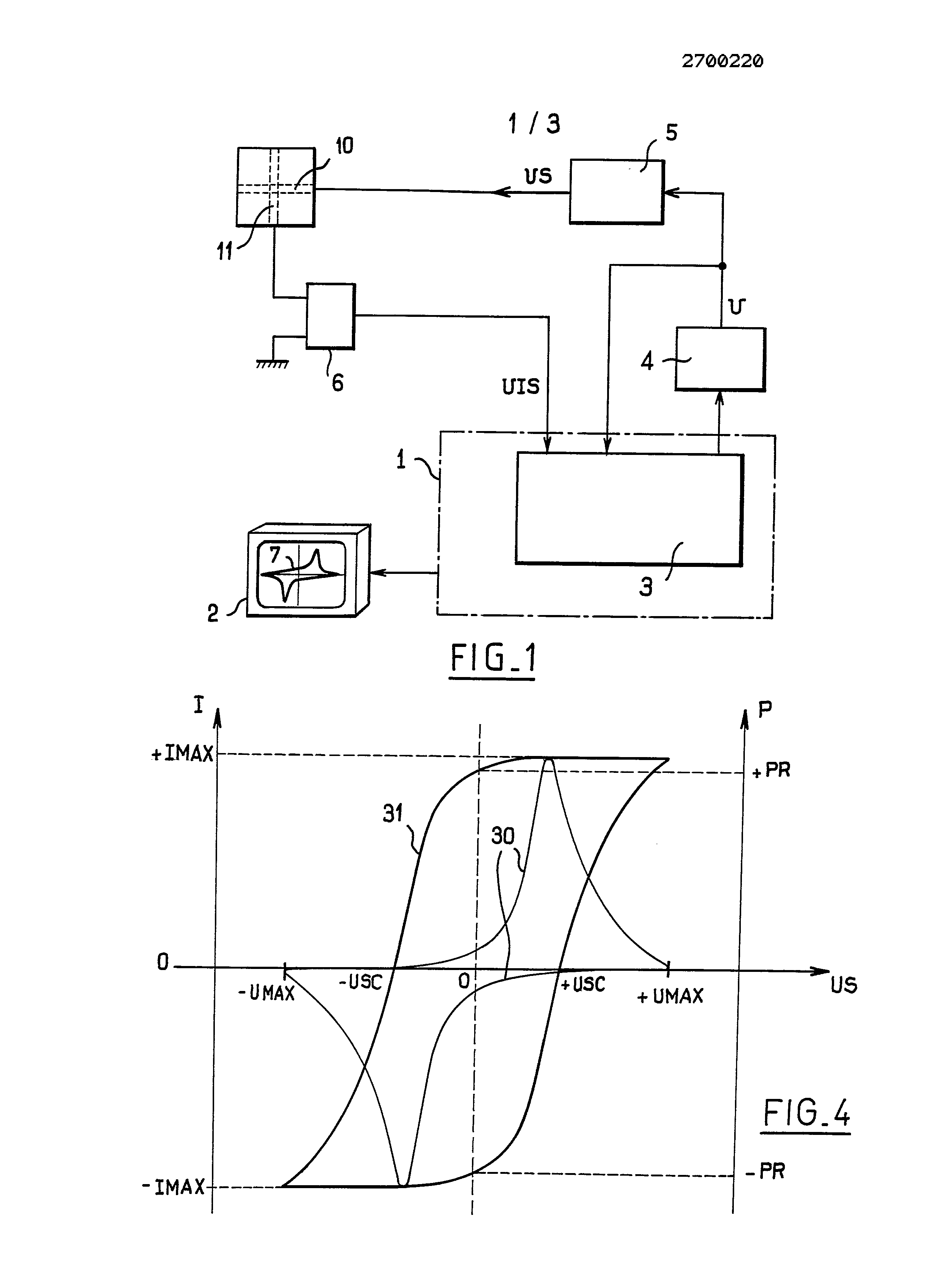
The present invention relates to a method for biasing at least one area of a sheet of ferroelectric material. The invention also provides a method for making a piezoelectric sensor or pyroelectric applying the method for polarization. In its previous request French patent FR-A -2 538,157, the Requestor has described a method and a device for polarizing ferroelectric materials. In the method, an electric field is applied low frequency alternating to the ferroelectric material, and is progressively increases the amplitude of the alternating electric field to leave a remnant polarization controlled in the material. The maximum amplitude of the electric field is relatively important because it is to be greater than the coercive field of the ferroelectric material. The method is now widely applied, in particular for making piezoelectric or pyroelectric sensors. In general, is first deposited, for example by sputtering or evaporation, the measuring electrodes of the sensor on two opposite surfaces of a sheet of ferroelectric material, and uses these measuring electrodes for applying the alternating electric field in the phase of polarization. Is compressed generally the sheet of ferroelectric material for reducing the variations of the volume that can be due to high local values of the electric field during the polarization phase, the variations in volume being one reproducibility in sensor characteristics. In practice, the pressures can be exerted on the sheet of ferroelectric material are limited, typically to a few hundred bars, and observes without damage to the ferroelectric material near the edges of the electrodes deposited, or a deterioration of the electrodes themselves if they are relatively extended. Furthermore, the respective portions of the two measuring electrodes which extend from the region biased for connection are to be relatively spaced apart parallel to the sheet of ferroelectric material. This spacing is required due to high voltages involved: there is a risk of breakdown, electrical flashover and polarization of the material if the spacing is low. As a result, increase of the size of the sensor. The above method is hardly applicable to bias an area of reduced dimensions on a sheet of ferroelectric material, typically an area having dimensions less than 1 mm2 on a sheet of a thickness of about 25 pm. For the small dimensions, edge effects become significant or predominant and complicate the interpretation of the current measurements. These effects of edge also affect the homogeneity of the remnant polarization induced. The polarization is equal to the ratio between the amount of charge and the geometric surface. Furthermore, for the small dimensions, local stresses in the ferroelectric material are large and require high pressure to limit their effect, which has problems of mechanical strength above. These drawbacks are also featured for the large surfaces, even if their consequences are small at an area measurements. A principal aim of the present invention is to overcome these difficulties of known polarization methods, by providing a method of polarization compatible with the application of a relatively high pressure, and useful preferably to bias areas of small dimensions in a sheet of ferroelectric material. The invention therefore provides a method to bias an area of a sheet of ferroelectric material, which arranges electrodes against two opposed surfaces of the sheet such that the biasing area extends in the interval between these two electrodes, is compressed the area to bias, and a variable voltage is applied between the electrodes, characterized in that each of the electrodes is bonded to a respective insulating support having an area greater than that of the area to bias on the sheet of ferroelectric material, said insulating support having, on either side of the electrode, a layer of dielectric material the thickness of which is at least twice that of the sheet of material to polarize, whose outer surface is flush with the outer surface of the electrode which further has a suitable surface smoothness. The electrodes used in the polarization phase is not related to the sheet to bias but to supports apart. The holders have each a smooth surface facing the sheet to bias, a portion of the surface belonging to the actual electrode. Therefore, if a substantial pressure is used to compress the region to polarize and thereby assert a high electric field, this pressure creates a strain which can be strong, but which is evenly distributed into the ferroelectric material and the electrode supports. The ferroelectric material, and the electrodes, will not be not damaged by this constraint. In the preferred embodiment of the invention, the electrical permittivity of said dielectric material is at least of the same magnitude as that of the ferroelectric material. This can minimize the influence undesirable edge effects in the current measurements for monitoring the polarization process. Preferably, said dielectric material and said ferroelectric material are made of the same element, the dielectric material being constituted by a non-polar phase thereof. A dielectric material, example, the PVC (polyvinyl chloride) with sr # 9 at maximum and the linear polyruéthanes with 7.5 < 6r <9. The electrodes being elongated, arranged advantageously against the opposed surfaces of the sheet so that they are substantially perpendicular to each other. The second aspect of 1' aim of the invention is a method for producing a component biased to pyroelectric or piezoelectric sensor comprising a sheet of ferroelectric material having at least a region biased, characterized in that said area is polarized of the sheet of ferroelectric material by implementing a method as defined above, and then measuring electrodes on the two opposite surfaces of the sheet, these measuring electrodes covering the region biased. The process are sensors which may advantageously have small dimensions and can be adjusted accurately and reliably sensitivity characteristics. It makes it possible to produce pressure sensors impact minimum inductive coupling. Other features and advantages of the present invention will appear in the description hereinafter of a preferred example and non-limiting, with reference to the accompanying drawings, in which: -figure 1 is a diagram of an installation for carrying out the method of polarization in the invention? figure 2-is a view schematic exploded view showing a sheet of material to polarize and two electrode supports -figure 3 is a view similar to that of Figure 2 showing the electrode supports to bias applied against the sheet; -figure 4 is a graph showing the hysteresis loops in intensity and polarization recorded at the end of the process of polarization; -figure 5 schematically shows the configuration of a shock sensor according to the prior art; and -figure 6 illustrates schematically the sensor configuration according to the invention. Figure 1 represents an installation for biasing ferroelectric materials, especially crystals, polycrystals, polymers or copolymers such as vinylidene polyfluorides (PVDF). The installation comprises analog circuits and digital circuits, but could also use in conjunction with the present invention a fully analog installation such as that described in Patent FR-A 538,157-2. The operation of the plant shown in Figure 1 is the golfing of the plant described herein. The installation of Figure 1 comprises a computer, such as a microcomputer 1 provided with a display screen 2. The microcomputer 1 is equipped with a board 3 for controlling the course of the method. The card 3 controls a low frequency generator 4 to deliver a sinusoidal voltage U at low frequency and variable amplitude. The voltage U is fed to the input of a high voltage amplifier 5 which applies the amplified voltage US to one of the bias electrodes 10. The other bias electrode 11 is carried to the zero potential of the mass. A current/voltage converter 6 is mounted preferably on the connection between the second electrode 11 to ground for measuring the current IS through the ferroelectric material in response to application of the variable voltage US. Naturally could perform the measuring the current at the first electrode. However, thereof being brought to a high potential, this measurement causes problems of technological order. The measurement is made by any method well known to those skilled in the art, said process is selected not to interfere with the current to be measured. The result of the measurement is transmitted to the card 3 in the form of a voltage signal proportional to the current UIS IS. The card 3 further receives the voltage signal U proportional to the voltage US applied. The card 3 comprises analog-to-digital converters (not shown) that convert the voltage signals U and UIS into digital signals representative of the voltage US and current IS into the ferroelectric material. These digital signals are then processed by the card 3 to display 7 curves on the screen 2 of the microcomputer, and curves representative of the signals U UIS. The arrangement of electrodes 10 and 11 is illustrated in Figures 2 and 3. Each of the electrodes 10 and 11 respectively is bonded to an electrically insulating support, 12 and 15 respectively. The supports 12 and 15 each comprise a rigid insulating plate 13 and 16, on which is deposited the elongated electrode of:10 and 11, and a layer of dielectric material: 14 and 17, whose outer surface 14a, 17a is flush with the outer surface 10a aql and electrodes 10 and 11. The thickness of the layers of dielectric material 14 and 17 is at least equal to two times the thickness of the sheet material 19 to bias. The electrodes 10 and 11 and their supports 12 and 15 can advantageously be carried out as follows: -applying the electrodes 10 and 11 on the rigid plates 13 and 16, for example by a thick film technique, to form a printed circuit; -is polished aql 10a and the outer surfaces of the electrodes on the printed circuit board; -the layers of dielectric material 14 and 17 by a spinning technique on the printed circuit board; and -is polished the outer surfaces 14a and 17a layers of dielectric material 14 and 17. The dielectric material layers 14, 17 can be, for example, PVDF phase-(non-polar phase, relative permittivity of the order of 12) or the other materials already Exemplary: PVC, linear polyurethanes, etc application of such material is carried out by forming high for the thicknesses, by a spinning technique ("spin coating", according to the Anglo-Saxon terminology), for the small thicknesses. The method includes the, a known manner, diluting the PVDF in a solution of diméthylformamyde , in an amount of 15% PVDF, to be deposited on the circuit board, a sufficient amount of the liquid mixture obtained to completely cover the printed circuit, and placing the assembly on a centrifuge that subjected to a rotational speed of 4.000 rpm for a few seconds, and then at a speed of to 6.000 5.000 rpm during a second to remove excess solution on the edge. The resulting layer has a thickness of between 2 and 4 microns. The oven the assembly to 150 °C for 24 hours. Alternatively, can be the electrode supports further by preparing a carrier having a uniform layer of dielectric material such as PVDF, and insertion of the conductive particles in a portion of the layer to form the electrode. May also implanting an electrode in the PVDF by compressing thereof in the PVDF by a conventional method of molding by passing above the melting temperature of this material (175 °C), for example 190 °C. To bias the ferroelectric material, the electrodes are arranged in 10 and 11 against the opposite surfaces 20 and 21 of the sheet of ferroelectric material 19, such that the electrodes 10 and 11 are substantially perpendicular to each other, as seen in Figures 2 and 3. Other configurations are feasible: the electrodes can be, for example, circular or annular and face each other. The area to bias 22 extends in the gap between the two electrodes 10 and 11. The insulating supports 12 and 15 each have a larger area than the biasing area 22 on the sheet of ferroelectric material 19, so that by exerting pressure on the supports 12 and 15, can be compressed homogeneously the biasing area 22 and a portion of the sheet 19 surrounds this region. The applied pressures and can advantageously be important, typically in a pressure range of the order of 50 to 200 MPa according to the materials considered. Once the sheet 19 has been compressed, the card 3 controls the generator 4 to deliver a voltage U very low frequency (in the order of hundredths of hertz) and amplitude slowly growing up to a value corresponding to, after amplification by the amplifier 5, to the application between the electrodes 10 and 11 of an electric field greater than the coercive field of the ferroelectric material to polarize. Meanwhile, UIS U and the signals representing the voltage and the current US IS in the area to bias 22 are processed to extract the resistive components IR and capacitive current IC IS. IR The resistive component is calculated according to the formula IR = US/R where R denotes the internal resistance known to the ferroelectric material. The IC capacitive component is calculated according to the formula IC (dUS/dt) = ε where ε denotes the known permittivity of the ferroelectric material and the ratio (dUS/dt) denotes the time derivative of the boosted voltage US. After subtraction components IR and IC, there is left a polarization component = (dP/dt) IP = IS-IR-IC. The component is equal to the time derivative of the polarization P in the ferroelectric material. During the process variations in the polarization component IP function of the applied voltage US are displayed on the screen 2 of the microcomputer 1, in the form of a hysteresis loop 30 (Figure 4) having two peaks symmetrical about the origin. The value of the P polarization is calculated by integration of the current IP, and its variations in US are also displayed on the screen 2 in the form of a hysteresis loop 31. The display cycles 30, 31 ensures their stabilization of the end of the process. When the voltage US is suppressed, remains in the region 22 of the sheet 19 a remanent polarization PR indicated in Figure 4. It has been found, after experience, that for a same material, the maximum values of IP are identical for the polarized elements at the same voltage level: this means that the invention ensures the reproducibility of the desired effect. The above method can be used for making piezoelectric or pyroelectric sensors. After having separated the electrode supports 12, 15 of the sheet 19, are deposited measurement electrodes on the two opposing surfaces 20, 21 of the sheet so that the measuring electrodes previously grown cover the region biased 22. The measuring electrodes can be arranged in a compact configuration, for example one above the other, to obtain a small sensor, while, with the previous processes in which the measuring electrodes are also used in the process of polarization, the electrodes were to be relatively spaced. Figures 5 and 6 schematically illustrate two examples of sensor configuration, one (Figure 5) relative to a sensor designed according to the prior art, the other (Figure 6) in accordance with the teachings of the invention. The two sensors comprise a support 19 based on one of the mentioned ferroelectric materials. The sensor of Figure 5, of the known art, has a set of electrodes disposed on either side of the carrier 19. The electrodes include an overlap area 102 (hatched line in Figure 5) or active area and elongate areas 100 and 101 for contact outlets and • The electrodes were used to the polarization of the material of the support 19 and thus the spacing e between their projections on a plane parallel to the support 19 either be sufficient to prevent the parasitic effects that have been described. Any on the contrary, in the case of a sensor made in accordance with the present invention, as shown in Figure 6, there is also an overlap area 202 or active area (hatched line in Figure 6}, as for the sensor of Figure 5, however the distance e 'between the elongated lands 201 and 202, contact outlets C' -' ^ and C2 can be reduced to its simplest expression: the spacing e ' may be zero. Indeed the measuring electrodes are performed after the phase of polarization of the material in the overlap region 202, according to one of the important features of the method of the invention. As a non-limiting example, the sensor device may be used as impact sensor. The configuration of the sensor, as depicted in Figure 6, to achieve a minimum inductive coupling. Measurements showed that the inductance of a sensor having a configuration as depicted in Figure 6, was fifty to eighty-fold less than that of a sensor equivalent, but conducted in accordance with the known art: Figure 5. As a result recess that the impact sensor thus produced is efficient that a conventional sensor. The area to bias 22 can be large and especially can advantageously have reduced dimensions, for example less than 1 mm. At this time, it is preferable that the electrical permittivity of the dielectric material of the layers 14 and 17 is at least approximately the same as that of the ferroelectric material of the sheet 19, for reducing the influence of edge effects on the current measurements. In particular it is convenient the materials of the layers 14 and 17 and 19 of the sheet from a single element such as PVDF. The PVDF is then in phase non-polar in the layers 14 and 17 and polar β phase (ferroelectric) in the sheet 19. The method of the invention has been tested by the applicant, in particular in the example of a sheet of PVDF phase β thickness pm 26, with a region biased dimensions of 0.53 mm x 0.57 mm (0,003 cm area2 ). The coercive force in the material corresponding to a voltage of about 2.2 USC kV, first applied between the electrodes 10 and 11 a sinusoidal voltage US of 0.04 Hz frequency whose amplitude grew of 0 to 3 kV for 55 minutes, then a sinusoidal voltage US of 0.02 Hz frequency whose amplitude of waxed kV during 95 3 to 5 minutes. At the end of the step of biasing, with the maximum amplitude = 5 UMAX kV of the voltage US, is observed hysteresis loops 30 and 31 such as those shown in Figure 4, with a maximum bias current of about 0.0138 μΑ IMAX. The remnant polarization PR has been selected equal to about 6.7 pC/cm2 , and the piezoelectric coefficient d33 pC is about 15/D. Furthermore, it has been found, surprisingly, that the use of this device has been found capable of biasing of the large surfaces of ferroelectric polymers unexpectedly by reducing the breakdown due to the edge effects. Although the invention has been described with reference to particular embodiments, it will be understood that these examples are not limiting and that various modifications may be made without departing from the scope of the invention. The especially copolymers instead of polymers as materials that form the support to bias. Include by way of non-limiting example the vf2 / vf3 . A method of polarizing selected areas of a foil of ferroelectric material, wherein electrodes are deposited in such a way on the opposite surfaces of the foil that the zone to be polarized extends between these two electrodes. The zone to be polarized is compressed and a variable voltage is applied across the electrodes. Each electrode is connected to an insulating support whose surface exceeds that of the zone to be polarized on the foil of ferroelectric material. Besides the electrode, the insulating support has a layer of dielectric material whose external surface is level with the external surface of the electrode. 1. A method for biasing at least one area (22) of a sheet of ferroelectric material (19), which arranges electrodes (10, 11) against two opposing surfaces (20, 21) of the sheet (19) so that the area to bias (22) extends into the gap between said two electrodes (10, 11), the region is compressed to bias (22), and a variable voltage is applied between the electrodes (10, 11), characterized in that each of the electrodes (10, 11) is bound to a support respective insulation (12, 15) having an area greater than that of the area to bias (22) on the sheet of ferroelectric material (19), said insulating support (12, 15) having, on either side of the electrode (10, 11), a layer of dielectric material (14, 17) whose thickness is at least twice that of the sheet material (19) to bias, and whose outer surface (14a, 17a) is flush with the outer surface (10a, aql) of the electrode (10, 11). 2. A method according to claim 1, characterized in that the electrical permittivity of said dielectric material is at least of the same magnitude as that of the ferroelectric material. 3. A method according to claim 2, characterized in that said dielectric material and said ferroelectric material are made of the same element, the dielectric material being constituted by a non-polar phase thereof. 4. The method of any one of claims 1 to 3, characterized in that each insulating support (12, 15) comprises a rigid plate (13, 16) forming a printed circuit with an electrode (10, 11) deposited on the plate (13, 16). 5. The method of any one of claims 1 to 3, characterized in that forming an electrode on a support having a uniform layer of dielectric material by implanting conductive particles in a portion of said layer of dielectric material. 6. The method of any one of claims 1 to 5, characterized in that the insulating supports (12, 15} carrying the electrodes (10, 11) ferroêlectrique compress the sheet of material in a pressure range between 50 MPa and 200 MPa. 7. The method of any one of claims 1 to 6, characterized in that the electrodes (10, 11) are of elongate shape, and to dispose the electrodes (10, 11) against the opposite surfaces (20, 21) of the sheet (19) so that they are substantially perpendicular 1 'to 1' other. 8. The method of any one of claims 1 to 7, characterized in that the ferroelectric material (19) is a polymer. 9. The method of any one of claims 1 to 7, characterized in that the ferroelectric material (19) is a copolymer. 10. The method for making a sensor element biased to piezoelectric or pyroelectric ferroêlectrique comprising a sheet of material (19) having at least a region biased (22), characterized in that said area is polarized (22) of the sheet of material ferroêlectrique (19) by carrying out a method according to one of claims 1 to 9, and then measuring electrodes on the two opposite surfaces of the sheet (19), these measuring electrodes covering the region biased (22).