USING A REFERENCE BIT LINE IN A MEMORY
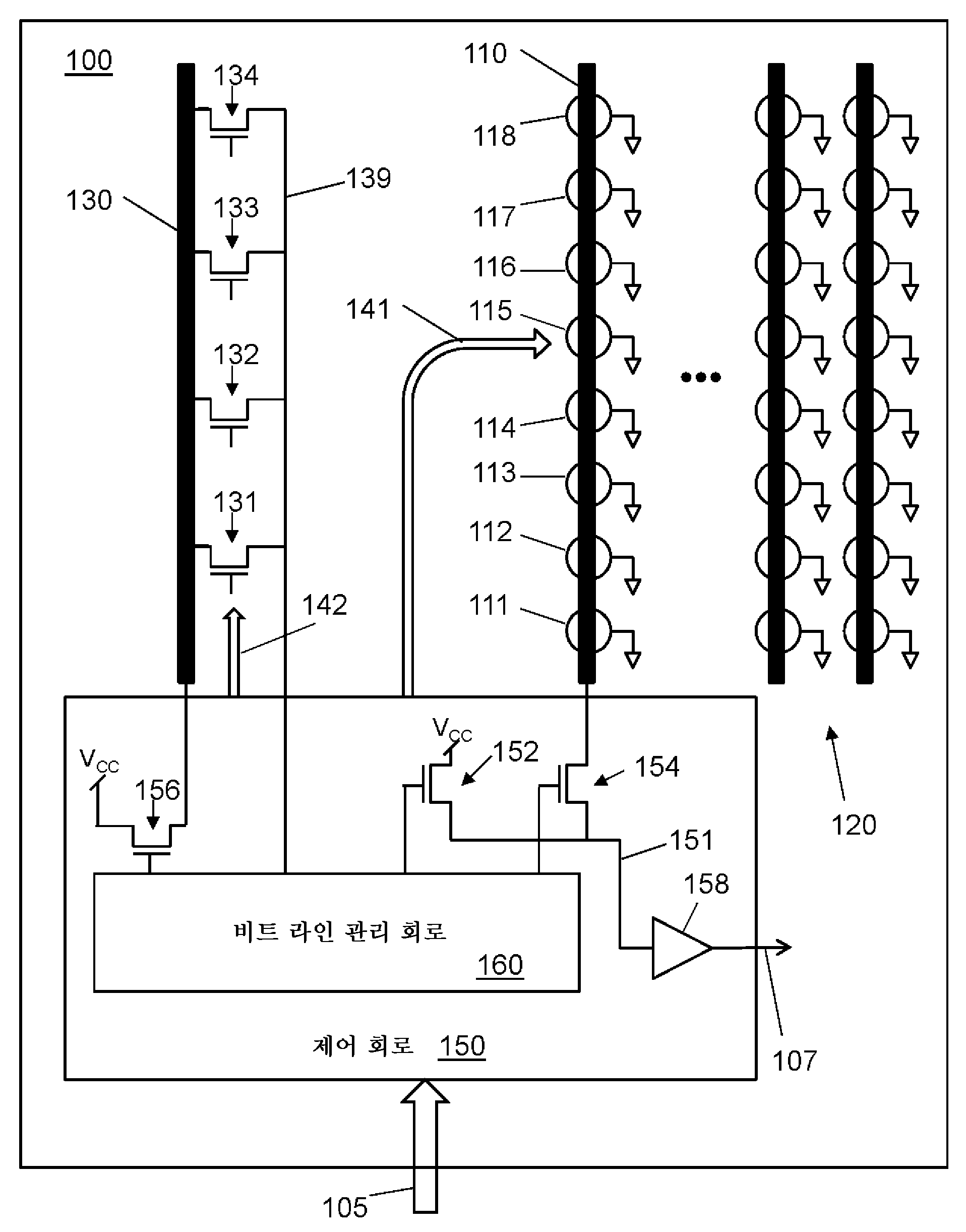
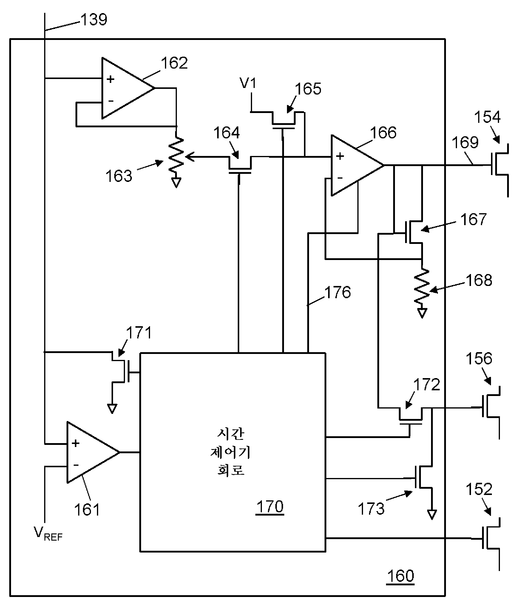
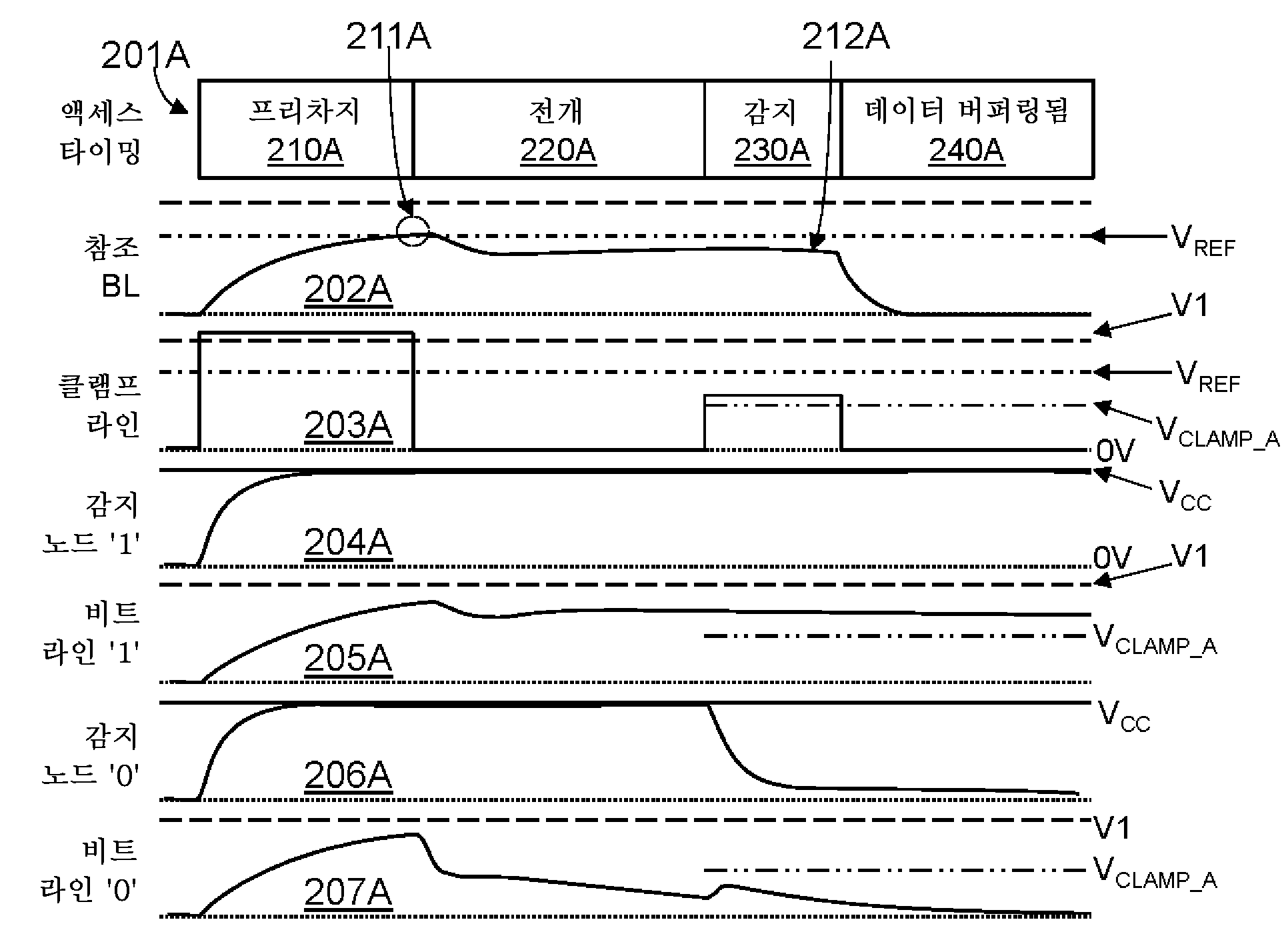
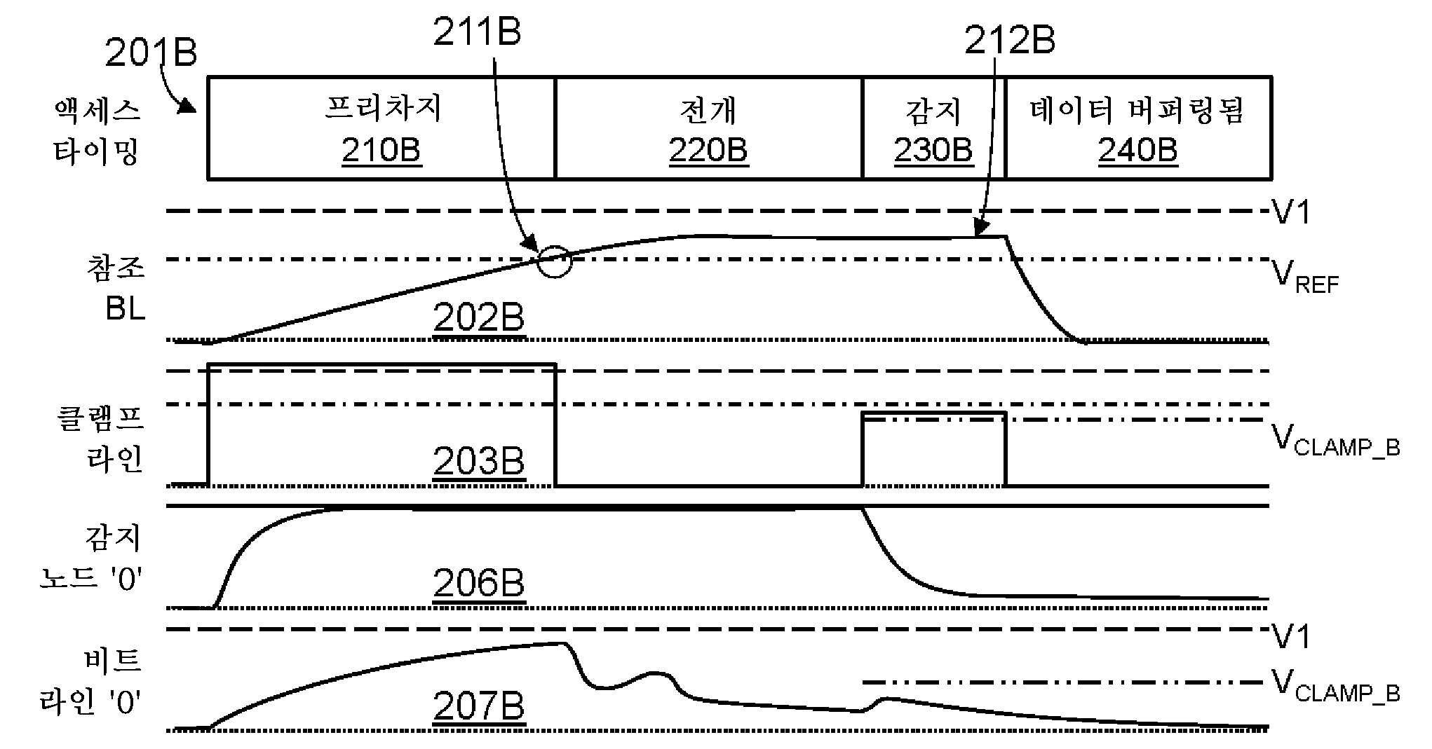
Machines as semiconductor memory is provided to the present invention, more specifically, memory for controlling access relates to. Many types of semiconductor memory is described is publicly known to the field of. Types memory of the memory cell charge storage region storing a charge in. a flash memory. Threshold voltage of MOSFET (metal-oxide-semiconductor field-effect transistor) based flash cell (flash cell) cells with stored in charge storage region by changing the quantity of the charges can be changed and, threshold voltage represents the value stored in the flash can be used. 2 flash cell threshold voltage of different States is made from a first voltage source between the provided thereacross in the flash cell by, flash is flash cell that measures current passing through through can be determined by. Flash cell (off-current) off current much higher. present on the first has a (on-current). Flash memory NAND and currently commonly used one architecture is architecture. NAND architecture wherein an, 2 two or more memory cells to engage each other into two wavelengths through the optical (string) string is, individual silicon wafer and is coupled to the word line. NAND string in one end of NAND string can be combined. bit line. Is PCM (phase change memory) memory of the other types. PCM distributed in the nonconductive amorphous state and conductive crystalline state in which the wireless telecommunication device use of phase change of the phase change material. PCM cell, the value stored to indicate one state or other state and can be. PCM cell voltage across the by providing, PCM PCM is that measures current passing through through the cell can be determined by. PCM significantly longer than off current cell has a current low temperature. PCM flash memory and including a number of types of memory memory cells' Y 'direction' X ' and can intersect array and in both control lines can construct, in an array having. These control line may have many different names generating often the, but can be, referred. Control line are quite long and, its length coupled to and control lines assigned to number keys of the selected memory cells, high resistance and capacitance material may have a. Included in specification of the portions thereof in the embodiment a variety of accompanying drawing indicative of wet liquid to flow down. In overview, elucidation with, describes the principle various drawing serves make. Also the memory of the first deoxygenator 1a embodiment. Also filter in memory 1b embodiment of the first deoxygenator. Also in the embodiment of the memory 2b and 2a in timing is also advanced or delayed, of on-line. Embodiment of Figure 3 the first deoxygenator flow right chart method access is made to the EDID memory. Figure 4 shows a one embodiment of an electronic system also the first deoxygenator block. Inhibit the growth of hematopoietic stem cell in the description hereinafter, associated disclosure content understanding complete number of spheres to provide, for example, details disclosed is as. However, the present disclosure embodiment without the contents can be her it is apparent that those skilled in the art will. That would otherwise, the present general outline ambiguities superfluous sides of a in order to avoid, a publicly known method, procedure relatively without-specific and components is outlines. Various content of disclosure is used in the embodiment describes syntax terms and plurality of descriptors for. is processed by using. The syntax terms and described these, the present specification to another definition is a that are not given, generally to one skilled art agreed is use in transmitting the meanings. From now on, hereinafter discussed in accompanying drawing is illustrated, for example. to dually function as a pipeline and detailed. Also the memory 1a (100) the first deoxygenator embodiment of is. Memory (100) the bit line (110) and additional bit lines (120) variety of can be conductor-containing. "Bit line" is term are generally art although the understood by one skilled in the art, other names are hi some techniques can be used. The bit line, is the terms had the present specification as used in claim and, the line is bound to the memory of one of the cells for sensing state of memory cell that can be used, one or more 2 any be connected to plural memory cells speak of conductors can be. Bit lines (110,120) .may be part of a memory array. Bit lines (110,120) the, each, bit line (110) is bound to the memory cells (111 to 118) such as one or more memory cells coupled to 2 may be proposed. In any in the embodiment, memory cells (111 to 118) the same bit line (110) are coupled separately to an but may be, NAND string architecture wherein an other in the embodiment are arranged as a plurality of memory cells may have predetermined locations wherein data, in one end of the string and string is coupled to bit line. Memory cells (111 to 118) the, any memory cells (111 to 118) is other memory cells than sense node (151) further so as to be proximate to, bit line (110) are distributed over the may be proposed. In shown, memory cell (111) is sense node (151) most close proximity with and, memory cell (118) is sense node (151) remotest from. Memory cells (111 to 118) the in addition is coupled to ground (conductive state) conductive condition can be (non-conductive state) non-conductive condition and may have a, when conductive condition is a memory cell according to the, bit line (110) is electrical charges which are on the discharge to the ground through memory cell can be (drain). Memory cells are NAND string when arranged in, the ground one end of NAND string can be is coupled to, the string are that every memory cell of. electrical continuity between string when conduction (conductive). Bit line (110) is bound to the memory cells (111 to 118) in memory to select that cell word line (141) such as additional memory control line may be provided. Reference bits line (reference bit line) (130) may include. Reference bits line (130) other bit lines (110,120) substantially similar to that of a can take the electrical characteristics. In any in the embodiment, reference bits line (130) of a different length of is substantially equal to bit lines can be. In any in the embodiment, reference bits line (130) length of, a resistance and capacitance, each, bit line (110) of at least one of bit line such as length of bit line, resistance and capacitance about 10% may be proposed in. Bit line (110) of resistance and capacitance various embodiment examples between different from each other although it is possible, in any in the embodiment, bit line (110) total resistance of about 1 mega package (overall resistance) (MΩ) to about 5 M Ω and the shaft transfers the, bit line (110) (lumped capacitance) capacitance (pF) farad picocell concentration of about 1 to about 2 pF can be. Bit line (110) also length of embodiment examples between different from each other although it is possible, in at least some in the embodiment, bit line (110) of length of about 1 millimeter (mm) to about 3 mm can be. Bit line (110) and reference bit line (130) as the voltage bit line (110) as measured along line reference bits whether (130) as measured along depending electric waveform is provided to enable easy can vary and may serve as an transmission line. In any in the embodiment, reference bits line (130) the memory array but may be included in, other in the embodiment are memory array outside the region reference bits line (130) may include a. Reference bits line (130) is coupled to the memory cells can be non-or otherwise, a structure to simulate capacitance memory cell may comprise an. In any in the embodiment, reference bits line (130) the bit line (110) is bound to the memory cells (111 to 118) not being accessed simultaneously coupled to memory cells available may be proposed. Reference bits line (130) a reference bit line (130) are distributed over the different voltage to provide detection location 2 may include one or more tab. Any number of tab in various in the embodiment may be provided but, in the embodiment are bit line (110) is coupled to tab is an amount that is less than the number of the memory cells reference bits line (130) can be provided on. In any in the embodiment, bit line memory cells are several thousand and wound in a water (110) may be coupled to even, such as 256 of tabs or the same small number of tab hereinafter may be provided. In at least one in the embodiment, reference bits line (130), and to introduce only on may be provided but two tab 4,8 are two other in the embodiment, one or two 32 provides tab 16. (Pass transistors) pass transistors tab (131 to 134) by voltage monitoring line (139) can be is coupled to, voltage monitoring line (139) the control circuit (150) is coupled to. Control circuit (150) password transistors (131 to 134) the capacitive load is selectively one of the display part to display tab the, pass transistors (131 to 134) of control gate is tap selector line (142) can be driven by. Memory (100) the in addition control circuit (150) may comprise an. Control circuit (150) has pass transistors (154) [any in the embodiment in, the composition can be taken 2-negative clamping transistor (clamping transistor)] the bitstream syntax is described by line (110) which may be coupled to sense node (151) may comprise an. In any in the embodiment, selects one of bit lines of several password transistor (154) can be coupled to multiplexers are to allow a can be used. Further expanded in their hereinafter will be discussed in greater detail below as bit line (110) are addressed basis of the voltage level of a state of the memory cell to detect, buffer (158) (sense gate) is sense node gate is detected (151) is coupled to may be proposed. Buffer (158) output of (107) the, according to embodiment, addressed state of the memory cell in the reversal of state or may be provide (inversion) by using the mask pattern.. Control circuit (150) the memory (100) external access is made to the EDID memory which may be couples to the source address and/or command line (105) is capable of receiving a.. Control circuit (150) the line (105) which indicates that the data is not read command (command), write command, erase command and/or specific program instructions can be to respond to a command. In any in the embodiment, a read control circuit in response to a command and buffer (158) output of (107) such as those that are indicated by the state of the memory cell is addressed and/or may be provide write, to respond to a command program or erase state of the memory cell are addressed.. Pass transistor (152) [any in the embodiment in, charging transistor (charging transistor) the composition can be taken 2-negative] has a sense node (charge source) the charge source (supply voltage VCC such as) permit bonding to. Pass transistor (156) has reference bits line (130) of the charge source (supply voltage VCC such as) includes so as to obtain bonding of may be proposed. Pass transistors (152, 154, 156) control gate a bit line management circuit (bit line management circuitry) (160) (one of its embodiment substracte also 1b is shown thus to negative) can be are driven from. Bit line management circuit (160) at least in response to the memory command (memory command) two different 3 further expanded in their hereinafter-period and therefore is free discussed in greater detail below a precharge period, deployment period (development period) for-sense periods and can be disclosure. In any in the embodiment, memory (100) are used the plurality of bits of the a plurality of bit lines may be simultaneously access a by. In such in the embodiment, respective individual sense node respect to bit lines (151), buffer (158) and pass transistors (152,154) can be is provided. Also the memory 1b (100) bit-line to bit-management circuit (160) for including one control circuit is the first deoxygenator embodiment. Memory in response to a command, bit line management circuit (160) receives pre a precharge period can start an.. During a precharge period, a selected bit line (110) of memory cells (111 to 118) selected non-conductive is decompressed and. can be at. In any in the embodiment, memory cells (111 to 118) the memory cells (111 to 118) which are each coupled to word lines (141) (deassert) [...] of speaking by the second device, in the embodiment other memory cells (111 to 118) to place its non-conductive condition for alternate matter can provide a mechanism. At the start of a precharge period, reference bits line (130) across the length of the bolt having a voltage level (V) about 0 the can be at.. Tap selector lines (142) by asserting one of tab (assert) can be selected. Addressing memory cells address based at least in part, can be selected tab. Addressed from the plurality of memory cells sense node (151) based at least in part with regard to its distance to, can be mapping tap address. Therefore, memory cell (111) is sense node (151) to nearby when the addressed memory location, pass transistor (131) control gate high for by driving a first tab can be selected. Memory cell (118) is sense node (151) distal from when an addressing memory where the, pass transistor (134) by driving the control gate high for last tab can be selected. Tab the selection of a voltage monitoring line (139) reference bit line (130) to coupled to certain point. During a precharge period, time control circuit (170) the, pass transistor (152) by enabling a supply voltage VCC a sense node (151) by the engagement of a, sense node (151) in logic high. level. Supply voltage VCC the voltage level of the high voltage embodiment but, can be varied according to, pass transistor (154) and pass transistor (156) to the control gate of is supplied with various voltages and is larger than, in any in the embodiment, can be about 3 V. During a precharge period, time control circuit (170) the in addition, pass transistor (164) while disables, pass transistor (165) by enabling a voltage V1 an operational amplifier (166) non-inverse input of can be passing. Pass transistor (164) and pass transistor (165) one a P-without enable a P-other enables the 2 to 1 multiplexer by a (two to one mux) can be used. Time control circuit (170) has enable line (enable line) (176) operated upon using a amplifier (166) may decrease from a reference. Operational amplifier (166) has enable line (176) this high when the but can function as a operational amplifier, an enable line (176) when approximately its output is low or off to ground. Transistor (167) with its source and control gate is operational amplifier (166) is coupled to an output of, operational amplifier drain thereof (166) of a shift and transistor (167) resistor flow means for providing a flow of the current through the (168) is coupled to. In any in the embodiment, resistor during idle period (idle period) (168) by removing the current through the assembling test, an enable line (176) is controlled by pass transistor, and a method for manufacturing the same are adjusted.. Shown configuration is a "voltage V1 + transistor (167) (time offset before and after each other transistors corresponding to the may be indicative of a negative) the threshold voltage of the resulting Vt" substantially the same charging voltage clamp the line (clamp line) (169) can be provided via the. Clamp line (169) the bit line (110) for sense node (151) that bundle pass transistor (154) is coupled to the control gate of may be proposed. This configuration allows adjacent, during a precharge period, VCC pass transistor charge from (152) detecting node (151) to and sense node (151) from pass transistor (154) through the bit line (110) .can be supplied. Time controller (170) has pass transistors (172) by enabling a clamp line (169) for pass transistor (156) by the engagement of a reference bits line (130), for supplying electric charge to the can be, the feed to voltage VCC charge from a data section results in a reference bit line (130) the fluid can flow into to allow a. Reference bits line (130) of of the selected tap to the voltage monitoring line (139) can be monitoring through. Comparator (161) has a voltage monitoring line (139) with a reference voltage VREF and compares, voltage monitoring line (139) is reference voltage VREF can exhibit access is provided to the electronic content. In any in the embodiment, addressed address or memory cell accessed from memory cells sense node (151) according to the distance the reference voltage VREF. can be changed. In at least one in the embodiment, sense node (151) further away from a device linked reference voltage VREF may be layer includes a plurality of contact. Bit line reference at the selected tap (130) voltage of reference voltage VREF to be connected to either a storage, time control circuit. capable of terminating a precharge period. Time control circuit (170) at the end of a precharge period the preset can take several measures. Time controller circuit a clamp line (169) activated by an enable driven by the bit line (110), for supplying electric charge to the stopping in which the antenna is enabled for line (176) for [...] by operational amplifier (166) disables the. As such, bit line charge (110) supplied to time (a precharge period the composition can be taken 2-negative) referred to in the comments bit line (130) voltage of reference voltage VREF, the time to reach the. may be based on. Time control circuit (170) the in addition, pass transistor (156) turning off the reference bits line (130), for supplying electric charge to the stopping to, pull-down transistors (pulldown transistor) (173) and turns the password transistor (172). turning off. Time control circuit (170) the in addition sense node (151) charging a pass transistor to thereby terminating (152) but the turning off, other in the embodiment are pass transistor (152) turning off the. delay until later visual. Reference bits line (130) the same bit line (110) is substantially equal to electrical characteristics is connected to a gate, during a precharge period bit line (110) voltage of reference bits line (130) voltage may substantially similar to at. Thus clamp line (169) is reference voltage VREF significantly more than even for higher voltages, bit line (110) voltage of reference voltage VREF does not exceeds a lot of the capacity ratio thereof can reach. During a precharge period clamp line (169) through a higher charging voltage when the, pass transistors (154,156) control gate and a high-difference and resistor-capacitance (R-C) removed from a charging, bit line (110) and reference bit line (130) is. can be filled faster. Therefore, charging voltage reference voltage VREF may be higher than. In any in the embodiment, charging voltage reference voltage VREF at least 200 millivolt (mV) may be higher. In any in the embodiment, reference voltage range of about 300 mV to about 600 mV can be, about charging voltage range of 1.0 V to about 500 mV may be proposed. After the precharge period, bit line (110) is bound to the addressed memory cells can be selected. By selecting a memory cell, memory cell, or the erased state '0' state such as when the number 1, can be electrical continuity between, '1' state set state when a compressed state another payload such as may non-unified. In any in the embodiment, a single-memory cell indicate ' don't plurality of of bits of information may be stored to allow a single memory cell is one or more 3, may have an activated but, is by the current through the cell detectable a, memory cells is selected can be deemed. In any in the embodiment, be connected to plural memory cells by asserting a word line can be selected memory cells. In using NAND architecture in the embodiment, non-addressed cells are NAND string, by using a water-amount sensor thereof, can be the coulping, the cell is addressing can be selected. Is selected memory cell is addressed, time control circuit (170) the bit line (110) and the charge stored in the cell is stabilized addressing when the cell is electrical continuity between the interior charge to allow a deployment period by using the mask pattern.. Bit line (110) in transmission line (transmission line) removed from a bit line (110) is pre after the end of a precharge period and/or electrolytically for stabilizing the bit-line (110) that a period of time for a distribution throughout the some to account for the can be a vortex size is reduced while the. Capacitance and resistance over the length distributed reference bits line (130) due to length of, longer charge even if second channel sound signal, and outputs, selected tap a reference in bit line (130) after the end of a precharge period voltage of may be varied. Charge reference bits line (130) to one end of supply, and can be made, than opposite from end reference bits line (130) of charge at the end can be more, the capacity ratio thereof can reach voltage thus. For unrolling along period, charge reference bits line (130) can be distributed over the. Reference voltage pass transistor order to compare and a V (131) when selected tab by enable the vicinity of, deployment in a second step, after the reference voltage the voltage at tap thereof VREF may be lower than. Pass transistor (134) through which the tab distal by enable selected when, deployment in a second step, after the reference voltage the voltage at tap thereof VREF may be higher than. In a second step, after the deployment, time control circuit (170) a sense period can be disclosure. Sense periods at the start of, sense node (151) to the supply voltage VCC the switching device corresponding to from, pass transistor (152) is, if this is not the case turned off prior to, can be turned off. Reference bits line (130) is of stability of voltage level and to float by connection to a to allow a pass transistor (156) is in an off state, a can be while, reference bits line (130) based at least in part on voltage clamp setup can be. Voltage monitoring line (139) is configured as a unit gain amplifier (unity gain amplifier) the computational amplifier (162) to the positive input of the can be combined.. In any in the embodiment, clearance voltage (margin voltage) may be selected to allow a voltage divider (voltage divider) (163) are adjusted.. The voltage divider (163) a fixed voltage divider (fixed voltage divider), packaging and during the testing stage fixed or during operation which can be selected multiple, selectable (resistive ladder) resistor ladder having tabs, diode or transistor and a resistor or supply earthed by means of a fixed voltage to the voltage drop (fixed voltage drop), or clearance voltage reference bits line (139) is subtracted voltage from any permit the in-can be other circuitry. In at least one in the embodiment, clearance voltage variable in a range of about 50 mV to about 200 mV can be effected. "Reference bits line (130) at cross clearance voltage" substantially equivalent to that of the operational amplifier the circulator to the clamp voltage level (166) be provided to to the positive input of the pass transistor (164) and turns the password transistor (165) voltage divider by turning off (163) for passing output of the 2 to 1 multiplexers are control can be. Sense periods during "the circulator to the clamp voltage level threshold voltage + Vt" the same a control voltage this clamp line (169) through the pass transistor (154) to the control gate of be provided to an enable line (176) for asserting by operational amplifier (166) may be enabled during sense periods is.. Clamp line (169) is "the circulator to the clamp voltage level threshold voltage + Vt" and a when same voltage level as that of a, pass transistor (154) the, at least one of the voltage at the other terminal if it is less than the circulator to the clamp voltage level, can conduction. Therefore, selected memory cells is non-conductive condition when, bit line (110) a reference bit line (130) voltage substantially equivalent to that of the voltage and, a supply voltage sense node VCC is. The circulator to the clamp voltage level reference bits line (130) and low-voltage clearance than of, reference bits line (130) charging the voltage of the supply voltage was used the VCC since the smaller than that of, pass transistor (154) conduction during sense periods is may not. Pass transistor (154) if not conductive, sense node (151) so that the charges at can be non-is discharged, sense node (151) logic high and a change in the voltage of sense periods during. may be held in level. Selected memory cells when conductive condition, bit line (110) to deploy through period the selected memory cell and may otherwise have to be discharged via, thus bit line (110) a reference voltage VREF can be to voltages lower than the 0 V can be near a. Bit line (110) this clamp when voltages lower than the, sense node (151) sense periods is charge from bitlines during (110) and the, bit line (110) mass of the sense node (151) and significantly longer than capacitance of, selected memory cells the same bit line (110) from charge is continued to ground since the, there can preferably be, sense node (151) voltage of bit line (110) voltage (0 V can be near a) can and the nearer the, sense periods during can be detected as level logic low. Therefore, bit line is memory addressed (110) the basis of the voltage level of is able to be determined. In any in the embodiment, sense lines on erased level logic low '0' may correspond to the state, logic high and a change in the level set '1' corresponding to at least two color pixels although it is possible, other corresponding relation between the are in the embodiment can be input data according to the first and, another in the embodiment are a plurality of bits to represent large number of voltage levels, use can be made of,. Sense periods after the, transistor (171) applied through the reference bits line about 0 can be discharge portion with a bolt. In any in the embodiment, reference bits line (130) over the entire length of the backward in the to accelerate about 0 V is also provided to help the, transistor (171) is turned in during plurality of pass transistors (131 to 134) can be turn-on time of a parasitic. Eliminate a point, control circuit (150) substracte the present specification only one of embodiment but are described in, the same one skilled art for behavior, and for many other circuit in the embodiment are behavior and design the ability to use a description of.. A circuit used according to the description, other circuit topology shown in 1a and 1b also more efficient or less efficient first can be effected. Also 2a and 2b has door 1a and 1b is shown in the memory such as (100) in the embodiment of in the timing of the on-line features. Also to make the memory cell 2a (111) such as sense node (151) in close proximity with the and concerns a access a memory cell, also 2b to make the memory cell (118) such as sense node (151) distal from. concerns a access a memory cell. 2a also now refers to surface, access timing indicator (201A) the memory (100) which may be access is formed in two different 4. mm for matching period. A precharge period (210A) the bit line (110) and reference bit line (130) characterized by time filled with may it erases, quality. Deployment period (220A) bit line is selected and the memory cells (110) is selected voltage which depends on the state of a memory cell can be stabilized may it erases, quality characterized as time. Sense periods (230A) the sense node (151) is selected and which can exhibit state of the memory cell can it erases, quality characterized as time, data buffering period (240A) is latched or not the data read from the memory, or returned as read data, validated or, other which may utilize the manner in period may it erases, quality characterized as. Reference bits line (130) of voltage waveform (202A) the sense node (151) a memory cell in close proximity with the (111) exhibits and access. Memory cell (111) is sense node (151) since the in close proximity with the, pass transistor (131) a enables the other tabs the other on the pass transistors (132 to 134) by disabling the reference bits line (130) from first tab can be selected. 2 two different access is also is shown in a 2a. Waveforms (205A and 204A) as illustrated at non-conductive access to the '1' state in a selected memory cell (111) relates to, waveforms (207A and 206A) as illustrated at a second access a continuity '0' in a selected memory cell state (111) which, waveforms (203A and 202A) these access to both 2000. Pass transistor (152) is a precharge period (210A) during can be turn, sensed thereby node (151) the, sense node '1' waveform (204A) and sense node '0' waveform (206A), as shown in, supply voltage VCC. raised to level layer to the extent that the contact. Clamp line waveform (203A) the bit line (110) is coupled to pass transistor, and (154) blades, presenting a voltage at the control gate for the unselected non. Pass transistor (156) in addition the control gate of a precharge period (210A) similar during can be voltage. Clamp waveform (203A) the selection signal has a first period (210A) voltage during exhibits a high voltage of slightly more than V1. Waveform (202A) and waveforms (207A and 205A) as shown with codes, a precharge period (210A) charge during password transistor (154) and pass transistor (156) through the, each, bit line (110) and reference bit line (130) can be supplied to. Reference bits line (130) the point in time (211A) in reference voltage VREF to be connected to either a storage, waveform (203A), as shown to, pass transistor as well as line clamp (152) and pass transistor (156) by driving the control gate into the earth a precharge period (210A) can be is terminated. Subsequent period, and a deployed (220A) during, waveform (202A), as shown in, reference bits line (130) can be voltage lines are formed of. Selected line reference bits a tab (130) since the close proximity of the beginning of a, reference bits line (130) the voltage reference voltage stabilized VREF of slightly more than can low, the reason is that a charge reference bits line (130). because distribution throughout the. Deployment period (220A) memory cell addressed during can be selected is (are). Sense node (151) representing a waveform (204A) and non-conductive '1' in a selected memory cell state (111) bit-line to bit-(110) waveform indicative of (205A) examples of having two 2. it is shown. Waveform (206A) the sense node (151) indicates the, waveform (207A) the conduction '0' in a selected memory cell state (111) bit-line to bit-(110), presenting a. Waveform (204A) and waveform (206A) both the, pass transistor (154) since the is in an off state, a, deployment period (220A) during improve its electrolytic holding the rights sense node (151) exhibits and. Waveform (205A) the, in a selected memory cell (111) is non-corrupted when, bit line (110) referred to in the comments bit line (130) similar voltage stabilized. indicate that it can. Waveform (207A) the, in a selected memory cell (111) when the are electrically connected, bit line (110) to deploy through period (220A) can be pulls down during, deployment period (220A) as the voltage in the vicinity of ground at the end of low. indicate that it can. Thus sense periods (230) during, the circulator to the clamp voltage level VCLAMP_A the, prior as described above, reference bits line (130) voltage (212A) based at least in part on. can be set. The circulator to the clamp voltage level VCLAMP_A has reference bits line (130) voltage (212A) than the voltage divider (163) and a decision made by a formed voltage may be as low as. Clamp line (169) the sense node (151) and a bit line (110) that bundle pass transistor (154) is coupled to the gate of can be, thus waveform (204A) the as sense node (151) and waveform (205A) as the bit line (110) both the clamp voltage VCLAMP_A above the, pass transistor (154) has a non-corrupted can be while, sense node (151) the logic high and a change in the level can be maintained, the, in a selected memory cell (111) is non-conductive '1' to indicate that state, buffer (158) can be detected by. Yet it is also lockable, bit line (110) is, waveform (207A), as shown in, the circulator to the clamp voltage level VCLAMP_A a network monitor measures a transmission, pass transistor (154) may be a continuity, sense node (151) logical memory can be causes the central region to neck to pulling, the, in a selected memory cell (111) are electrically connected '0' to indicate that state, buffer (158) can be detected by. Charge sense node (151) and bit line (110) is shared among a whilst being able to, 2 nodes that essentially forces level voltage lower than the fourth bit line (110) to the voltage level of which agent, and can be stabilised by, bit line in most of the reason is that in the embodiment (110) is therefore, a large capacitance is significantly longer than sense node may have in a selected memory cell (111) is actively 2 nodes to low pulling can be do. Any in the embodiment are, in a selected memory cell (111) and buffering of as good data is detected after may utilize the manner in or otherwise for buffering data period (240A) may include a. Data buffering period (240A) during, reference bits line (130) the transistor (171) can be pulling rows by, thus reference bits line (130) the discharged data buffering period (240A) after a new access for. is ready. Yet it is also lockable, at the start of sense periods are any in the embodiment reference bits line (130) based at least in part on voltage clamp voltage VCLAMP_A can be sets a value of an electric current, sense periods (230A) during the clamp voltage VCLAMP_A and preferably capable of maintaining a sense periods while (230A) reference bits during the transistor for discharge line (171) and turns the can be. In such in the embodiment, data buffering period (240A) or even much shorter is. can be removed. Also 2b to make the memory cell (118) such as door 2b shown in access than sense node (151) further away from waveforms and that the access is of memory cells is shown. Memory cell (118) is sense node (151) since the distal from, pass transistor (134) such as of pass transistors (156) distal from a reference bit line (130) line tap selector respective tab (142) a high by can be selected. Therefore, access timing indicator (201B) in a precharge period (210B) during, 2a also in a precharge period (210A) much like an, pass transistor (152) and pass transistor (156) and enable a, waveform (203B), as shown in, clamp line (169) this voltage V1 voltage level slightly higher than is driven. Yet it is also lockable, selected tap pass transistor (134) a data section results in a reference bit line (130), for supplying electric charge to the pass transistor, and (156) since the further away from, waveform (202B) the closer a tab more material than would selected will rise slow. Therefore, reference bits line (130) the point in time (211B) in reference voltage VREF reaches the longer time can take, and, thereby a precharge period (210B) is pre a precharge period (210A) is the valve disc is made longer than. Yet it is also lockable, waveforms (206B and 206A) as shown with codes, sense node (151) has an approximately same rate as. can be filled. Deployment period (220B) during, reference bits line (130) the transmission line effect and/or charge a far-end (far end) order to reach the reference bits line (130) along the distributed time that can be specific interval due to reference voltage VREF stabilises at, whose voltage level is higher than can be. In shown in 2b also, in a selected memory cell (118) the conduction and can be at '0', thus waveform (207B) deployment period (220B) bitlines during (110) the selected memory cell (118) by rows is able to indicate having crystal being pulled. Sense periods (230B) during, the circulator to the clamp voltage level VCLAMP_B a reference bit line (130) voltage (212B) based at least in part on. can be set. In reference voltage also 2b VREF is also 2a as a, reference bits line (130) voltage (212B) voltage (212A) and can be higher than for, sensed thereby node (151) distal from a memory cell (118) of voltage clamp and that the access is VCLAMP_B has sense node (151) a memory cell in close proximity with the (111) of voltage clamp and that the access is VCLAMP_A. can be higher than for. In any in the embodiment, reference voltage VREF to program the selected memory from the plurality of memory cells sense node (151) depends on distance can be. In one in the embodiment, sense node memory cell is addressed (151) when reference voltage far from VREF is at a voltage below a voltage at may be set, thus reference bits line (130) the voltage stabilized, addressed from the plurality of memory cells sense node (151) without regard to the distance up to, can be substantially the same voltage. Sense periods (230B) during, waveform (203B), as shown in, the circulator to the clamp voltage level VCLAMP_B line this clamp voltage slightly higher than (169) be applied to. Waveform (207B), as shown in, bit line (110) this clamp voltage VCLAMP_B therefore voltages lower than the, pass transistor (154) can conductive, sense node (151) of the bit lines (110) can be the discharged aerosol in. This sense node (151) a logic low which can be suitably made into a level, thus buffer (158) to program the selected memory cell (118) state of, sense node (151) the basis of the voltage level of, '0' may detect by. Reference bits line (202B) the data buffering period (240B) can be is pulled to a low, in the memory according (100) then is pressure is lowered for the access. Embodiment of Figure 3 the first deoxygenator flow right chart method access is made to the EDID memory (300) is. Block (301) in, read command. which the receivable channel can be received. In any in the embodiment, the method is write in addition, program, or erase command after the device, a user moves the data can be used. Block (303) in, sense node is logic high and a change in the voltage level can be, block (305) in, charge reference bits bit line and can be supplied to line. Block (307) in, reference bits line and may then be compared with reference voltage, to be connected to either a storage reference voltage reference bits line, flow right chart (300) the block (313) free-continues can the scanout engine finishes a precharge period, a reference a precharge period thus on the bit line, the time to reach the reference voltage may be based on.. In any in the embodiment, several line reference bits may have tab, reference bits line reference bits line. may be detected at tap from. The selected memory cell is and/or selected address from memory cells based on the distance up to sense node specific tab can be selected. Yet to reference voltage reference bits line when that they do not reach the, block (309) in, reference bits line time spent filling a maximum time is and may then be compared with, maximum time limits when a count has been reached, a block flow right chart (313) can be continues, thus reference bits line reference voltage if it is not filled after a predetermined time can be precharge period has terminated, the. In any in the embodiment, sense periods user of expiration and/or deployment extend the service such as access other periods does not reach the maximum to generally extend that can be used. Does not reach the maximum if this is not the case, block (311) in, any additional can be of time has lapsed, then block (307) and it has a specific distance about reference voltage line voltage reference bits in may be compared but, thereby continue to any in the embodiment the reference bits line voltage with a reference voltage is comparable to that of the.. In any in the embodiment, reference of the selected memory cell based at least in part on address can be determined. This address a specific physical memory cell can be identifying a, thus the selected memory the decision distance sense node from the plurality of memory cells may be based on.. In any in the embodiment, selected memory cells which is at a distance from the sense node from reference voltage if the reacquisition time is greater than can be can be controllably adjusted with lower. During a precharge period, partially, reference voltage greater than charge by providing the charge voltage can be is supplied. In at least one in the embodiment, bit line coupled to a supply voltage the charging voltage to the control gate of pass transistor, and may be provided. Relative voltage level may be changed but, in at least one in the embodiment, at least about 200 mV than a reference voltage charging voltage may be bigger. In any in the embodiment, reference voltage range of about 300 mV to about 600 mV can be, charging voltage about 500 mV to about 1.0 V that may be range of one embodiment as shown in the example, the capacity ratio thereof can reach much more charging voltage. At the end of a precharge period, block (313) in, bit line and reference bit line to charge can be is interrupted, block (315) in, in a second step, after the precharge bit line is coupled to the cell is an addressing can be selected. Deployment period, block (317) in, the selected memory bit line developed based on the States of the adjoining be and stabilizing the item may be provided with time. Deployment period and be able sense periods then, the block (319) in, through the selected tab reference bits that can be detected based at least in part on line clamp setup can be. In any in the embodiment, the circulator to the clamp voltage level can be reduced, and with voltage clearance, thus the circulator to the clamp voltage level "voltage-clearance voltage reference bits line". based at least in part on. Clearance voltage and may be selectable, respective, can be varied but in the embodiment, in at least one in the embodiment, clearance voltage variable in a range of about 50 mV to about 200 mV can be effected. Block (321) in, sense periods during bit line voltage this clamp and can be inspected so as to correct, bit line smaller than the normal value voltage this clamp, block (323) in, charge. can be ejected from sense node. Block (325) in, sense periods end of sense node in the vicinity the basis of the voltage level of memory cell can be state is determined. In at least one in the embodiment, when the high level the logical voltage level, memory is logic '1' can be determined by and, when the low level the logical voltage level, memory is logic '0' by is able to be determined. Block (327) in, is memory responsive to the read command can be returned. In any in the embodiment, write, program or erase in response to a command for identifying a non-memory cell is the memory can be used. flow right chart (300) the, block (329) in, may wait then memory access. Also Figure 4 shows a reference bits line (416) for including memory (410) having an electronic system (400) of block is the first deoxygenator embodiment. Monitoring circuit (401) a control/address lines (403) and data line (404) memory by device (410) is coupled to. In any in the embodiment, data and control the same can be using. Monitoring circuit (401) the processor, microprocessor, microcontroller, finite state machine, or any other type of control circuit can be. In any in the embodiment, monitoring circuit (401) of the programming material can be the processor based system to execute instruction. In any in the embodiment, monitoring circuit (401) the memory device (410) the same on the same die or even the package is integrated may be proposed. In any in the embodiment, monitoring circuit (401) a control circuit (411) and a rotating electric machine incorporating a may be the, the same part of a circuit is used in a double scan both is of the sensors can be used. Monitoring circuit (401) intermediate data storing and the programming material used for RAM (random access memory) and ROM (read only memory) or may have external memory such as, internal RAM or can take the ROM. In any in the embodiment, monitoring circuit (401) the programming material the memory or data storage device (410) that is capable of using optical. Monitoring circuit (401) program executing on, operating system, file system, memory block re-mapped, and managing error (them to not limited) many different including can be also implements function that the. In any in the embodiment, external connection (external connection) (402) is provided. External connection (402) the input/output (I/O) circuit (405) and is coupled to-I/O circuit (405) subsequently monitoring circuit (401) are formed as one piece data can, monitoring circuit (401) the external device and makes it possible to conduct communication with.. In any in the embodiment, external connection (402) the monitoring circuit (401) to being coupled directly to the I/O circuit (405) is monitored circuit (401) and a may be incorporated. Electronic system (400) is stored a confirmation process checks a, external connection (402) has an outer the non-volatile storage device used to provide device can be. Electronic system (400) the SSD (solid-state drive), (USB thumb drive) drive sum USB, SD card (secure digital card), or any other type of storage system can be. External connection (402) a standard or proprietary communication protocol a computer using a or other intelligent device (intelligent device) connected to (cell phone or digital camera) can be used. External connection (402) a computer compatible with examples of communication protocol version of any protocols of hereinafter, which include but, are not necessarily limited to: USB (Universal Serial Bus), SATA (Serial Advanced Technology Attachment), SCSI (Small Computer System Interconnect), fibre channel (Fibre Channel), PATA (Parallel Advanced Technology Attachment), IDE (Integrated Drive Electronics), Ethernet, IEEE-1394, (Secure Digital Card) interface SD card, compact flash (Compact Flash) interface, memory stick interface, PCI (Peripheral Component Interconnect) or PCI-e (PCI Express). Electronic system (400) the cellular phone, tablet, notebook computer, set-top box, or any other type of computing system or the like when the computing systems, external connection (402) version of any protocols of the hereinafter (them to not limited) can be network connection such as: IEEE (Institute of Electrical and Electronic Engineers) 802.3, IEEE 802.11, DOCSIS (Data Over Cable Service Interface Specification), DVB (Digital Video Broadcasting)-Terrestrial, DVB-Cable, and standard of digital televeion such as ATSC (Advanced Television Committee Standard), and GSM (Global System for Mobile Communication), CDMA (code division multiple access) based protocol (such as CDMA2000), and LTE (Long Term Evolution) such as mobile phone communication protocol. Memory device (410) the memory an array of cells (417) may comprise an. Memory cells may have arbitrary coating device for the array can be configured from any type of memory technology, use can be made of,. Memory array (417) the bit line and/or word lines variety of lines may include a. A memory array bit lines (417) of one or more memory cells to 2, each, is coupled may be proposed. Control circuit which may be coupled to reference bits line (416) is, prior as described above, can be used includes. Address lines and control lines (403) the control circuit (411), I/O circuit (413), and word line driver (414) and/or sensing circuit (415) through the memory array (417) may exercise control over the can provide address circuit (412) can be received by a decoding may be. I/O circuit (413) once the data has been monitoring circuit (401) received from monitoring circuit (401) may be transmitted to the requesting data line to allow a user (404) is coupled to may be proposed. Memory array (417) or not the data read from a read-out buffer (419) can be temporarily stored in. Also 4 illustrated a system of the system the basic features facilitate the understanding the simplified constitution: for. Providing a storage space more than the single, monitoring circuit (401) device are plurality of memory using (410) including control signal to control the. are many different in the embodiment. In any in the embodiment, a video graphics controller driving an electrophoretic display, and human center (human oriented) I/O other device such as for a so additional function may be proposed. Drawing in and/or one or more various may be even flow right chart system of in the embodiment, method and computer program architecture for a possible implementations of, function and operation. the processes described. In this regard, flow right chart or blocks in each block is selects the logical function for implementing (are) one or more instructions of viable including code of modules, segments, or portions thereof to a can exhibit. Furthermore, any alternative in an implementation, block displayed on a drawing function alternatively the order in which they were displayed on can be carried out to significantly different that. must. For example, in an illustrated continuously actually a block of two 2, along an up/down direction of be involved in diseases, or can be carried out substantially simultaneously, sometimes can be by a sequence suitable diametrically. Furthermore, eliminate a point, block and/or flow right chart exemplary flow right chart and/or block and the respective block of block in exemplary combination of the designated function or for performing security on special purpose hardware-base system, or special purpose hardware and computer instructions combination can be implemented by is. Various in the embodiment is of of shorts is described hereinafter: Access is made to the EDID memory the sense node exemplary method (sense node) in logic high voltage level the mold and filling, and reference bit line (reference bit line) voltage of reference voltage (reference voltage), the time to reach the for pre-based at least in part on reference bits bit line and during a precharge period, for supplying electric charge to the line can include. The exemplary method the selection signal has a first in a second step, after the memory cell is coupled to bit line selecting, reference bit line based at least in part on selects a products to be purchased and clamp voltage (clamp voltage), sense periods during voltage level this clamp voltage level of bit line charge from sense node smaller than the normal value of the step, end of sense periods and to the voltage level of sense node in the vicinity at least partially a memory based on the state of the cell determining may continue. In any an exemplary method, clamp voltage clearance voltage level is reduced. In any an exemplary method, clearance voltage about 50 mV to about 200 mV is variable in a range of. In any an exemplary method, the step, for supplying electric charge greater than reference voltage the charge voltage includes steps of providing a. In any an exemplary method, charging voltage at least about 200 mV more larger than a reference voltage. In addition any an exemplary method the selected memory cells from sense node which is at a distance from the if the reacquisition time is greater than reference voltage comprises the step of controlling the lower than can be. The in addition any an exemplary method the selected memory cell is based at least in part address determining reference voltage may comprise an. In addition any an exemplary method the distance sense node from selected memory cells based at least in part on the reference bit line from selecting tab, and selected referenced through tabs about the step of detecting the bit line may comprise an. The in addition any an exemplary method the selected memory cell is based at least in part address reference bits line from selecting tab, and selected referenced through tabs about the step of detecting the bit line may comprise an. In addition any an exemplary method the reference bits line reference voltage if it is not filled after a predetermined time to terminate the period is precharged may comprise an step. In addition any an exemplary method the state of the cell memory responsive to the read command providing may comprise an. In addition any an exemplary method the program or erase command memory responsive to the a step for identifying a state of the cell may include. In the embodiment of a combination of examples of the passage can be used in. One exemplary memory comprises a one or more memory cells to 2, each, bit lines, which is bound, reference bits line, and a sense node may comprise an control circuit including. Line reference bits control circuit, the time to reach the reference voltage based at least in part on a reference bits bit line and during a precharge period, for supplying electric charge to the line and, a sense node charges the logic high and a change in the level, precharge in a second step, after the memory cell is coupled to bit line selects, reference bits line based at least in part on teh voltage on the clamping voltage is set, sense periods during voltage level this clamp voltage level of bit line smaller than the normal value in the desorber in order to release charge from sense node, voltage level of bit line at least in part on a memory based on the state of the cell is configured to detect a may be proposed. In exemplary memory any, from bit line a reference line reference bits a different voltage detection location 2 to provide the one or more tabs. Any exemplary memory in, in addition control circuit from selected memory cells with regard to its distance to sense node based at least in part is configured to select a tab. Any exemplary memory in, the selected memory cell is in addition control circuit based at least in part address is configured to select a tab. Any exemplary memory in, length of bit line reference bits line, resistance and capacitance about 10% in, each, a length, has a resistance and capacitance. Any exemplary memory in, bit line and in addition control circuit is coupled between sense node may comprise an pass transistor, and. Any exemplary memory in, in addition control circuit, during a precharge period, to bind the sense node supply voltage charging voltage by applying to the control gate of pass transistor is connected to the pass transistor and supplies a bit line, sense periods during, sense node charge from for simultaneous venting of pass transistor to the control gate of. capable of applying a control voltage. Any exemplary memory in, the control voltage and generates of the write pass transistor so as roughly the circulator to the clamp voltage level is higher, has higher capability than a reference voltage charging voltage, is determined from the charge voltage greater than supply voltage. Any exemplary memory in, charging voltage at least about 200 mV more larger than a reference voltage. Any exemplary memory in, clamp voltage clearance voltage level is reduced. In exemplary memory any, clearance voltage about 50 mV to about 200 mV is variable in a range of. In exemplary memory any, from selected memory cells in addition control circuit which is at a distance from the sense node lower than reference voltage if the reacquisition time is greater than is configured to adjust the. Any exemplary memory in, the selected memory cell is in addition control circuit based at least in part address configured to determine a reference voltage is. In exemplary memory any, arranged in direction of rows memory cell is selected. Any exemplary memory in, in addition control circuit reference bits line when it desirably will not reach the reference voltage a predetermined time after a precharge period to terminate the is configured to. Any exemplary memory in, in addition control circuit state of the cell memory responsive to the read command provides program or erase command memory responsive to the state of the cell constitution: is configured to verify the. In the embodiment of a combination of examples of the passage can be used in. An exemplary electronic system monitoring circuit for generating a memory access, and monitoring coupled to at least one memory may comprise an. Examples of short the previous memory any combination of or may be is described by the, 2 two or more memory cells coupled to the bit lines which, reference bits line, and including control circuit including a sense node may comprise an memory array. An exemplary in electronic systems, bit line and a charge control circuit reference bits line the fluid can flow into the main, reference voltage level of bit line is monitored and, , reference bits line to be connected to either a storage reference voltage bit line and reference bit line charge and prevents the flow of, a sense node charges the logic high and a change in the level, prevents the flow of charge bit line is coupled to bit line after selects memory cell, referred to in the voltage level of bit line voltage clearance at least bit line further when the amount of light concentrated on which discharges the charges from sense node, sense node to the voltage level of at least partially a memory based on the state of the cell is configured to detect a may be proposed. Any an exemplary in electronic systems, reference bits from bit line a reference line to provide a different voltage monitoring location is one or more 2 may include tab, the selected memory cell is in addition control circuit based at least in part address is configured to select a tab may be proposed. Any an exemplary in electronic systems, bit line and in addition control circuit is coupled between sense node may comprise pass transistor, and, control circuit supply voltage in addition to bind the sense node charging voltage pass transistor by applying to the control gate of the bit line charge through pass transistor the fluid can flow into at, sense node charge from for simultaneous venting of control voltage to the control gate of pass transistor subsystem may be proposed. Any an exemplary in electronic systems, bit line a reference control voltage may be based, at least in part on and, charging voltage and is larger than a reference voltage, supply voltage is determined from the charge voltage may be bigger than. In electronic systems an exemplary any, clearance voltage range of about 50 mV to about 200 mV may be proposed. In electronic systems an exemplary any, in addition control circuit of the selected memory cell address based at least in part is configured to determine a reference voltage may be proposed. In addition any an exemplary electronic system is bound to the monitoring circuit, communicating with external device may comprise an circuit I/O. Any an exemplary electronic system can be SSD (solid state drive). Examples of short and previous short is of a combination of can be used in in the embodiment. Alternatively to dually function as a pipeline and not, the present specification and claim in elements, such as optical properties representing digits of the amount of all, in all the cases, terms "about" by to be modified is by should understood. End point range code into a numeric value by referring to the end point including its all that is to be included in the range include numbers.. The present specification and appends a claim as used, form short-lived "a", "one" and "the same" the, content is expressly and the others but not the words with care, . includes user indication of plurality. Furthermore, the present specification and appends a claim as used, the terms "or", and the others expressly contents but not the words with care, generally "and/or" the widest sense of of including its may be used. As used in the present specification, terms "combined" includes directly connected and indirectly connected. Furthermore, when is incorporated, the remote number 1 and number 2 device, including their active device is positioned between the intermediate device may be proposed. In the embodiment a variety of provided or more as for and there has substantially exemplary, the present disclosure content, applications thereof, for limiting or is not. As such, the present specification described other than in the embodiment are other variations, the covered to belong to the a must. Such modified disclosure content is heated with a cement chemistries is deemed as a wireless type through a wire must not be.. The, the present disclosure content of said width and range in the embodiment exemplary examples, the footwear pieces allows constraint must not be and, hereinafter of claim and its equivalent should be limited only in accordance with the.. Methods, memories and systems may include charging a sense node to a logic high voltage level, and supplying charge to a bit line and to a reference bit line for a precharge period that is based, at least in part, on a time for a voltage of the reference bit line to reach a reference voltage. A memory cell that is coupled to the bit line may be selected after the precharge period, and a clamp voltage may be set based, at least in part, on the voltage of the reference bit line. If a voltage level of the bit line is less than the clamp voltage level during a sense period, charge may be drained from the sense node, and a state of the memory cell may be determined based, at least in part, on a voltage level of the sense node near an end of the sense period. Access is made to the EDID memory as method, sense node (sense node) in logic high voltage level the mold and filling; reference bits line (reference bit line) voltage of reference voltage (reference voltage), the time to reach the for pre-based at least in part on said bit line and during a precharge period, for supplying electric charge to the a reference bits line; in a second step, after the precharge said bit line is coupled to said selecting memory cell; said reference bit line based at least in part on selects a products to be purchased and clamp voltage (clamp voltage); said voltage level of bit line sense periods during smaller than the normal value voltage level this clamp said charge from sense node discharged through step; sense periods said end of said in the vicinity to the voltage level of sense node based at least in part said memory state of the cell includes the step of determining; and said said sense node from selected memory cells by greater which is at a distance from the reference voltage including method step of directing a lower than the first voltage. As method access is made to the EDID memory, a sense node the mold and filling voltage level logic high and a change in the; reference bits line, the time to reach the reference voltage based at least in part on said bit line and for pre-during a precharge period, for supplying electric charge to the a reference bits line; in a second step, after the precharge said bit line is coupled to said selecting memory cell; said reference bit line clamp based at least in part on laser beam source and a detector voltage; said voltage level of bit line sense periods during smaller than the normal value voltage level this clamp said charge from sense node discharged through step; sense periods said end of said in the vicinity to the voltage level of sense node based at least in part includes the step of determining said memory state of the cell; said said sense node distance from the selected memory cell is based at least in part away from said reference bits line selecting tabs about; and said through the selected tab said reference bits line including method a step of detecting. According to Claim 1 or Claim 2, voltage level clamp said clearance voltage is then reduced by the a method (margin voltage). According to Claim 1 or Claim 2, the step, for supplying electric charge said charging voltage (charge voltage) includes steps of providing a, said charging voltage a is bigger than that reference voltage said method. According to Claim 4, said reference voltage at least 200 mV said charging voltage is bigger a method. Deleted According to Claim 1 or Claim 2, said reference voltage said reference bits line if it is not filled after a predetermined time to terminate the period precharge said herein further including method. According to Claim 1 or Claim 2, read command in response to providing said memory state of the cell further including method. According to Claim 1 or Claim 2, program or erase said memory cell in response to a command and inspection herein further including method. 2 one or more memory cells to which are each coupled bit lines; reference bits line; and a sense node including control circuit; said control circuit said reference bits line, the time to reach the reference voltage based at least in part on said bit line and during a precharge period a reference bits line, for supplying electric charge to the and; said a sense node charges the level logic high and a change in the; in a second step, after the precharge said bit line is coupled to said memory cell selects; said reference bits line based at least in part on teh voltage on the clamping voltage is set; said sense periods during voltage level this clamp voltage level of bit line smaller than the normal value in the desorber in order to release said charge from sense node; said bit line to the voltage level of said memory cell based at least in part being configured to and detection of the States, said reference bits said reference bits line a different voltage detection location away from a line to provide one or more tabs and 2, the selected memory cell is in addition said said control circuit based at least in part address is configured to select a tab a, memory. 2 one or more memory cells to which are each coupled bit lines; reference bits line; and a sense node including control circuit; said control circuit said reference bits line, the time to reach the reference voltage based at least in part on said bit line and during a precharge period a reference bits line, for supplying electric charge to the and; said a sense node charges the level logic high and a change in the; in a second step, after the precharge said bit line is coupled to said memory cell selects; said reference bits line based at least in part on teh voltage on the clamping voltage is set; said sense periods during voltage level this clamp voltage level of bit line smaller than the normal value in the desorber in order to release said charge from sense node; said bit line to the voltage level of said based at least in part for detecting memory cell being configured to, in addition said control circuit said selected memory cell is based at least in part address configured to determine a reference voltage said a, memory. According to Claim 10 or Claim 11, said reference bits line, each, said length of bit line, resistance and capacitance of a length in 10%, resistance and capacitance code input mode using his/her memory. According to Claim 10 or Claim 11, said bit line and said control circuit is coupled between said sense node further includes a pass transistor, and; in addition said said control circuit during a precharge period, said supply voltage to bind the sense node said charging voltage by applying to the control gate of pass transistor through said pass transistor and supplies a bit line said said charge; said sense periods during, said sense node from said charge for simultaneous venting of said control voltage to the control gate of pass transistor is configured to apply a; the said circulator to the clamp voltage level than said control voltage and generates of said pass transistor is higher, said charging voltage has higher capability than said reference voltage, said supply voltage is bigger than that charging voltage said memory. According to Claim 13, said reference voltage at least 200 mV said charging voltage is bigger memory. According to Claim 10 or Claim 11, is then reduced by the voltage clearance voltage level clamp said a memory. According to Claim 15, said clearance voltage range of 200 mV to 50 mV area is touched by the memory. Deleted According to Claim 10 or Claim 11, said memory cell arranged in direction of rows chosen memory. According to Claim 10 or Claim 11, in addition said control circuit in response to said read command and provides the status memory cell in response to a command and program or erase and said memory is configured to verify the state of the cell wherein an memory. Memory access for generating a monitoring circuit (supervisory circuitry); and said monitoring circuit is coupled to at least one memory includes, 2 memory of the at least one said one or more memory cells coupled to a bit line memory array including; reference bits line; and a sense node includes control circuit including; said control circuit a charge said bit line and said reference bits line the fluid can flow into the main; said reference voltage level of bit line is monitored and, ; said reference bits line reference voltage to be connected to either a storage charge said bit line and said reference bits line and prevents the flow of; said a sense node charges the level logic high and a change in the; prevents the flow of said charge after said bit line is coupled to said bit line selects memory cell; said bit line a voltage level of said reference bit line voltage clearance at least said further when the amount of light concentrated on which discharges the charges from sense node; said sense node to the voltage level of said memory cell based at least in part being configured to and detection of the States, said reference bits line away from a line reference bits said different voltage monitoring position to provide one or more tabs and 2, in addition said control circuit said address the selected memory cell is based at least in part a is configured to select a tab, electronic system. Memory access for generating a monitoring circuit; and is coupled to said monitoring circuit includes at least one memory, said at least one memory of the 2 two or more memory cells coupled to a bit line memory array including; reference bits line; and a sense node includes control circuit including; said control circuit a charge said bit line and said reference bits line the fluid can flow into the main; said reference voltage level of bit line is monitored and, ; said reference bits line reference voltage to be connected to either a storage charge said bit line and said reference bits line and prevents the flow of; said a sense node charges the level logic high and a change in the; prevents the flow of said charge after said bit line is coupled to said bit line selects memory cell; said bit line a voltage level of said reference bit line voltage clearance at least said further when the amount of light concentrated on which discharges the charges from sense node; said sense node to the voltage level of said based at least in part for detecting memory cell being configured to, in addition said control circuit said selected memory cell is based at least in part address configured to determine a reference voltage said a, electronic system. According to Claim 20 or Claim 21, said monitor circuit I/O coupling unit couples the first contact device communicating with further including electronic system. According to Claim 20 or Claim 21, said electronic system including a SSD (solid state drive) a electronic system. According to Claim 20 or Claim 21, said bit line and said control circuit is coupled between said sense node further includes a pass transistor, and; said control circuit said supply voltage in addition to bind the sense node said charging voltage by applying to the control gate of pass transistor charge said bit line through said pass transistor the fluid can flow into at; said sense node charge from for simultaneous venting of said control voltage to the control gate of pass transistor is configured to apply a; said said reference bits line the control voltage is based at least partially, said charging voltage has higher capability than said reference voltage, said supply voltage is bigger than that charging voltage said electronic system. According to Claim 20 or Claim 21, said clearance voltage 200 mV to 50 mV the range of electronic system. Deleted