이차원 이황화주석 박막의 형성 방법
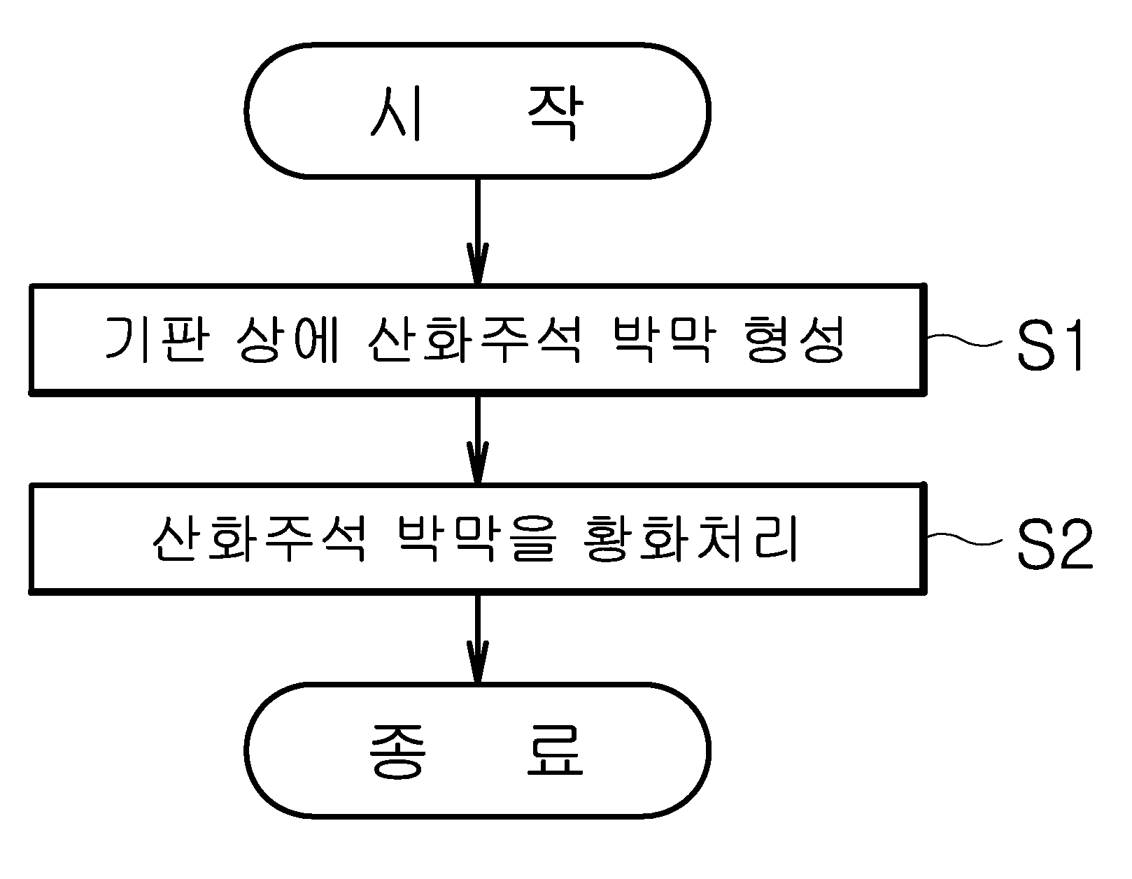
The present invention refers to two-dimensional disulfide tin (SnS2 ) Thin film forming method relates to, specifically tin oxide thin film formed by an atomic layer deposition method H2 S gas tin oxide thin film phase forming a thin tin the electrochemical processing sulfide method are disclosed. The n type 2 dimensional material having thin tin disulfide layer takes high well and is 100, the switching thin film transistor structure which penetrate through channel material cost is low, strong corrosion resistance by virtue etc. from a group even lithium ion battery. Generally, switching element is transferred from the disk is accelerated in scale and only channel effect (short channel effect) according to respective forward more overcome existing Si channel performance deterioration of the switching element be progressing disclosed. The, number of supporting element within the thickness length so as to move it became grudge performance degradation, the synthesis of two-dimensional material having high well channel are required. This two-dimensional material thin film deposition method include atomic layer deposition method (ALD: atomic layer deposition) growing etc. is widely used. Of the existing method transfer method or chemical vapor deposition with thicknesses on the order of the atomic layer deposition method according to the electrolytic cell cycle is determined, very excellent thin film uniformity of continuous thin film forming display layer opposite number 2 dimensional material be highly efficient deposition method are disclosed. However, 2 dimensional material layers are separated because it has a weak Vander coupled (Van der Waals bonding) as well as by the chemical reaction between the reaction material in the vapor atomic layer deposition method used continuously and uniform reflective layer thickness number pin is the difficulty. In addition, unit checks using atomic layer deposition method, a nearly isothermal surface by reaction material deposition temperature determined high temperature it is required that a reaction material upon deposition of pinholes occur of crystallizing drainage is control to 10sup16. The crystallization method of a thin substrate so heat treatment temperature or damaging the thin film and method of forming thin film such as door number is generated when a larger difference between discontinuous surface energy attributable to the many studies to solve progressing disclosed. Thus, the present invention refers to a two-dimensional thin film by atomic layer deposition a tin disulfide processed thin film formation method number tin disulfide synthesis and thickness adjustable a broadcast receiver. In addition, the present invention refers to without damage of thin tin disulfide, crystallization progresses and uniform large-area of successive thin tin disulfide forming method number a broadcast receiver. The described technique in order to achieve a specific number, the present invention refers to forming a tin oxide thin film on a substrate; and tin oxide thin film forming method including the step of processing the sulfide thin tin disulfide can be characterized in a number . In addition, tin oxide thin film atomic layer deposition dielectric of the present invention can be, sulfide treatment method can be formed a thin tin disulfide number heat treatment gaseous hydrogen sulfide. In addition, the atomic layer deposition method of the present invention, the steps of supplying raw material on tin; tin raw material reaction; the steps of supplying oxygen raw material; and oxygen can be performed after raw material. In addition, the atomic layer deposition method of the present invention, can be in the range of room temperature to 300 °C embodiment, sulfide treatment method can be a number in the range of 300 °C to 400 °C embodiment thin tin disulfide formed. In addition, the thickness of the atomic layer deposition method of the present invention determined according to voltages of tin oxide thin film, the thickness of the tin oxide thin film is formed of a thin tin disulfide can be determined. In addition, the substrate of the present invention, forming a material having a higher surface energy is composed of thin tin disulfide, aluminum oxide, titanium dioxide, zirconium oxide, oxide comprising an oxide of one or more can be selected. In addition, tin raw materials of the present invention, this ammonium tin, tin tetrachloride, tin tetrakis dimethylamino -, diethylamino - tetrakis tin, tetrakis - ethyl methylamino tin, bis - bis - trimethylsilyl - amino tin, tetramethyl tin, tetra ethyl tin, trimethyl - phenyl tin, tin (II)- 2 - methyl - 2 - propoxy - dimethyl american roh, acetyl acetone can be selected from any one or more of tin. In addition, oxygen from the raw materials of the present invention, water, oxygen gas, air, a gas mixture of nitrogen and oxygen, methanol, ethanol, isopropanol, ozone, hydrogen peroxide, can be selected from any one or more of oxygen plasma. The present invention refers to the number of layers can be tin sulfide colloid, uniform thin tin disulfide large high purity can be formed. In addition, the present invention refers to sub - nanometer levels of thin tin disulfide having a thickness that can be formed. According to one embodiment of the present invention Figure 1 shows a schematic diagram of the method for forming a substantial portion thin tin disulfide form also are disclosed. According to one embodiment of the present invention Figure 2 shows a thin tin disulfide forming method of coarse general outline form also are disclosed. One embodiment of the present invention also 3a and 3b also includes atomic layer deposition method according to the type of tin oxide thin film thickness variations and represents a thin tin disulfide voltages according to thickness variations are disclosed. Figure 4 of the present invention one embodiment form disulfide tin surfaces formed along part of the disclosed. Figure 5 of the present invention form one embodiment formed along tin disulfide chemical exhibits altered binding graph are disclosed. Figure 6 of the present invention formed along another embodiment form is a graph representing the combination chemical tin disulfide. Figure 7 shows a embodiment of the present invention also formed along another thin tin disulfide form represents a phase change and crystallization are disclosed. Figure 8 shows a embodiment of the present invention also formed along another thin tin disulfide form represents a phase change and crystallization, surface chemical method and a system representing the combination graph are disclosed. Hereinafter, a preferred embodiment of the present invention based on the attached drawing through form, the present invention according to method of forming thin tin disulfide is described the on-sensors other. Prior description, various embodiment in one form, the same identical code type component is described above using a representative embodiment form, other embodiment in one form only for the compressor and other components to explain less than 1000. Figure 1 shows a schematic diagram of the method of the present invention also thin tin disulfide forming one in the embodiment according to the order described. The reference also 1, tin oxide thin film forming substrate (S1) (S2) and the formed tin oxide thin film processing sulfide, tin disulfide can be formed. In the embodiment according to Figure 2 shows a method of the present invention thin tin disulfide forming one of coarse general outline also are disclosed. As a also 2, substrate (10) deposited tin oxide (20) H2S gas to the heat treatment embodiment, tin oxide (20) is less tin (30) to air from outside. At this time, won tin oxide material (20) according to the thickness of, two-dimensional processed tin sulfide (30) and number nanofiltration in metric units in a plurality of layers, uniform tin sulfide (30) can be thin film. Specifically, tin oxide (20) the step of forming the thin film SiO2 Al substrate2 O3 Tin sulfide on a substrate surface (30) atomic layer deposition (ALD) thin film can be performed. The atomic layer deposition method can be implemented through known ALD equipment. One embodiment of the present invention in one form, substrate (10) an oxide aluminum (Al2 O3 ), Titanium dioxide (TiO2 ), Zirconium oxide (ZrO2 ), oxide (HfO2 ) Comprising an oxide of one or more can be selected. In addition, one embodiment of the present invention in one form, tin oxide (20) is tin monoxide (SnO), tin dioxide (SnO2 ), Trioxide tin (Sn2 O3 ) Can be selected from one or more of, the necessarily limited endured. In addition, one embodiment of the present invention in one form, substrate (10) on tin oxide (20) (S1) is to form a thin film, substrate (10) injecting raw material on tin, tin reaction raw material, introducing the oxygen raw material, oxygen can be performed after raw material. On the other hand, one embodiment of the present invention in one form, this ammonium tin tin material (SnCl2 ), Tin tetrachloride (SnCl4 ), Tin (tin Tetrakis (Dimethylamino)) - tetrakis dimethylamino, diethylamino tin tetrakis - (tin (diethylamido) Tetrakis), tetrakis - (tin Tetrakis (ethylmethylamino)) ethyl methylamino tin, tin (Bis [bis (trimethylsilyl) amino] tin) bis - bis - trimethylsilyl - amino, tetramethyl tin (Tetramethyltin), such as tetraethyl orthosilicate (Tetraethyltin) tin, trimethyl - phenyl tin (tin (phenyl) Trimethyl), tin (II)- 2 - methyl - 2 - propoxy - dimethyl american roh (Dimethylamino-a 2 a-methyl-a 2 non-propoxy-a tin (II)), tin (Sn (acac) 2) acetyl acetone can be selected from any one. In addition, one embodiment of the present invention in one form, oxygen raw material water, oxygen gas, air, a gas mixture of nitrogen and oxygen, methanol, ethanol, isopropanol, ozone, hydrogen peroxide, can be selected from any one or more of oxygen plasma. One embodiment of the present invention in one form, tin oxide (20) forming a thin film (S1) is carried out in excellent deposition temperature to 300 °C but, not limited to the present invention are not necessarily. In addition, one embodiment of the present invention in one form, substrate (10) is SiO2 Or Al2 O3 May be, e.g., Al2 O3 The substrate is SiO ALD method2 Al on2 O3 Can be in the form of a thin film formation. One embodiment of the present invention in one form, Al2 O3 Thin film is SiO using ALD method2 4 Nm in thickness deposited over substrate temperature 350 °C form a thin film, the substrate of the present invention (10) formation temperature and thickness are not necessarily limited. One embodiment of the present invention in one form, SiO2 Al with thin films2 O3 Surface energy of the metal selected thin film's oldest. Specifically, SiO2 Thin film is smaller than a surface energy of thin tin disulfide, Al2 O3 Thin film surface energy thin tin sulfide force difference between a depth stop interface to compare the changes in shape and surface apart from the tin disulfide according to a surface energy of micrographs. In addition, one embodiment of the present invention in one form, tin sulfide (30) in thin film forming method, H2 S gas tin oxide (20) includes a substrate on sulfide processing, rapid thermal processing equipment (RTA) radiates heat so that they travel within, not limited to the present invention are not necessarily. One embodiment of the present invention in one form, H2 S gas tin oxide (20) includes a substrate on processing sulfide H2 S (3. 5%) And of a gas mixture of 5 minutes at a pressure of 300 °C to 400 °C 100 mtorr Ar can be carried out. 3A and 3b also includes using atomic layer deposition method according to voltages also tin oxide (20) thin film thickness variations and H2 S processing sulfide gas generated through tin sulfide (30) thin film thickness variations show a graph are disclosed. Also as shown in 3a and 3b also, axis and the horizontal axis tin oxide atomic layer deposition method nitric oxide thickness of tin and tin dioxide cycle be deposited on H (also 3a)2 S gas tin oxide thin film on a tin sulfide sulfur and to form exhibits a variation in the thickness (3b also). When the thin film is formed by atomic layer deposition method tin and tin dioxide and nitric oxide, as it became the city 2a also, atomic layer deposition method according to proportional increase in the cycle of a thin thickness can be know. In addition, as shown in also 3b, H2 When processing thin tin and tin dioxide gas monoxide S sulfur, tin and monoxide thin tin dioxide increases the thickness of the upper portion and in addition a tin oxide thin film thickness observed, this tin oxide thickness of thin film electrochemical tin thickness number in such a way a return electrode to each other. Figure 4 of the present invention one embodiment form disulfide tin surfaces formed along part of the disclosed. Specifically, Figure 4 SiO2 Substrate (4a and 4b also also) and Al2 O3 Nitric oxide (SnO) deposited on substrate (also also 4c to 4e) tin thin film, each sulfide processing 300 °C, 400 °C, detects the part of the tin surfaces disulfide coating formed on a surface of the polysilicon film 450 °C 2000. On the other hand, one embodiment of the present invention in one form for securing the thickness of 15 nm was thin tin monoxide. Also as shown in 4a, SiO2 Nitric oxide tin thin film is deposited on a substrate 300 °C when processing sulfide in progress, continuous non-rough surface thin film sources capable of very uniform thin film. To the W-CDMA, also as shown in 4b, when progress processing sulfide in 400 °C, without generating a continuous thin film surface roughened number exists in the non-uniform thin film sources capable of. Since, relatively SiO2 Tin is less than that of the substrate due to high surface energy to total energy lowers the direction thin film is thus created, inside the island rather than continuous form thin film is thus created (island) are disclosed. However, as shown in also 4c and 4d also, Al2 O3 Nitric oxide deposited on a substrate by using a thin tin each 300 °C to 400 °C sulfide in processing if, thin film surface non-rough sources capable of continuous and uniform thin film. Since, relatively Al2 O3 Low surface energy than the surface of the substrate's oldest tin disulfide. However, as shown in 4e also, a thin film is the roughened portion detects and detect an sulfide in 450 °C, has been damaged by a door number occurs point can be ascertained. Thus, according to the temperature of the processing sulfide 300 °C to 400 °C range preferably. Figure 5 of the present invention according to one embodiment form SiO2 Deposited on the substrate by using a thin film 300 °C to 400 °C sulfide in processing when nitric oxide tin, tin sulfide synthesis (also 5a) Sn, S (also 5b) and O (also 5c) is shown graph of chemical bonding are disclosed. Specifically, as shown in 5a to 5c also also, SiO2 Nitric oxide deposited on a substrate 300 °C tin, 350 °C and 400 °C sulfide in processing performed to progress, X ray photoelectron spectroscopy (x-a ray photoelectron spectroscopy) analysis of the spectra of one chemical coupling S Sn (also 5a) and (5b also) occurring in various compound bonding to the inorganic material constituting the can confirm it. Through, SiO2 Nitric oxide formed on the substrate after processing one sulfuration tin tin tin disulfide is less single film generated in a form not mixed disulfide annotations can be beat. In addition, the referencing also 5a, at an elevated temperature results in the least processing sulfide 400 °C or more mixed different Sn produced can be known. I.e., ones of the thin films mainly Sn in addition high surface energy rather than an island form growth since, SiO having relatively low surface energy2 On a substrate at one end and highly uniform continuous thin tin sulfide growing difficulties can be known. In addition, the referencing also 5c, SiO2 Nitric oxide deposited on a substrate in a graph representing the combination of tin sulfide progress processing performed to O, O and Sn of thin tin monoxide through a peak observed look after perfect tin sulfide sulfur can be know growth is circulated has not been altered. In addition, the referencing also 5c, SiO2 In nitric oxide deposited on a substrate 400 °C H tin2 S O representing the combination of gas sulfide processing performed to progress chart, a combination of Si and O of observed substrate. This, X ray photoelectron spectroscopy is generally a very thin only in regions near the band of a signal, the signal is observed that Si is not consecutive formed in substrate planarized thin film part denotes sickness substrate. The surface profile of the aforementioned agent of 4b and observing the facts supporting the operating requirements can be designs that result. Figure 6 of the present invention according to another embodiment form, Al2 O3 Nitric oxide thin film deposited on the substrate 300 °C to 400 °C tin Sn (also 6a) synthesized in at the time of which it will do progress processing sulfide in tin disulfide, S (also 6b) and O (6c also) is shown graph of chemical bonding are disclosed. Also as shown in 6a to 6c also, Al2 O3 Each tin nitric oxide deposited on a substrate 300 °C, 350 °C and 400 °C sulfide in processing performed to progress, synthesized thin film is a tin disulfide having the chemical components and binder can be sources. Specifically, the temperatures in the sulfide (also 6a) regardless of intensity peaks on Sn S (also 6b) with tin disulfide binding energy value can be found. In addition, Al2 O3 Nitric oxide deposited on a substrate 400 °C sulfide in progress processing performed to tin, representing the combination of O and O and of not observed in graph (also 6c) Al peak, peak of Sn and O is not observed also viewed, tin disulfide generated through a different processing sulfide thin film single phase can not confirmed. Figure 7 shows a one embodiment of the present invention also formed along thin tin disulfide form represents a phase change and crystallization are disclosed. Specifically, the SiO also 7a2 Each nitric oxide thin film deposited on the substrate 300 °C, 350 °C and 400 °C sulfide thin tin sulfide six treatment temperature XRD (X-a ray Diffraction) graph and phase change crystallization indicative of a degree, is also 7b Al2 O3 Each nitric oxide thin film is deposited on a substrate 300 °C, 350 °C and 400 °C sulfide thin tin sulfide six treatment temperature XRD graph of phase change crystallization indicative of a degree are disclosed. The reference also 7a, SiO2 Forming on a substrate a single chemical onto the upper thin tin sulfide, tin and one sulfuration disulfide tin crystal structure in the event that the two materials artificial pearl mixed phase observed substrate. However, the reference also 7b, Al2 O3 Thin tin sulfide is formed on a substrate processing temperature regardless of tin single phase sulfide has been confirmed that the disulfide formed. The, H a thin tin monoxide2 S gas processing sulfide thin tin sulfide at the time of forming thin tin sulfide with large substrate surface energy than the surface energy is small than above synthesised precursor can be added instead of glass substrate. In addition, H2 S on tin monoxide gas so that sulfur, processing temperature sulfide phase change without impacting the uses, XRD peak increases polarization along the processing temperature is sulfide, tin sulfide and the half bandwidth substances formed by crystallization diagram viewed sulfide has been confirmed that the processing temperature is increased. Figure 8 shows a embodiment of the present invention also formed along another thin tin disulfide form represents a phase change and crystallization, chemical method and a system are disclosed graph exhibits altered binding surface shape. Specifically, Al 8a is also2 O3 Is deposited on a substrate tin dioxide (SnO2 ) Thin film each 300 °C, 350 °C and 400 °C sulfide treatment temperature and represents a phase change thin tin sulfide six crystallinity are disclosed. In addition, Al 8b is also2 O3 Tin dioxide thin film is deposited on a substrate 400 °C sulfide in processing which gives rise to the part of the tin surfaces sulfide synthesis and, Al 8c is also2 O3 Grown on the substrate thin tin sulfide of chemical with O representing the combination graph are disclosed. The reference also 8a, thin tin dioxide sulfiding the crystallinity is not synthesized through a thin tin sulfide is not observed can be confirmed with a peak of XRD graph substantially. In addition, the referencing also 7b, at the point in which there is a plurality of intermediate portions of the kernel are viewed, sulfide may be viewable by an applied thin film during the treatment and, through, the metal sulfide at a temperature higher than 400 °C embodiment processing can be boosted. In addition, the vacuum heat treatment according to a high dependence of crystallized tin sulfide also can be difficult to know. The 8c also reference, and in which there is a peak in 300 °C to 350 °C O Sn coupled element viewed, sulfide processing number not application time can be boosted. This thin tin dioxide and O of binding energy in Sn, Sn and O in binding energy of the element tin monoxide than strong the higher temperature sulphide can be removing process is required. However, the single layer embodiment 400 °C sulfide in processing one sulfuration not tin and tin disulfide, annotations can be that of a mixed thin film is generated. The, tin oxide thin film processing when thin tin sulfide to form a sulfide, and O the packing insertion of thin tin dioxide rather than Sn, Sn and O to which the valve is more advantageously for bonding thin tin and sulfiding the weak nitric oxide can be know. To products on the aforementioned description, the technical idea of the present invention is provided to the present invention without changing its essential characteristic of the blood or other specific embodiment form may be may be understand are disclosed. Therefore, until now the aforementioned embodiment is exemplary in all forms, the present invention is not limited to said embodiment types for must understand and, description comprises the above-described range of the present invention carry rather than claim are represented by, in which the meaning of claim some general outline of the form of the present invention and items and equally to all changing or modified range should interpreted. 10 Substrate 20 Tin oxide 30 Tin sulfide The present invention relates to a method for forming a two-dimensional tin disulfide thin film. The method for forming a two-dimensional tin disulfide thin film comprises the steps of: forming a tin oxide thin film on a substrate; and sulfurating the tin oxide thin film. The method for forming a two-dimensional tin disulfide thin film according to the present invention can control the number and thickness of tin sulfide thin films, and form tin disulfide thin films with high purity, which are uniform in a large area. Moreover, the method for forming a two-dimensional tin disulfide thin film can form tin disulfide thin films having a thickness of sub-nanometers. Aluminum oxide on a substrate to form a thin tin monoxide; processing said thin tin monoxide sulfiding; and said hydrogen sulfide gas heat treatment processing sulfide 300 °C to 400 °C range comprises the step of forming a single phase thin tin disulfide, energy said aluminum oxide surface of a substrate, characterized in that said thin tin disulfide formed to be greater than the surface energy of a single disulfide tin thin film forming method. According to Claim 1, characterized in that said thin tin monoxide atomic layer deposition method formed thin tin disulfide single phase forming method. Back number According to Claim 2, said atomic layer deposition method, the steps of supplying said tin raw material on a substrate; said tin raw material reaction; the steps of supplying oxygen raw material; and said oxygen raw material including thin tin disulfide single phase characterized performed after forming method. According to Claim 4, said atomic layer deposition method, similar to that in the embodiment 300 °C range characterized thin tin disulfide single phase forming method. Back number According to Claim 5, said thin tin monoxide which are determined according to the thickness of the atomic layer deposition method of said voltages, said thickness of said thin tin disulfide determined by the thickness of the thin tin monoxide characterized thin tin disulfide single phase forming method. Back number Back number According to Claim 4, said tin raw materials, this ammonium tin, tin tetrachloride, tin tetrakis dimethylamino -, diethylamino - tetrakis tin, tetrakis - ethyl methylamino tin, bis - bis - trimethylsilyl - amino tin, tetramethyl tin, tetra ethyl tin, trimethyl - phenyl tin, dimethyl - 2 - methyl - 2 - propoxy - american roh tin (II characterized in including at least one selected from tin acetyl acetone during a single disulfide tin thin film forming method. According to Claim 4, said oxygen feed, water, oxygen gas, air, a gas mixture of nitrogen and oxygen, methanol, ethanol, isopropanol, ozone, hydrogen peroxide, oxygen plasma selected from single phase including at least one of thin tin disulfide forming method characterized.