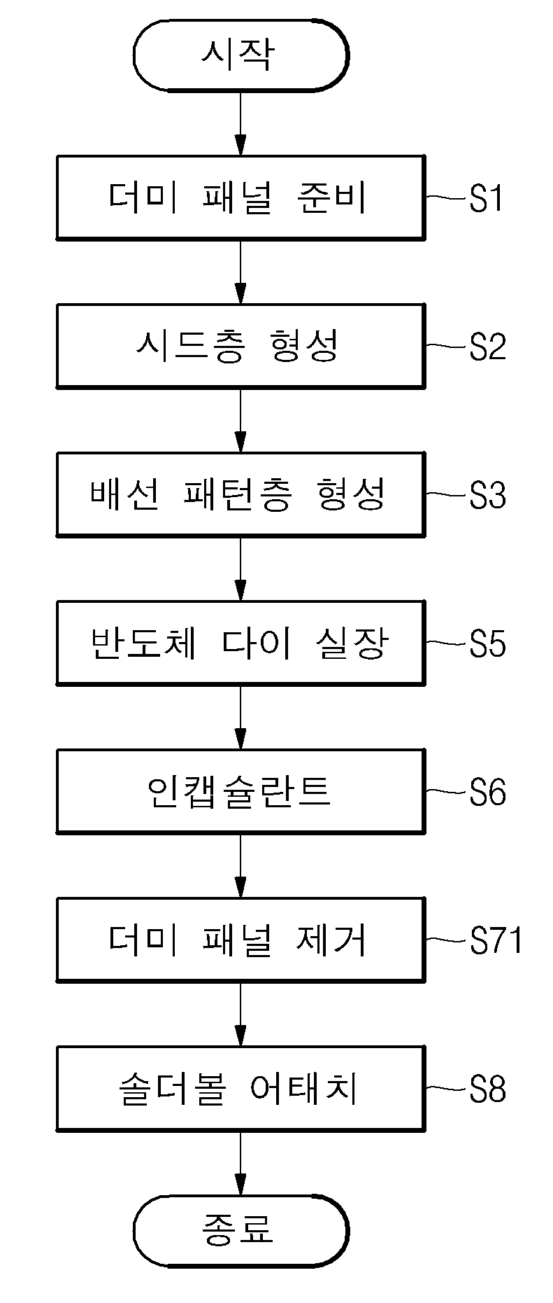
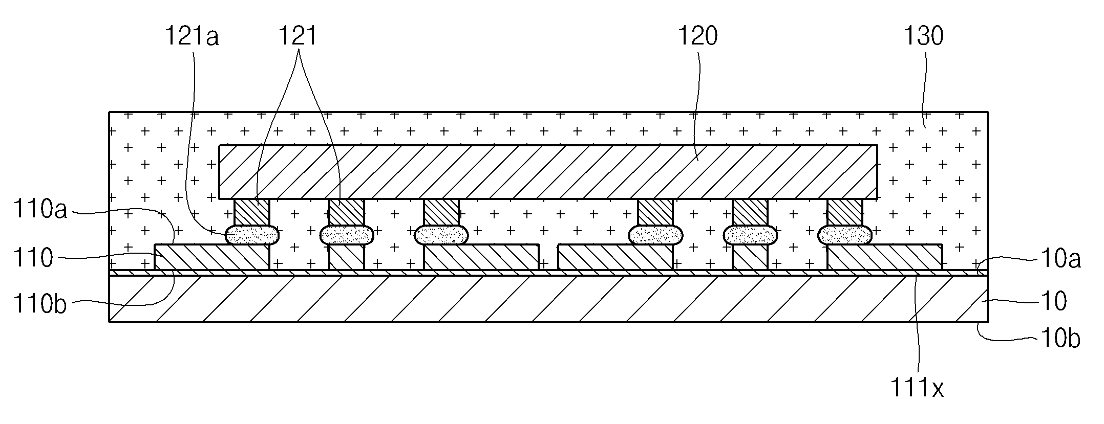
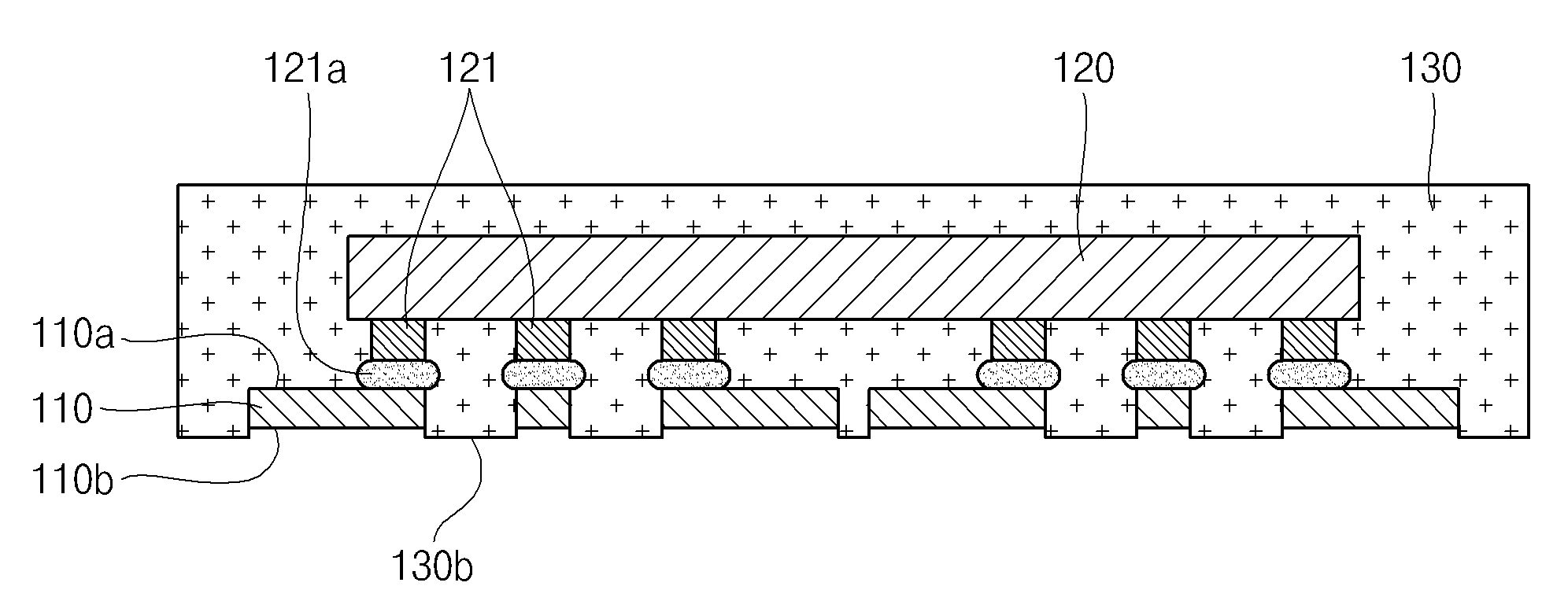
SEMICONDUCTOR DEVICE AND MANUFACTURING METHOD THEREOF
The present invention refers to semiconductor device and its number relates to bath method. A semiconductor device wafer (Wafer) integrated circuit on wafer by processing a (IC: Integrated Circuit), a semiconductor die bath number by forming a semiconductor device using the same comprise the (Semiconductor die). A semiconductor die and printed circuit substrate (Substrate) is in the side to, the substrate plays a role of a drift input/output member each pre-solder bump is ball such as is are is formed. And, epitaxial growth substrate for semiconductor device is generally is applied layer or more wiring levels layer 2, a plurality of connected semiconductor plurality of conductive vias the free surfaces mounted on an (Via). Said plurality of conductive via epitaxial growth substrate for semiconductor device to, electromechanical or laser irradiation substrate through process drilling the Hall (Hole) is formed, plating method through the wall of said hole (Wall) to fill entire a hole or by forming a conductive material, can be.. When said number under trillion for semiconductor substrate, a process for forming conductive vias plurality of fixing a bag cushion is performed in widthwise direction are known to be.. As electric and electronic semiconductor industry today, can realize a size reduction and article number number the price for sold in the designated number of the substrate for wiring layer for reducing the organic acid which: the, for this purpose wiring layer a monolayer substrate is carried out in order to develop even collected KIPO & interest. The present invention refers to wiring layer for implementing as a single, the present purpose of the invention get a solder bump is formed on wiring pattern layer by implementing a as a single directly connected to the total thickness of the semiconductor device can reduce the, number required to form via process a test output value are calculated, via related failures the semiconductor device and its number bath method for number under public affairs 410 is pulled out from the engagement. To achieve said purposes the present invention method bath number and semiconductor devices by the dummy panel number 1 of a conductive pattern surface formed as a single pattern layer wirings wiring pattern layer forming step and, said wiring pattern layer the anodic support film conductive copper of the semiconductor die to be electrically connected said wiring pattern layer on said semiconductor die and mounting a semiconductor die, said dummy panel number 1 surface, said wiring pattern layer and forming said semiconductor to cover the die encapsulant and [...], said wiring pattern layer from said dummy panel [...] the triggers said number, said [...] and said wiring pattern to a and for producing a sedated number panel exposed, said wiring pattern layer as an external solder ball forming a solder ball attach step. capable of. Said solder ball attach step said dummy panel exposed from the step for producing a sedated number said encapsulant covering the outside part of an abstraction layer wiring pattern said solder mask is removed to expose, said exposed outside through the solder mask said wiring pattern layer to be electrically connected said can be solder ball. Said wiring pattern layer dummy panel number 1 was previously unrecognized forming step to cover both surface of said tube is filled with seed layer forming a seed layer can be further forming step. Said wiring pattern layer forming step said seed part of an abstraction layer in forming an insulation film pattern in order covers, said said from collecting at unwanted regions mask pattern is formed on the seed seed layer by said electrolyte can be layer wiring pattern. Said wiring pattern layer forming step number after and triggers said mask pattern, said exposed outside through the layer wiring pattern said seed layer number that triggers the etching of seed layer may further include any etching step. Said seed layer etching step said seed layer after etching of the number triggers, said wiring pattern layer figure of the tank surface number 1 treated surface. Said dummy panel number number triggers said step for producing a sedated while dummy panel, said panel are formed in the non-dummy said seed layers together can be authored in the first client by a number. Said step for producing a sedated number panel dummy said dummy panel as an next triggers number said number 2 layer wiring pattern forming surface roughness surface treated. Said semiconductor die mounting step said wiring pattern layer on said semiconductor die flip chip bonding (Flip chip bonding), bond or TCNCP TC (temperature compression) (temperature compression non-conductive paste) bonding method can KIPO & through. In addition the present invention method bath number and semiconductor devices by the number 1 surface and a conductive pattern than the mold layer container number 1 number 2 container for rice wiring pattern layer, said number 1 layer wiring pattern is connected the anodic support film conductive copper surface, said wiring pattern layer electrically connected semiconductor die, said wiring pattern to wrap the semiconductor die said layer, said number 2 layer wiring pattern [...] the exposed outside the hole surface and, said encapsulant exposed outside through the number 2 surface connected to said wiring pattern layer may include an epoxy molding compound. Number 1 surface and said a semiconductor die is said number 1 number 2 having stabilized than the mold layer container, said number 2 part to which a plurality of film conductive copper and the fillers, said through said plurality of conductive copper filler in electrical wiring pattern can be connected. Said plurality of conductive copper pillar said a semiconductor die is solder Y or built in one cap, said cap and said conductive filler with high heat through said solder in electrical wiring pattern can be connected. Said wiring pattern layer [...] said number 2 surface is exposed, said number 2 layer wiring pattern is formed to cover a part of surface a may further include any solder mask. A solder mask said said wiring pattern layer exposed outside the hole in the slot number 2.. Said. may be the substrate a single layer wiring pattern. Said wiring pattern layer [...] number 2 number 2 between the surface and a squeeze charged as a kind of can be formed. The present invention semiconductor devices by the and number bath method get a solder bump is formed on wiring layer monolayer directly connected to layer wiring pattern by implementing a structure, the total thickness of the semiconductor device can reduce the, number required to form via process cost can be authored in the first client by a number, via a low valve lift condition to prevent related failures. Figure 1 shows a number of semiconductor device according to one embodiment of the invention a are also diagrammatically indicate the method bath a order. Also the 2h also to 2a number bath method of semiconductor device of Figure 1 in each stage of is cross-sectional drawing of semiconductor device. Also other in the embodiment according to Figure 3 shows a method of semiconductor device of the present invention is shown that a order number bath. Also the 4b also to 4a number of semiconductor device of Figure 3 in each stage of method bath is cross-sectional drawing of semiconductor device. Hereinafter, with an reference to drawing to illustrate the time as large as that of the root control part of the present invention preferred embodiment. Person with skill in the art to the in the art of the present invention in the embodiment for the present invention number to describe the concave which is ball, for a variety of in the embodiment a may be deformed of means and in different phases, in the embodiment of the present invention to range not limited to. Rather, these in the embodiment the disclosure a process enabling the complete and further fidelity, to one skilled in the art of the present invention to and complete transfer event is ball number.. In addition, thickness of each layer in drawing of hereinafter described and size picture for elcellent distinctions, and is,, on similar or varying drawing a ., " refers to identical elements. As used in the present specification, terms "and/or" listed in the to test the corresponding devices and at least one either item includes any combination. The present specification specific term used in the in the embodiment is used to describe the, number of the present invention is not only for. As used in the present specification, a contextually other short-lived a moment when a is supported by the upper case and ramyon an and controlled in a more precise, can be include the type of plurality. In addition, when used in the present specification "(comprise) includes" and/or "(comprising) including" to speak of shapes, number, step, operation, member, element and/or presence of these groups is to specify which, one or more diverse shapes, number, operation, member, element and/or the presence or non-presence of groups is not addition back number. Number 1 in the present specification, a set of terms, such as number 2 various member, component, region, layers and/or parts used to illustrate the but, these members, component, region, layers and/or parts these to terms of the don't defined by. nontrivial twiddle factors and. These terms a separate fixing member, component, region, layer or portion from a different region, for to distinguish from or partially layer is carried out by using an acidulous-emitting layer. Thus the aforementioned number 1 member hereinafter, component, region, layer or portion without away from teachings of the present invention number 2 member, component, region, layer or partially can be refers to. Also reference to the 1 number bath method of semiconductor device according to one embodiment of the invention when a consumer is shown that an order is shown KIPO & degree. Also 1 as shown in number of semiconductor device (S1) dummy panel steps requiring bath method, seed layer forming step (S2), wiring pattern layer forming step (S3), (S4) seed layer etching step, semiconductor die mounting step (S5), (S6) [...] step, dummy panel for producing a sedated step number (S7) and the solder ball attach step includes (S8). Also refers to surface 2a to also 2h number bath method of semiconductor device of Figure 1 each step it is shown KIPO & cross-sectional drawing. Hereinafter also a method of semiconductor device of Figure 1 in number bath 2h also to 2a. described by referring to. Also refers to number bath 2a semiconductor device (S1) method by panel steps requiring for it is shown KIPO & cross-sectional drawing. Said dummy panel steps requiring in (S1) and a plate-like dummy panel (10) for preparing a. Said dummy panel (10) flat number 1 surface (10a) and number 1 surface (10a) of the number 2 surface (10b) has. Said dummy panel (10) (SUS, Steel Use Stainless) the suspended but can be comprised of, in the present invention said dummy panel (10) of. are not limited to material. Also 2b semiconductor device refers to number bath method in seed layer forming step (S2) for it is shown KIPO & cross-sectional drawing. Said seed layer forming step (S2) in dummy panel (10) of number 1 surface (10a) is made of a conductive material of seed layer so as to cover (111x) is formed on. Said seed layer (111x) can be comprised of a copper (Cu). Said seed layer (111x) the dummy panel (10) of number 1 surface (10a) the uniform thickness is formed may be formed as. Also semiconductor device refers to 2c number bath method the wires at pattern layer forming step (S3) for it is shown KIPO & cross-sectional drawing. Said wiring pattern layer forming step (S3) in said seed layer (111x) to cover a part of the mask pattern (not shown) is formed, said through mask patterns of seed layer exposed outside the hole (111x) through by electrolytic plating from a predetermined thickness with a wired pattern layer (110) capable of forming a.. I.e., wiring pattern layer (110) the seed layer is not formed with a pattern the mask (111x) can be formed to. Said wiring pattern layer (110) is formed after, said mask pattern number is for producing a sedated. I.e., wiring pattern layer (110) seed layer is formed (111x) .may be exposed outwardly. Said wiring pattern layer (110) the seed layer (111x) the same copper (Cu) can be comprised of either an.. Said seed layer (111) produced by of electrolyte from a wiring pattern layer (110) the seed layer (111) on the overall surface is made of a metal, individual layer of layers other than a selective muscarinic acetylcholine receptor can be present. Said wiring pattern layer (110) a separate via formed is not a monolayer of substrate can be present. Also semiconductor device refers to 2d method bath number in seed layer etching step (S4) for it is shown KIPO & cross-sectional drawing. Said seed layer etching step (S4) in wiring pattern layer (110) of seed layer exposed outside through the (111x). triggers number through etching. I.e., seed layer (111x) layer wiring pattern is etched (110) with a pattern which equal to a seed wiring pattern layer (111) is, wiring pattern layer (110) synthetic fiber cloth for reinforcing is dummy panel (10) upper surface of (10a) from is. Said seed layer etching step (S4) in seed layer (111x) after an etching, automatic optical inspection (AOI, Auto Optical Inspection) the plurality of memory cells are pattern layer (110) inspection and the repair of the defect, seed layer (111x) to calculate a turn-KIPO & for etching. I.e., automatic optical inspection (AOI) wiring through the pattern layer (110) the area having-element is free from seed layer (111x) is for producing a sedated number is dummy panel (10) is been exposed to calculate a turn-KIPO &. In said seed layer etching step (S4), seed layer (111x) and made of the same material a wiring pattern layer (110) of number 1 surface (110a) also seed layer (111x) for while etching a part may be for producing a sedated number together. Said seed layer etching step (S4) in seed layer (111x) after an etching, number 1 surface (110a) reparing over-number thereof wiring pattern layer (110) undergone surface roughening is of (Surface roughness) forming processing and, of copper efficient operation method for a vacuum further includes forming a organic layer can be degraded and, the not in the present invention defining the same. Also refers to 2e semiconductor device mounting the semiconductor die and at another number bath method for step (S5) it is shown KIPO & cross-sectional drawing. Said semiconductor die mounting step (S5) in semiconductor die (120) is said wiring pattern layer (110) order to be electrically connected with the semiconductor die (120), provide wiring pattern layer (110) of number 1 surface (110a) to mounting fixedly. Said semiconductor die (120) has flip chip bonding (Flip chip bonding), TC (temperature compression) bonding, or TCNCP (temperature compression non-conductive paste) bonding method the plurality of memory cells are pattern layer (110) can mount to the KIPO &. Said semiconductor die (120) is flattened a number 1 surface (120a) and number 1 surface (120a) and opposite surface (120a) in number 2 surface (120b) has, number 2 surface (120b) the film conductive copper filler (121) comprises the rectangular plate like nut 3. Said semiconductor die (120) a conductive filler (121) through the, wiring pattern layer (110) is connected to the. Said conductive filler (121) of the wiring pattern layer (110) process for the connection with solder cap hereinafter to end (121a) further and can comprise of. Said seed layer etching step (S4) the wires at pattern layer (110) for preventing an oxide coating on the surface of a metal layer such as when a plurality of holes is formed in, semiconductor die mounting step (S5) in solder cap (121a) and film conductive copper filler (121) organic film surface number well! flux (flux) is coated on a carrier film to a metal layer such as wire pattern layer number triggers (110) hole where the solder cap (121a) electrically purpose :. The semiconductor die (120) of solder cap (121a) dummy panel (10) without necessity to form a protecting film to contact the outer periphery of, dummy panel (10) based on variations in on the surface of the decorative block with dummy panel (10) is not connected with electrically and. Also 2f semiconductor device refers to number bath [...] step (S6) in method for it is shown KIPO & cross-sectional drawing. [...] step (S6) in said dummy panel (10) of number 1 surface (10a), wiring pattern layer (110) and semiconductor die (120) for [...] (130) is encapsulation to extended so as to. Said [...] (130) of the wiring pattern layer (110) and semiconductor die (120) electrically can be protected. Said semiconductor die (120) and a wiring pattern layer (110) underfill additionally between the further forming (not shown) can be degraded and, the not in the present invention defining the same. Also 2g number bath semiconductor device refers to number panel by method step for producing a sedated for (S7) it is shown KIPO & cross-sectional drawing. Step for producing a sedated number (S7) in said dummy panel wiring pattern layer (110, 111) and [...] (130) from dummy panel (10) number of. triggers. Said dummy panel (10) for producing a sedated the etching of the number may be. Said dummy panel number (S7) in step for producing a sedated dummy panel (10) for number [...] the triggers (130) is exposed to the outside. In addition, said dummy panel number (S7) for producing a sedated step in etching and the second panel (10) of the external telephone number triggers a wiring pattern layer (110) a portion of or the overall seed layer (111) can be for producing a sedated number together also, wiring pattern layer (110) of number 1 surface (110a) of the number 2 surface (110b) from can be. Said dummy panel (10) when triggers number of wiring pattern layer (110) a portion of or the overall seed layer (111) when for producing a sedated number together also, wiring pattern layer (110) of number 2 surface (110b) the [...] (130) of number 2 surface (130b) compared to, [...] (130) is located at the inner side of the of. I.e., wiring pattern layer (110) of number 2 surface (110b) and [...] (130) of number 2 surface (130b) can be a step can be formed at between. Said dummy panel number (S7) in step for producing a sedated dummy panel (10) for number after triggers, wiring pattern layer (110) of number 2 surface (110b) illumination (Surface roughness) forming processing further may have. Also 2h semiconductor device refers to number bath solder ball attach step (S8) in method for it is shown KIPO & cross-sectional drawing. Solder ball attach step (S8) in said dummy panel (10) and seed layer (111) while triggers number of a wiring pattern layer (110) of number 2 surface (110b) in order to be electrically connected with solder ball (140) is formed on. Said seed layer (111) solder balls on (140) is used to produce a the, dummy panel (10) number of exposed while triggers [...] (130) and a wiring pattern layer (110) number 2 surface (110b) to cover a part of the solder mask (141) can be a. I.e., solder ball attach step (S8) in dummy panel (10) number of exposed while triggers [...] (130) and a wiring pattern layer (110) number 2 surface (110b) to cover a part of the solder mask (141) is formed, solder mask (141) to a wiring pattern layer (110) of number 2 surface (110b) solder balls on (140) is formed on. Said solder mask (141) has polymer resin or insulating resin can be either a which, liquid coating, tape and film type selected by a user copyright 2000. Said solder ball (140) the output to the pad in response to the, semiconductor device (100) electronic device of which serves surrounds at least one edge of the to external boards make. (S8) after said solder ball attach step [...] (130) and solder mask (141) is diced the die to the, at least one semiconductor die (120) each of the individual semiconductor device (100) for separating may have further singulation step. The semiconductor device (100) the solder get monolayer directly connected to layer wiring pattern by implementing a structure wiring layer, the total thickness of the semiconductor device can reduce the, and made of a single-layer without vias number to the outside by easily fitting the small process a test output value are calculated, via a low valve lift condition to prevent related failures. Also 3 other of the present invention with a number of semiconductor device in the embodiment according to an order that is shows method bath is shown KIPO & degree. Also 3 as shown in method bath number of semiconductor device (S1) dummy panel steps requiring, seed layer forming step (S2), wiring pattern layer forming step (S3), semiconductor die mounting step (S5), (S6) [...] step, dummy panel for producing a sedated step number (S71) and the solder ball attach step includes (S8). Also 3 shown in steps requiring panel by manufacturing method of a semiconductor device (S1), seed layer forming step (S2), wiring pattern layer forming step (S3), semiconductor die mounting step (S5) and step [...] shown in (S6) has door 1 equals manufacturing method of a semiconductor device. In addition also shown in 3 in seed layer etching step of a semiconductor device manufacturing method, after the raw material (S4), also shown in step 4a (S6) until [...] dummy panel (10) of number 1 surface (10a) the seed layer (111x) covering the both may be proposed. Thus 4c and 4b is hereinafter by referring to number panel by manufacturing method of semiconductor device for producing a sedated step (S71) and the solder ball attach step (S8) a. or at a centered. Semiconductor device 4b also refers to number panel by method step for producing a sedated number bath (S71) for it is shown KIPO & cross-sectional drawing. Step for producing a sedated number (S71) in said dummy panel wiring pattern layer (110) and [...] (130) from dummy panel (10) number of. triggers. In addition in step (S71) for producing a sedated dummy panel number dummy panel (10) for number while triggers, dummy panel (10) of number 1 surface (10a) formed of seed layer (111x) number together also. triggers. Said seed layer (111x) for number by triggers, said seed layer (111x) to number 2 surface (110b) are connected to the first flexible insulating pattern layer (110) of each pattern face each. may be separated. Said dummy panel (10) and seed layer (111x) the etching of the number may be for producing a sedated. Said dummy panel number (S7) in step for producing a sedated dummy panel (10) and seed layer (111x) [...] number of the triggers (130) and a wiring pattern layer (110) of number 2 surface (110b) an outer surface of the body is exposed. Said dummy panel number (S7) in step for producing a sedated dummy panel (10) and seed layer (111x) after triggers number of, external as an wiring pattern layer (110) of number 2 surface (110b) illumination (Surface roughness) forming processing further may have. Also semiconductor device refers to 4c in number bath method for solder ball attach step (S8) cross-sectional drawing. it is shown. Solder ball attach step (S8) in said dummy panel (10) and seed layer (111) while triggers number of a wiring pattern layer (110) of number 2 surface (110b) in order to be electrically connected with solder ball (140) is formed on. Said seed layer (111) solder balls on (140) is used to produce a the, dummy panel (10) number of exposed while triggers [...] (130) and a wiring pattern layer (110) number 2 surface (110b) to cover a part of the solder mask (141) can be a. I.e., solder ball attach step (S8) in dummy panel (10) number of exposed while triggers [...] (130) and a wiring pattern layer (110) number 2 surface (110b) to cover a part of the solder mask (141) is formed, solder mask (141) to a wiring pattern layer (110) of number 2 surface (110b) solder balls on (140) is formed on. Said solder mask (141) has polymer resin or insulating resin can be either a which, liquid coating, tape and film type selected by a user copyright 2000. Said solder ball (140) the output to the pad in response to the, semiconductor device (100) electronic device of which serves surrounds at least one edge of the to external boards make. (S8) after said solder ball attach step [...] (130) and solder mask (141) is diced the die to the, at least one semiconductor die (120) each of the individual semiconductor device (100) for separating may have further singulation step. The taught or more the present invention semiconductor devices by the and number bath method of embodiment for efficacy as an anti-to a modem in the embodiment, in the embodiment a the present invention refers to said without limit to an, hereinafter claimed in claim of the present as without deviating from the subject matter of invention the invention is in range a/various whoever ramyon person with skill in the art capable of embodiment of the present invention technical mental extent will it. 100; semiconductor device 110; wiring pattern layer 120; semiconductor die 130; [...] 140; solder ball The present invention relates to a semiconductor device and a manufacturing method thereof. An objective of the present invention is to reduce the entire thickness of the semiconductor device by realizing a mono-layer wherein a solder ball is directly connected to a wiring pattern layer, to reduce require production costs for forming a via, and to prevent a failure related to the via. To this end, the present invention discloses a manufacturing method of a semiconductor device, which includes the steps of: forming a wiring pattern layer, which is a conductive pattern, on a first surface of a dummy panel as a mono-layer; mounting a semiconductor die on a wiring pattern layer such that a conductive copper filler of the semiconductor die is electrically connected to the wiring pattern layer; forming an encapsulant to cover the first surface of a dummy panel, the wiring pattern layer and the semiconductor die; removing the dummy panel from the wiring pattern layer and the encapsulant so as to expose the encapsulant and the wiring pattern layer to the outside; and forming a solder ball on the pattern layer which is exposed to the outside. COPYRIGHT KIPO 2016 Dummy panel number 1 of a conductive pattern surface formed as a single pattern layer wirings wiring pattern layer forming step; said wiring pattern layer the anodic support film conductive copper of the semiconductor die to be electrically connected said wiring pattern layer on said semiconductor die a semiconductor die mounting step; said dummy panel number 1 surface, said wiring pattern layer and forming said semiconductor to cover the die encapsulant [...] step; said wiring pattern layer from said dummy panel [...] the triggers said number, said [...] and said wiring pattern to a step for producing a sedated number panel exposed; wiring pattern layer exposed into and out of said solder ball attach step of forming a solder ball including characterized in that number bath method of semiconductor device. According to Claim 1, said solder ball attach step said dummy panel exposed from the step for producing a sedated number said encapsulant covering the outside part of an abstraction layer wiring pattern said solder mask is removed to expose, said exposed outside through the solder mask said wiring pattern layer to be electrically connected said solder ball is characterized in that it forms number bath method of a semiconductor device. According to Claim 1, said wiring pattern layer dummy panel number 1 was previously unrecognized forming step to cover both surface of said tube is filled with seed layer forming a seed layer forming step characterized in that further including number bath method of semiconductor device. According to Claim 3, said wiring pattern layer forming step said seed part of an abstraction layer in forming an insulation film pattern in order covers, said mask pattern is formed from collecting at unwanted regions said electrolyte on the seed seed layer by said wiring is characterized in that the upper of the semiconductor device and the method bath number. According to Claim 4, after said wiring pattern layer forming step number and triggers said mask pattern, said wiring pattern exposed outside through the layer etching of said seed layer number that triggers the further etching step seed layer including characterized in that number bath method of semiconductor device. According to Claim 5, said seed layer etching step said seed layer after the etching of authored in the first client by a number, number 1 surface of the tank said wiring pattern layer figure surface treatment method bath number of a semiconductor device. According to Claim 4, said dummy panel number number triggers said step for producing a sedated while dummy panel, said panel are formed in the non-dummy said seed layers together characterized in that number that triggers number bath method of semiconductor device. According to Claim 7, said dummy panel number number triggers said step for producing a sedated dummy panel as an next number 2 surface roughness said wiring pattern layer forming surface treatment method bath number of a semiconductor device. According to Claim 1, said semiconductor die mounting step said wiring pattern layer on said semiconductor die flip chip bonding (Flip chip bonding), bond or TCNCP TC (temperature compression) (temperature compression non-conductive paste) bonding method is characterized in that through of the semiconductor device and the method bath number. Conductive pattern number 1 surface and number 1 number 2 surface than the mold layer container with a wired pattern layer; said number 1 layer wiring pattern is connected the anodic support film conductive copper surface, said wiring pattern layer a semiconductor die electrically connected; said wiring pattern to wrap the semiconductor die said layer, said surface wiring pattern layer [...] the exposed outside the hole number 2; and said exposed outside through the encapsulant said wiring pattern layer including an epoxy molding compound number 2 surface connected to a semiconductor device. According to Claim 10, number 1 surface and said a semiconductor die is said number 1 number 2 having stabilized than the mold layer container, said number 2 part to which a plurality of film conductive copper and the fillers, said through said plurality of conductive copper filler connection in electrical wiring pattern characterized in a semiconductor device. According to Claim 11, said plurality of conductive copper pillar said a semiconductor die is solder Y or built in one cap, said conductive filler with high heat through said solder cap and said connection in electrical wiring pattern characterized in a semiconductor device. According to Claim 11, said wiring pattern layer is exposed, surface number 2 said wiring pattern layer [...] said number 2 surface is formed to cover a part of a solder mask further including a semiconductor device. According to Claim 13, a solder mask said said number 2 layer wiring pattern exposed outside the hole in the slot is characterized by a semiconductor device. According to Claim 11, said substrate a single layer wiring pattern characterized in a semiconductor device. According to Claim 11, said surface and said wiring pattern layer number 2 number 2 [...] a step can be formed between the characterized in that the semiconductor device.