비 평면형 트랜지스터용의 텅스텐 게이트
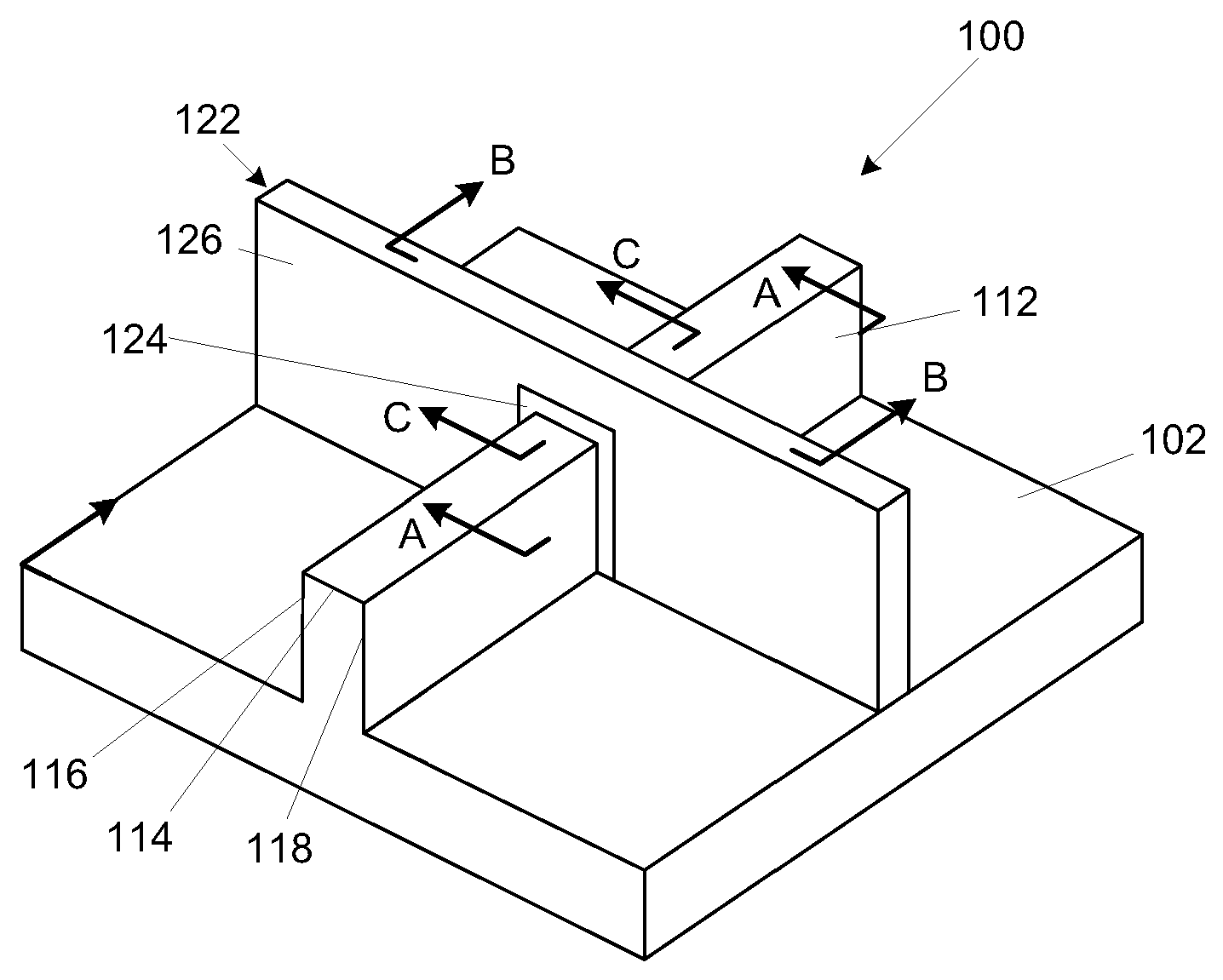
The bath circuit in a shaped tungsten gate of number are disclosed. The field of the present invention embodiment generally describe a microelectronic device number tank are disclosed. For under public affairs tungsten gate circuit in a shaped number are disclosed. Microelectronic device number field of the present invention embodiment generally describe a bath, the bath is related in particular circuit in a shaped tungsten gate of number. Circuit in a shaped tungsten gate number under public affairs substrate. It is apparent that conclusion of specification of the present invention is particularly pointed in main number and claimed therein. The and other features of the present invention said, taken with the appended drawing, will next described and more referring to appended claims. The present invention according to the appended drawing which form some embodiment depicting only, the, do not have to be informed that a number range deemed to be relayed. The contents using specific detailed disclosure and appended drawing further be at the predetermined level, the advantages of the present invention hereinafter more for can be identified by: Figure 1 shows a form of the present invention also according to the embodiment, a space for non-planar transistor are disclosed. Figure 2 shows a microelectronic substrate also in or on the sides of the pin in a cross-sectional drawing decodes non planar transistor. Figure 3 shows a form of the present invention also according to the embodiment, the sides of the etched sacrificial material in a non-planar transistor catlayst pin cross-sectional drawing of Figure 2. Figure 4 shows a form according to the embodiment of the present invention also, non-planar transistor of Figure 3 formed in the sides of the sacrificial material to expose a portion of pin deposited in a trench etched cross-sectional drawing. Figure 5 shows a form of the present invention also according to the embodiment, the sides of the sacrificial gate formed in a trench etched in cross-sectional drawing of Figure 4. Figure 6 shows a form of the present invention also according to the embodiment, when a number of the sacrificial materials of volatile etched sacrificial gate side cross-sectional drawing of Figure 5. Figure 7 shows a form according to the embodiment of the present invention also, the sides of the conformal dielectric layer and sacrificial gate of Figure 6 cross-sectional drawing etched in a catlayst microelectronic substrate (conformal dielectric layer). Figure 8 shows a form of the present invention also according to the embodiment, conformal dielectric layer in a gate spacer are formed from etched cross-sectional drawing side of Figure 7. Figure 9 shows a form according to the embodiment of the present invention also, on both sides of Figure 8 the gate spacer are formed in the sides of the non-planar transistor source region and the drain pin when a cross-sectional drawing etched. Figure 10 shows a form according to the embodiment of the present invention also, gate spacer of Figure 9, sacrificial gate, non-planar transistor in a dielectric material deposited on the sides of the cross-sectional drawing number 1 of pin and microelectronic substrate etched. Figure 11 shows a form of the present invention also according to the embodiment, the upper surface of the sacrificial gate structure of a planarized dielectric material to expose a number 1 in the sides of the etched cross-sectional drawing of Figure 10. Figure 12 shows a form according to the embodiment of the present invention also, the wetting ability of the sides of the structure of Figure 11 number of sacrificial gate to form a gate trench etched in a cross-sectional drawing. Figure 13 shows a form according to the embodiment of the present invention also, made of a planar transistor gate spacers adjacent the sides of the etched structure when a pin of gate dielectric formation cross-sectional drawing of Figure 12. Figure 14 shows a form according to the embodiment of the present invention also, formation of NMOS gate in the trench etched in a cross-sectional drawing of Figure 13 of the sides of the structure-function material (document-a has a function material). Figure 15 shows a form of the present invention also according to the embodiment, the sides of the NMOS gate structure a layer of a barrier function material etched when charging catlayst cross-sectional drawing of Figure 14. Figure 16 shows a form of the present invention also according to the embodiment, when the sides of the conductive gate material deposited on the sidewall of Figure 15 decodes a cross-sectional drawing. Figure 17 shows a form according to the embodiment of the present invention also, excess conductive gate material to form a transistor gate shaped structure when a number of the sides of the cross-sectional drawing of Figure 16 decodes the wetting ability. Figure 18 shows a form of the present invention also according to the embodiment, shaped to form a transistor gate shaped recessed portion of the sides of the etched after etching of Figure 17 when a transistor gate number cross-sectional drawing a stand-alone structure. Figure 19 shows a form of the present invention also according to the embodiment, a planar transistor gate capping dielectric material into the recesses formed in recessed non (capping dielectric material) after depositing a cross-sectional drawing in the sides of the etched structure of Figure 18. Figure 20 shows a form of the present invention also according to the embodiment, capping structure over a non-planar transistor gate to form the sides of the etched structure when a number of volatile cross-sectional drawing excess capping dielectric material of Figure 19. Figure 21 shows a form of the present invention also according to the embodiment, the layer of dielectric material of Figure 20 number 1, number 2 of dielectric material deposited on the top surface side when a sacrificial gate and a gate spacer etched cross-sectional drawing. Figure 22 shows a form of the present invention also according to the embodiment, when a dielectric material of Figure 21 number 2 on the sides of the etched patterned etching mask cross-sectional drawing. Figure 23 shows a form of the present invention also according to the embodiment, of Figure 22 number 1 and number 2 etched in a dielectric material layer formed over a contact opening side cross-sectional drawing. Figure 24 shows a form of the present invention also according to the embodiment, the wetting ability of Figure 23 cross-sectional drawing when a number of the sides of the etching mask for the entire structure. Figure 25 shows a form of the present invention also according to the embodiment, the sides of the etched conductive contact material deposited within an opening in a cross-sectional drawing upon contact of Figure 24. Figure 26 shows a form of the present invention also according to the embodiment, source/drain contact of the sides of the structure of Figure 25 to form a number of volatile cross-sectional drawing in excess conductive contact material is etched. Figure 27 shows a form of the present invention also according to the embodiment, flow of a step for forming a non-planar transistor are disclosed. Figure 28 shows a form of the present invention also according to other embodiment, flow of a step for forming a non-planar transistor are disclosed. In the following description, the appended claimed subject matter the embodiment shown as such a particular embodiment form can be referenced with respect the drawing is combustion chamber. These embodiment embodiment one skilled can form a main number sufficiently specifically described. Various embodiment forms know that are not necessarily mutually exclusive but can be different. For example, relating to the embodiment, particular features described herein, structure or characteristics, the claimed embodiment implemented in form and the other idea of and wider main number can be. The specification a reference to "the embodiment form" or "embodiment form" in, or relating to embodiment described particular features, at least one implementation of the present invention included in the structure or characteristics contained in a return electrode substrate. Thus, the use of the expression "form a embodiment" or "an embodiment form" refers to a form embodiment does not necessarily identical. In addition, the position of or arrangement includes the claimed embodiment each disclosure form individual idea of and wider understanding and the modified main number may be accomplishing. Thus, the following detailed description is to be free of meanings but number, defined only by the claims appended category of only main number, equalization is given the entire range and appended claims properly interpreted substrate. In the drawing, the same symbols over the same or similar components or functions and various drawing, not shown each other element ratio is not necessarily constant, rather the description in the context of the element in order to understand more readily can be enlarges or contracts the individual elements. Tri - number of FinFET gate transistor and a planar transistor in the bath of polyethylene, (e.g., less than about 30 nm) shaped semiconductor body is very small gate length of full depletion region can be used to form an output port. These semiconductor body generally pin - shaped and, thus, generally transistor suitable for a "pin". For example, tri - gate transistor, transistor pin has a top surface, and bulk semiconductor substrate or silicon - on - insulator (SOI technology) has two opposing side wall formed on the substrate 2. Semiconductor gate dielectric can be formed on the top and side wall of the body, on the upper surface of the gate electrode on the gate dielectric of the semiconductor body, the semiconductor can be formed adjacent to the side wall of the formed over a gate dielectric. The, gate dielectric region and a semiconductor body and adjacent to the surface of 3, 3 three individual channel and gate is formed. 3 because of channel is embodied, that a transistor when the semiconductor body is completely depleted 1308. With respect to the transistor finFET, gate material only on a sidewall of the semiconductor body and electrode contact, 2 channel (3 - gate transistor is not in two tri) formed therein. Non-planar transistor formed in the inside of a gate in the form of the present invention embodiment will, here aluminum, titanium and carbon such as water-based, NMOS work material, can be used with titanium-containing gate charging barrier, tungsten containing conductive substance for use in the formation of shaped gate electrode of transistor gate causes hereinafter. Figure 1 shows a microelectronic substrate also (102) formed on at least one transistor formed on at least one non-planar transistor including the gate pin (100) dB of are disclosed. The embodiment of the present invention in one form, microelectronic substrate (102) be a single crystal silicon substrate. Microelectronic substrate (102) - insulator ("SOI") - on silicon, germanium, gallium secret, indium and antimony, tellurium and lead, non-indium, indium phosphide, gallium secret, such as other types of board may be gallium antimony, they can be combined with silicon to notify the memorial day. Tri - gate transistor shown as non-planar transistor, at least one non-planar transistor pin (112) can be comprising. Non-planar transistor pin (112) respectively, top surface (114) and, transverse pair opposed sidewalls, i.e. sidewall (116) and the opposed sidewalls (118) may have a. As also shown in addition to 1, at least one non-planar transistor gate (122) has a non-planar transistor pin (112) can be formed on. A non-planar transistor gate (122) is, pin non-planar transistor whose top surface (114) above or adjacent, and non-planar transistor of fin (116) and an opposed non-planar transistor pin sidewall (118) above or adjacent, gate dielectric layer (124) number tank by forming can be disclosed. Gate electrode (126) the gate dielectric layer (124) can be formed adjacent to directly over or. The embodiment of the present invention in one form, non-planar transistor pin (112) non planar transistor gate (122) can be substantially perpendicular to the direction. Gate dielectric layer (124) can be predetermined well-known gate dielectric material, this silicon dioxide (Si02 ), Silicon nitride oxide (SiOx Ny ), Silicon nitride (Si3 N4 ), And hafnium oxide, hafnium oxide silicon, lanthanum oxide, lanthanum aluminum oxide, zirconium oxide, zirconium oxide silicon, tantalum oxide, titanium oxide, barium strontium titanium oxide, barium titanium oxide, strontium titanium oxide, yttrium oxide, aluminum oxide, lead scandium tantalum and zinc the niobium it buys but high - k dielectric material such as lead acid, not limited. Gate dielectric layer (124) is, as known by one skilled can be, well-known by a multiplexing technique, e.g., conformal gate dielectric material precursor to, well-known photolithography and etching technique by patterning the gate dielectric material, can be formed. As discussed, gate electrode (126) is, various embodiment of the present invention can be formed by a die. (1 also to not shown) source to the drain region of a gate electrode (126) on opposite sides of non-planar transistor pin (112) can be formed in. The embodiment form, source and drain regions, as can be known by one skilled, non-planar transistor pin (112) can be formed by doping. In another embodiment form, source and drain regions, as can be known by one skilled, non-planar transistor pin (112) and a portion of a stand-alone source and drain regions number these parts suitable for forming material can be formed by replacing (are). In another embodiment form, source and drain regions, doping or non-doped layer (strain layers) with pins (112) can be formed by epitaxially grown on. 2 - 26 of the embodiment form shown in side cross-sectional drawing number bath also non-planar transistor which, here, is also 2 - 5 of Figure 1 according to drawing and arrow A provided A and B provided B, 6 - 15 of Figure 1 which also includes a drawing along arrow A provided A, the drawing of Figure 1 along arrow C-a C 16 - 26 also are disclosed. As shown in fig. 2, non-planar transistor pin (112) microelectronic substrate (102) value in publicly known techniques to the field of microelectronic substrate by etching (102) on the non-planar transistor pin (112) can be formed by forming. As shown in fig. 3, sacrificial material (132) is, non-planar transistor pin (112) can be deposited on and, as shown in fig. 4, trench (134) is, non-planar transistor pin (112) to expose a portion of the sacrificial material (132) can be formed in. Sacrificial material (132) may be any suitable material corresponding to the field is publicly known, trench (134) lithographic masking and etching is publicly known techniques including but not one number can be formed by a detail. As shown in fig. 5, sacrificial gate (136) is trench (134) (reference 4 also) can be formed in. Sacrificial gate (136) may be any suitable material such as polysilicon material is, chemical vapor deposition ("CVD") and physical vapor deposition ("PVD") number corresponding to one field including but not any publicly known trench technique (134) (reference 4 also) can be deposited in. As shown in fig. 6, sacrificial material of Figure 5 (132) is optionally sacrificial material (132) such as etching, a detail publicly known techniques by sacrificial gate (136) to expose the number 1308. wetting ability. As shown in fig. 7, conformal dielectric layer (142) sacrificial gate (136) on the microelectronic substrate (102) can be catlayst. Conformal dielectric layer (142) silicon nitride (Si3 N4 ) Silicon carbide (SiC) on one number but not comprising any suitable material may be, atomic layer deposition ("ALD") including but not limited to can be formed by any appropriate technique. As shown in fig. 8, of Figure 7 conformal dielectric layer (142) is, microelectronic substrate (102) and sacrificial gate (136) top surface (148) adjacent to the conformal dielectric layer (142) while a stand-alone substantially number, sacrificial gate (136) side wall (146) gate spacer pair (144) to form a, suitable etchant using directional by etching can be etched disclosed. Pin spacer (not shown) is, gate spacer (144) upon formation of the non-planar transistor pin (112) side wall (116 and 118) (reference 1 also) are understood to can be formed simultaneously. As shown in fig. 9, a source region (150a) and drain regions (150b) gate spacer (144) can be formed on either side. The embodiment form, source region (150a) and drain regions (150b) N - type ion dopant is implanted non-planar transistor pin (112) can be formed in. As known by one skilled in the art can be corresponding, conductive dopant implantation impurity is introduced into the purpose and electronic properties in the semiconducting material are disclosed. It is generally P - type ion (e.g., boron) or N - type ion (e.g., phosphorus), dropped on the of the "dopant" is achieved by ion implantation. In another embodiment form, non-planar transistor pin (112) such as publicly known to one skilled in the portion of the etching techniques can be applied to volatile by number, source region (150a) and drain regions (150b) part at the position for reparing over the number can be formed. In another embodiment form, source and drain regions doped or non-doped layer pin (112) can be formed by epitaxially grown on. Source region (150a) and drain regions are hereinafter called "source/drain regions (150)" phase with a substrate. As known by one skilled can be, P --type source and drain transistor "PMOS" or "p - channel metal - oxide - semiconductor" and be referred to as transistor, N --type source and drain transistor "NMOS" or "n - channel metal - oxide - semiconductor" transistor be referred to as substrate. The present invention refers to NMOS transistor are disclosed. The, source/drain regions (150) can be the N - type. As shown in fig. 10, number 1 layer of dielectric material (152) gate spacer (144), sacrificial gate top surface (148), non-planar transistor pin (112) and microelectronic substrate (102) can be catlayst. As shown in fig. 11, number 1 layer of dielectric material (152) is, sacrificial gate top surface (148) can be planarization to expose. Number 1 layer of dielectric material (152) chemical mechanical polishing (CMP) planarization of a publicly known techniques including but not limited to can be achieved by corresponding to the field. As shown in fig. 12, of Figure 11 sacrificial gate (136) includes a gate trench (154) for number of special form can be disclosed. Sacrificial gate (136) is turned on and a corresponding etching is publicly known technology to the field number 1308. wetting ability. As shown in fig. 13, also shown in Figure 1 gate dielectric layer (124) is, as aforementioned, non-planar transistor pin (112) can be shaped so as to abut to. Gate dielectric layer (124) forming material and method has been previously discussed. As shown in fig. 14, NMOS-function material (156) the gate trench (154) can be deposited in a conformal. NMOS-function material (156) aluminum, titanium and carbon can be including composition. The embodiment form, NMOS-function material (156) between about 20 to 40 weight % aluminum, between about 30 to 50 weight % of titanium, and between about 10 to 30 weight % carbon can be. In another embodiment form, about 33% by weight function material aluminum, about 43 weight % of titanium, and about 24 weight % carbon can be. As known by one skilled can be, NMOS-function material (156) non planar transistor pin (112) and good coverage number under public affairs, gate trench (154) in order to achieve uniform around a threshold voltage can be deposited by the conformal ALD process. In addition for titanium aluminum ratio non-planar transistor (100) whose work function can be adjusted to adjust the while, as additional components rather than carbon, ALD can be of artificial product can be know. As shown in fig. 15, gate charging barrier (158) the NMOS-function material (156) can be deposited on the conformal. Gate charging barrier (158) discloses a substantially pure titanium, titanium nitride including but not limited to be a titanium containing material. Gate charging barrier (158) can be formed by any publicly known techniques. The embodiment form, gate charging barrier (158) tetrakis (dimethylamino) in plasma detailed drawing and about 400 °C titanium (TDMAT) including decomposition of titanium nitride is formed by chemical vapor deposition process can be. In another embodiment form, gate charging barrier (158) is, titanium chloride (TiCl) in about 300 °C and ammonia (NH3 ) Of pulses including titanium nitride is formed by atomic layer deposition can be. In another embodiment form, gate charging barrier (158) is, titanium and titanium nitride can be double layer, wherein the titanium layer is formed by physical vapor deposition can be titanium nitride described above can be formed as follows. Gate barrier layer (158) for depositing tungsten in a subsequent step to prevent fluorine attack 6 allows the use of tungsten fluoride can be. The use entirely in titanium/titanium nitride double layer can diffuse through the titanium nitride layer for gettering (gettering agent) can act as number can be fluorine. As shown in fig. 16, tungsten gate filling materials (162) charging gate barrier (158) can be catlayst. Tungsten gate filling materials (162) corresponding to the field can be formed by publicly known techniques. The embodiment form, such as tungsten nucleation layer is formed 6 diborane and pulse at about 300 °C fluoride can be, then about 395 °C 6 tungsten fluoride hydrogen that reacts with tungsten bulk by grown substrate. The embodiment form, tungsten gate filling materials (162) includes a tungsten-containing material are disclosed. In another embodiment form, tungsten gate filling materials (162) discloses a substantially pure tungsten are disclosed. Excess tungsten gate filling materials (162) (for example, of Figure 16 gate trench (154) does not fall within the tungsten gate filling materials (162)) is, as shown in 17 also, transistor gate electrode shaped (126) to form (also 1 reference) number for the wetting ability can be disclosed. Excess tungsten gate filling materials (162) number of calling, chemical mechanical polishing (CMP), etching including but not limited to field can be achieved by corresponding publicly known techniques. As shown in fig. 18, a transistor gate electrode shaped (126) portion of the recess (164) recessed on a non-planar transistor gate (166) for number of special form can be disclosed. The calling number, including but not limited to wet or dry etching can be achieved by any publicly known techniques. The embodiment form, the formation of recess can be generated from a combination of wet etching and dry etching. For example, tungsten gate filling materials (162) dry etching can be applied to the recess 6 sulfur fluoride, NMOS-function material (156) includes the following a wet etch to be elongated along the disclosed. As shown in fig. 19, capping dielectric material (168) of Figure 18 the recess (164) can be deposited to substantially fill. Capping dielectric material (168) silicon nitride (Si3 N4 ) And silicon carbide (SiC) including but not limited to may be any suitable material, can be formed by any suitable deposition technique. Capping dielectric material (168) is, as shown in fig. 20, recessed shaped transistor gate (166) on and gate spacer (144) between the capping dielectric structure (170) to form a, excess capping dielectric material (168) (e.g., in the recess of Figure 16 are not capping dielectric material (168)) stand-alone a number can be planarized. Excess capping dielectric material (168) number of calling, chemical mechanical polishing (CMP), etching including but not limited to field can be achieved by corresponding publicly known techniques. As shown in fig. 21, the layer of dielectric material number 2 (172) is number 1 layer of dielectric material (152), gate spacer (144) and capping dielectric structure (170) can be catlayst. Number 2 layer of dielectric material (172) is, any publicly known a deposited by a multiplexing technique, silicon dioxide (Si02 ), Silicon nitride oxide (SiOx Ny ) And silicon nitride (Si3 N4 ) Including but not limited to any suitable dielectric material can be formed. As shown in fig. 22, etching mask (174) is, e.g. by a publicly known lithographic techniques, number 2 layer of dielectric material (172) on at least one opening (176) be patterned to have be. As shown in fig. 23, contact opening (182) is, source/drain regions (150) of Figure 22 to expose portions of the etch mask opening (176) number 1 etching through the layer of dielectric material (152) and number 2 layer of dielectric material (172) can be formed through. Etching mask of Figure 23 (174) is also 24 as shown, then the wetting ability number can be disclosed. The embodiment form, number 1 layer of dielectric material (152) and number 2 layer of dielectric material (172) a drain are (144) on capping dielectric structure (170) of both the dielectric material on the surface layer hereinafter, number 1 layer of dielectric material (152) and number 2 dielectric layer (172) is formed on the resultant, gate spacer (144) on capping dielectric structure (170) be a selective (i.e., minor changes faster etching). This is in the field of self-aligned (a self-alignment) corresponding to known. As shown in fig. 25, conductive contact material (188) of Figure 23 the contact opening (182) can be deposited in. Conductive contact material (188) is, polysilicon, tungsten, ruthenium, palladium, platinum, cobalt, nickel, hafnium, zirconium, titanium, tantalum, aluminum, titanium carbide, zirconium carbide, tantalum carbide, hafnium carbide, aluminum carbide, other metal carbide, metal nitride and metal oxide but can include, is not limited. Various pressure-sensitive adhesive layer, barrier layer, silicide layer, and/or conductive layer, conductive contact material (188) deposition of previously, of Figure 23 contact opening (182) can be formed in a conformal can be placed in or removing. As shown in fig. 26, excess conductive contact material of Figure 25 (188) (for example, of Figure 24 contact opening (182) does not fall within the conductive contact material (188)) the source/drain contact (190) to form a special number can be disclosed. Excess conductive contact material (188) number of calling, chemical mechanical polishing (CMP), etching including but not limited to field can be achieved by corresponding publicly known techniques. As discussed previously, the embodiment form, number 1 layer of dielectric material (152) and a layer of dielectric material (168) a drain are (144) on capping dielectric structure (166) is hereinafter both on the surface layer of dielectric materials, number 1 layer of dielectric material (152) and number 2 dielectric layer (168) is formed on the resultant gate spacer (144) on capping dielectric structure (166) be a selective (i.e., minor changes faster etching). The, recessed non-planar transistor (162) contacts opening (182) pb210. during formation thereof. This relatively large size source/drain contact (190) allows formation of, this source/drain contact (190) recessed on a non-planar transistor gate (162) between short without risk, increase causes transistor drive current performance. The present invention non-planar NMOS transistor but, shaped non-planar NMOS transistor PMOS transistor integrated circuits can be knowing that it may include. Thus, the entire process for preparing process for preparing shaped number number of NMOS integrated circuit can be integrated. In one form of embodiment, process flow degrees of Figure 27 (200) as shown in, for controlling also to form 2 - 13, block (210) as defined in, such as PMOS work material is titanium nitride can be deposited in the trench. Block (220) as defined, NMOS gate number for numerical control machine within an area, a portion of the PMOS-function material corresponding to the field as publicly known, resist patterning and etching and number by the wetting ability can be disclosed. Then, NMOS-function material such as depositing patterned resist is left in place during the process, can be continues begins in Figure 14. In one form of embodiment, of Figure 28 flow degrees process (300) as shown in, for controlling also 2 - 14 to form, a portion of the NMOS PMOS gate number for numerical control machine-function material within an area corresponding to the field as publicly known, resist patterning and etching and number by the wetting ability can be disclosed. Block (310) as defined in, PMOS-function material such as titanium nitride block (320) as defined in, can be deposited on the sidewall. Then, the process can be continued starting in Figure 15. As also shown in 15, gate charging barrier (158) separate formation, block (310) which are deposited the workfunction of a PMOS gate charging barrier (158) may serve as since, it not needed can be know. 1 - 28 of the present invention is not limited to a specific application and must also shown in main number can be belief that. As is known by one skilled can be the main number, can be applied to bath application number other microelectronic devices. The, embodiment of the present invention is described in detail but, defined by the invention refers to said description appended claims which are not limited to the specific details described, it is apparent that large variations of the present invention limit the idea or wider because can be possible in the know. An integrated circuit (IC) structure, comprising a fin having a source and a drain, wherein the fin comprises silicon, a transistor gate on the fin between the source and the drain, wherein the transistor gate comprises a gate dielectric on the fin, wherein the gate dielectric comprises hafnium, silicon, and oxygen, an NMOS gate electrode on the gate dielectric, wherein the NMOS gate electrode comprises a first layer on the gate dielectric, wherein the first layer comprises aluminum, titanium, and carbon, a second layer on the first layer, wherein the second layer comprises titanium, and a third layer on the second layer, wherein the third layer comprises tungsten, sidewalls on opposing sides of the NMOS gate electrode, a capping structure over the NMOS gate electrode, wherein the capping structure comprises silicon and nitrogen, a dielectric layer adjacent the sidewalls, wherein the dielectric layer comprises silicon and oxygen, and a contact extending through the dielectric layer to one of the source and the drain. As integrated circuit (integrated circuit; IC), source and drain - including - said pin having silicon pin; and between said source and said drain along the transistor on said pin, said transistor gate,
- Said gate dielectric on said pin gate dielectric is hafnium, silicon, and oxygen - including;
NMOS gate electrode on said gate dielectric
- Said NMOS gate electrode is,
Number 1 - said number 1 said gate dielectric layer on the aluminum, titanium, and carbon - by;
Said number 1 number 2 - said number 2 - layer on layer including titanium layer; and
Said number 2 number 3 - said number 3 - layer on layer including tungsten layer;
- Including;
Opposing sides of the sidewalls to said NMOS gate electrode;
The insulation of said NMOS (over) capping structure including silicon and nitrogen - - said capping structure;
A dielectric layer including silicon and oxygen - - said dielectric layer adjacent said sidewalls; and
One of said source and said drain extending through said dielectric layer includes contacts including integrated circuit. According to Claim 1, between about 20 to 40% by weight said number 1 layer is aluminum, between about 30 to 50 weight % of titanium, and from about 10 to 30% by weight carbon content of between including, integrated circuit. According to Claim 1, including said number 1 layer is a conformal layer (conformal layer), integrated circuit. According to Claim 1, said number 2 layer including depositing a conformal layer, integrated circuit. According to Claim 1, said capping structure including a silicon nitride (silicon nitride), integrated circuit. According to Claim 1, said dielectric layer including a silicon oxide (silicon oxide), integrated circuit. Integrated circuit structure as a number bath method, forming a silicon pin - including - said pin; said pin forming a sacrificial transistor gate (sacrificial transistor gate); said sidewall over the layer depositing sacrificial transistor gate and said pin (sidewall dielectric material layer); said sidewall dielectrics material layer from a portion of the transistor gate sidewalls - said forming said sidewalls of the transistor gate sacrificial non-planar transistor gate on opposing sides of the negative -; said pin on one side of the gate forming said sacrificial transistor source; drain on opposite sides of said pin forming said sacrificial transistor gate; said gate trench between said transistor gate to form the transistor gate number - - said pin is made of a conductor by a stand-alone sacrificial; - said gate trench transistor gate in said gate trench forming step of forming a transistor gate in,
The step of forming said gate dielectric isolation layer with - said gate dielectric is a hafnium, silicon, and oxygen - including; and
Wherein said NMOS gate electrode on the gate dielectric,
The step of forming said NMOS gate electrode,
Said - said number 1 number 1 on the gate dielectric layer to form the aluminum, titanium, and carbon - by;
Forming a layer including titanium layer is on said number 1 number 2 - said number 2 -; and
Forming a tungsten layer on said number 2 number 3 - by - said number 3 layer is
- Including; said transistor gate to form a recess between said NMOS industry association step number part of the gate electrode; said recess forming a capping structure including silicon and nitrogen - - said capping structure; said sidewalls forming - said dielectric layer adjacent the dielectric layer including silicon and oxygen -; and one of said source and said drain extending through said dielectric layer includes contacts including forming, method. According to Claim 7, about 20 to 40% by weight said number 1 layer between the step of forming the aluminum, between about 30 to 50 weight % of titanium, and between about 10 to 30 weight % carbon layer including said number 1 including, method. According to Claim 7, including the step of forming said number 1 layer to form a conformal layer number 1 layer, method. According to Claim 7, including the step of forming the layer to form a conformal layer said number 2 number 2 layer, method. According to Claim 7, said capping structure including the step of forming the silicon nitride to form a capping structure, method. According to Claim 7, including the step of forming said dielectric layer to form a silicon oxide dielectric layer, method.