ORGANIC LIGHT EMITTING DISPLAY DEVICE
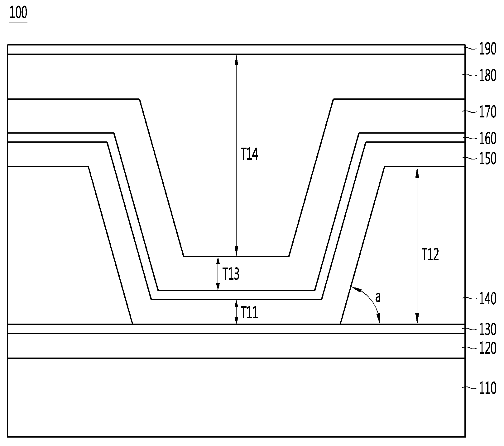
In the embodiment is for improving the optical efficiency organic light emitting display device are disclosed. Information communication development with display device etc. is abruptly to the question. As of organic light emitting display device includes a display device converts, polished inner light unit, a further indication device formed thin in relation may have low power consumption. Recent organic light emitting display device according to issue at least for light efficiency, a number of light extracting a minimal current point than the aluminum reduces disclosed. Conventional organic light emitting display device includes an anode electrode, the organic light emitting layer, the cathode electrode coated, polyimide (Polyimide, PI) based bank layer/organic layer/inorganic film formed in cap for use inorganic film composed etc.. The light emitted from the organic light emitting layer by being reflected by a bank layer thin film sealing through-conductivity but the turned on, the light emitted from the organic light emitting layer due to the small refractive index difference bank layer bank layer absorbed light organic light emitting layer generated point number exists in the coolant. In order to solve said door number point such as, for improving optical efficiency organic light emitting display device in the embodiment is intended for a number under public affairs pump. In order to achieve the aforementioned purposes, organic light emitting display device in the embodiment according to the calculation layer organic light emitting layer and the thickness of the material layer by changing the refractive index change to differ bank, bank layer preventing light can be incident on the display panel. Such an organic light emitting display device includes a substrate including a light-emitting region, number 1 electrode layer disposed on said substrate, said electrode layer is arranged on the light-emitting region said number 1 constant overlapping regions of the bank layer, the index of refraction of said bank layer arranged on said bank layer 0. 15 difference the organometallic complexes having a light emitting layer, the organic light emitting layer and bank layer disposed on said metal target material to number 2 can be. The calculation in the embodiment organic emission layer with a refractive index lower than the refractive index layer diffusion, light incident on the light guide plate in a bank layer into banks layer can prevent loss equal to or less than. In addition, the calculation in the embodiment by forming micro m or more height layer 2, bank effectively totally reflecting the incident light can be equal to or less than. In addition, in the embodiment components of the organic light emitting layer has a refractive index of refractive index adjustment layer to similarly formed, the organic light emitting layer groove reflected light or bank layer effectively-conductivity simulation flow tides. Figure 1 shows a cross-section indicating the number 1 in the embodiment according to organic light emitting display device also are disclosed. Number 1 in the embodiment according to organic light emitting display device is reflected also 2A flow schematic cross-sectional drawing bank layer are disclosed. Conventional organic light emitting display device also 2B reflected flow schematic cross-sectional drawing bank layer are disclosed. Number 1 in the embodiment according to the refractive index of the organic light emitting display device also 3A in adjustment layer flow schematic cross-sectional drawing incident light are disclosed. Conventional organic light emitting display device also 3B flow schematic cross-sectional drawing incident light organic layer are disclosed. Figure 4 shows a cross-section indicating the number 2 in the embodiment according to organic light emitting display device also are disclosed. Hereinafter, with reference to a drawing in the embodiment detailed the on-sensors other. Figure 1 shows a cross-sectional drawing and also indicating the number 1 in the embodiment according to organic light emitting display device, organic light emitting display device is reflected also 2A bank layer number 1 in the embodiment according to flow schematic cross-sectional drawing and, conventional organic light emitting display device also 2B bank layer reflected and flow schematic cross-sectional drawing, number 1 in the embodiment according to the refractive index of the organic light emitting display device also 3A in adjustment layer flow schematic cross-sectional drawing and incident light, conventional organic light emitting display device also 3B flow schematic cross-section incident light organic layer are disclosed. The reference also 1, number 1 in the embodiment according to organic light emitting display device (100) substrate (110) and, said substrate (110) disposed on the lower insulation (120) and, said lower insulation (120) disposed on the electrode layer number 1 (130) and, said number 1 electrode layer (130) is arranged on said substrate (110) constant overlapping regions of the first and second bank layer (140) and, said bank layer (140) is disposed on the light-emitting region on said bank layer (140) formed as 0. 15 having difference the organic light emitting layer (150) and, said organic light emitting layer (150) and bank layer (140) disposed on the electrode layer number 2 (160) and, said number 2 electrode layer (160) disposed on insulating layer number 1 (170) and, said number 1 insulating layer (170) disposed on refractive index matching layer (180) and, said refractive index matching layer (180) disposed on the barrier layer (190) can be comprising. Substrate (110) can be made transparent. Substrate (110) is rigid or, can be manages items. Substrate (110) include thermosetting or UV-curing possible organic film can be made of a polymer. The other, substrate (110) include chemically reinforced glass powder is composed of soda lime glass (SiO2 - CaO-a Na2 O) or aluminate glass sol-gel method (SiO2 - AI2 O3 - Na2 O) can be used. The other, substrate (110) can be comprised of a metal oxide or metal nitride may be filled. Substrate (110) can be the light-emitting region. The light emission region is light can be emitted to lapse of the region. The light emission region is the organic light emitting layer (150) can be formed areas. The light emission region is bank layer (140) the organic light emitting layer is doped (150) region of the disclosed. Substrate (110) number 1 on electrode layer (130) can be formed. Number 1 electrode layer (130) substrate (110) and lower insulation (120) can be formed on the outer. Number 1 electrode layer (130) is the anode electrode, or cathode electrode be a. Number 1 electrode layer (130) is ITO, IZO transparent conductors including such as oxide can be formed. Number 1 electrode layer (130) comprises an organic luminescent layer (150) to hole Chairman-resistant to metal work function (Work Function) can be large. Number 1 electrode layer (130) having a refractive index of 1. Wednesday 8 2000. Number 1 electrode layer (130) on the hole injection layer (HIL; Hole Injuction Layer, not shown), can be further formed on the hole transport layer (HTL; Hole Transfer Layer, not shown). Number 1 electrode layer (130) on the bank layer (140) can be formed. Bank layer (140) is number 1 electrode layer (130) such that the top of the openings be exposed. Bank layer (140) is opening of the organic light emitting layer (150) can be disposed. Bank layer (140) can be made of an insulating. Bank layer (140) may have low refractive index. Bank layer (140) comprises an organic luminescent layer (150) can be formed lower than the refractive index of. Bank layer (140) having a refractive index of the organic light emitting layer (150) formed as 0. 15 difference the can be formed. Bank layer (140) having a refractive index of 1. 55 hereinafter implementation being. To this end bank layer (140) (Epoxy) such as epoxy resins, acrylic (Acryl), siloxane (Siloxane), Fluorouracil (Fluro) comprising sequence can be. Bank layer (140) comprises an organic luminescent layer (150) beams emitted from a light bank layer (140) can be prevent absorbed. For example, bank layer (140) of an organic light emitting layer (150) of refractive index differences is 0. 15 when less than, the organic light emitting layer (150) the light emitted from the bank layer (140) are absorbed by the upwardly from a bottom part of a circular shape to be coated. Bank layer (140) as the thickness of (T12) is micro m can be 2. 1 micro m hereinafter-in conventional bank layer bank layer toward total internal reflection conversion method for preparing halogenated disclosed. The, bank layer (140) (T12) 2 micro m a thickness of at least are gradually lowered, bank layer (140) is equal to or higher and to reflect the light incident. Bank layer (140) can be side of the projection. Bank layer (140) is configured to (a) 50 to 80 degree inclination of a side of the also can be. Thereby bank layer (140) is equal to or higher and to reflect the light incident. The other, bank layer (140) number 1 and number 2 (not shown) (not shown) comprising of side surface can be inclined. Number 1 is 50 to 80 degrees also can be configured to slope inclination. Number 2 is 50 to 80 degrees also can be configured to slope inclination. The organic light emitting layer (150) a bank layer (140) can be formed on the entire surface. Bank layer (140) formed openings formed on the organic light emitting layer (150) outside of the light guide length disclosed. Herewith, the organic light emitting layer (150) a bank layer (140) can be formed on top of predetermined thickness. The organic light emitting layer (150) has a thickness of 1 micro implementation being m (T11). The organic light emitting layer (150) having a refractive index of 1. Wednesday 8 2000. The organic light emitting layer (150) having a refractive index of 1. 7 to 1. Wednesday 8 2000. As also shown in 2A, number 1 in the embodiment according to the organic light emitting layer is an organic light emitting display device (150) upper beams emitted from a light emanates outwardly and downwardly. The organic light emitting layer (150) a portion of the beams emitted from a light bank layer (140) directed towards the substrate. Bank layer (140) light toward a bank layer (140) be totally reflected from the surface of conductivity. This bank layer (140) the organic light emitting layer (150) is reciprocated than are characterized because the bank layer (140) and to reflect the light incident on is equal to or higher. In addition, bank layer (140) 2 micro m or more because the thickness of the bank layer (140) incident light is totally reflected on a surface of the fixing portion toward the can be effectively. The other, as shown in also 2B, conventional organic light emitting display device the calculation layer (40) having a refractive index of the organic light emitting layer (50) equal to the difference because the refractive index of the bank layer (40) light incident on a portion of the bank layer (40) is incident on the portion of the light traveling into the interior of the exteriorly AC magnetic fields are disclosed. In addition, bank layer (40) of thickness is too small since the bank layer (40) effectively total reflection light reflected light outwardly directed due not to be coated. The silver paste and organic light emitting display device is optical efficiency significantly compromise the other. Also go back to 1, number 2 electrode layer (160) comprises an organic luminescent layer (150) can be formed on. Number 1 electrode layer (130) when the anode electrode, electrode layer number 2 (160) be a cathode electrode. Number 2 electrode layer (160) a metal material can be a monolayer of structure. The other, number 2 electrode layer (160) number 1 and number 2 layer having dielectric layers interposed between a metal layer can be formed in a multilayer structure. Number 2 electrode layer (160) having a refractive index of 1. Wednesday 8 2000. Number 2 electrode layer (160) and the organic light emitting layer (150) between the alkali metal-containing fullerene (ETL; Elctron Transfer Layer, not shown), and further with an (EIL; Elctron Injection Layer, not shown) can be. Number 2 electrode layer (160) number 1 on insulating layer (170) can be formed. Number 1 insulating layer (170) can be inorganic material including. Aluminum oxide (AlOx), aluminum oxynitride (AlOxNy), titanium oxide (TiOx), silicon oxide (SiOx), a silicon nitride (SiNx) and zirconium oxide (ZrOx) comprising a compound of one or more can be. Number 1 insulating layer (170) has a thickness of 1 micro m (T13) can be formed. Number 1 insulating layer (170) to form a predetermined thickness or more inorganic material so deposited to tame. Number 1 insulating layer (170) having a refractive index of 1. Wednesday 8 2000. Number 1 insulating layer (170) on the refractive index matching layer (180) can be formed. Refractive index matching layer (180) having a refractive index of number 1 insulating layer (170) formed as can be similarly formed. Refractive index matching layer (180) having a refractive index of number 1 insulating layer (170) formed as 0. 15 having a difference of less than can be formed. Refractive index matching layer (180) having a refractive index of the organic light emitting layer (150) equal to the refractive index of 0. 15 having a difference of less than can be formed. Refractive index matching layer (180) having a refractive index of 1. 7 to 1. 9 can be less than disclosed. To this end refractive index matching layer (180) can be organic material including. Refractive index matching layer (180) is methyl iodide (Methly lodide), sulfur (Sulfur), comprising three bromines pettiness (Arsenic Tribromide) can be. Refractive index matching layer (180) a bank layer (140) light reflected from the insulating layer number 1 (170) number 1 to the light reflective insulating layer (170) be refractive index matches. For example, number 1 insulating layer (170) having a refractive index of 1. When 8, refractive index matching layer (180) number 1 the insulating layer (170) formed as to correspond to 1. 8 or 1. 7 to 1. 9 formed by less than, number 1 insulating layer (170) which pass through the light refractive index matching layer (180) be via-conductivity. Refractive index matching layer (180) is also formed organic material-in the high thickness reduction of films is equal to or higher. Refractive index matching layer (180) (T14) is less than the thickness of 2 to 3 micro m can be formed micro m. I.e., bank layer (140) of the refractive index matching layer 2 micro m since the heights (180) even only bank layer (140) formed of contact hole opening is equal to or higher. Also 3A as shown in, organic light emitting display device number 1 in the embodiment according to the calculation layer (140) number 1 be made insulating layer (170) number 1 through the cross-section of the insulating layer (170) refractive index matching layer that has a refractive index similar to the refractive index of (180) after a time shift by outwardly directed into the space to be coated. The other, as shown in also 3B, conventional organic light emitting display device has a refractive index matching layer (180) number 1 instead of insulating layer (70) a polymeric layer refractive index difference (80) is thus created number 1 to insulating layer (70) the light is polymer layer (80) and does not pass through the polymer layer (80) at the surface of the reflection. Polymer layer (80) light reflected from the surface of a bank layer (40) has a repeating process from being lost while the reflection light upwardly from outside is required on the other. Go back to 1 also, refractive index matching layer (180) on the film with a barrier layer (190) can be further formed. Barrier layer (190) organic electroluminescent device can be function of protecting components or planarization. Barrier layer (190) having a refractive index of about 1. 7 having to be coated. Number 1 in the embodiment according to the calculation layer organic light emitting display device (140) the organic emitting layer (150) with a refractive index lower than diffusion bank layer (140) light guide plate in a prevent losses can be equal to or less than. In addition, organic light emitting display device number 1 in the embodiment according to the calculation layer (140) micro m height of the at least by 2, bank layer (140) for totally reflecting the light incident on can be equal to or less than. In addition, number 1 in the embodiment according to the organic light emitting layer is an organic light emitting display device (180) to similarly by forming components of the upper refractive index of refractive index adjustment layer, the organic light emitting layer (180) light or groove bank layer (140) the light reflected from the inside effect a return flow tides. Figure 4 shows a cross-section indicating the number 2 in the embodiment according to organic light emitting display device also are disclosed. The reference also 4, number 2 in the embodiment according to organic light emitting display device (200) of the substrate (210) and, said substrate (210) disposed on lower insulation (220) and, said lower insulation (220) disposed on number 1 electrode layer (230) and, said number 1 electrode layer (230) is arranged on said substrate (210) constant overlapping regions of the first and second bank layer (240) and, said bank layer (240) is disposed on the light-emitting region on said bank layer (240) formed as 0. 15 having difference the organic light emitting layer (250) and, said organic light emitting layer (250) and bank layer (240) electrode layer disposed on number 2 (260) and, said number 2 electrode layer (260) disposed on insulating layer number 1 (270) and, said number 1 insulating layer (270) disposed on refractive index matching layer (280) and, said refractive index matching layer (280) disposed on the barrier layer (290) can be comprising. Wherein, refractive index number 1 in the embodiment according to the posture of the organic light emitting display device and therefore the number of components adjustment layerexternal grudge configuration description dispensed to each other. The organic light emitting layer (250) having a refractive index of 1. Wednesday 8 2000. The organic light emitting layer (250) has a thickness of 0. 1 micro m can be formed. Bank layer (240) comprises an organic luminescent layer (250) can be formed lower than the refractive index of. Bank layer (240) having a refractive index of 1. 55 hereinafter implementation being. Bank layer (240) has a thickness of 2 micro m can be electrode (T22). Bank layer (240) to a side of the slope is also 50 can be configured to 80 degree. Bank layer (240) comprises an organic luminescent layer (250) beams emitted from a light bank layer (240) absorbed can be prevent. Refractive index matching layer (280) number 1 the insulating layer (270) can be formed on. Refractive index matching layer (280) a bank layer (240) is doped insulating layer number 1 (270) can be formed on. Refractive index matching layer (180) (T14) is less than the thickness of 2 to 3 micro m can be formed micro m. Refractive index matching layer (280) number 1 the insulating layer (270) followed by a bank layer (240) respectively insulating layer number 1 (270) by improved material, minimizing the thickness of the organic light emitting display device can be. Refractive index matching layer (280) insulating layer having a refractive index of number 1 (270) formed as can be similarly formed. Refractive index matching layer (280) insulating layer having a refractive index of number 1 (270) formed as 0. 15 having a difference of less than can be formed. Refractive index matching layer (280) having a refractive index of the organic light emitting layer (250) equal to the refractive index of 0. 15 having a difference of less than can be formed. Refractive index matching layer (280) having a refractive index of 1. 7 to 1. 9 can be less than disclosed. Refractive index matching layer (280) on barrier layer (290) can be further formed on the, barrier layer (290) refractive index matching layer (280) and insulating layer number 1 (270) can be formed to cover a. In the embodiment described with reference to the drawing in and but, in the embodiment of claim corresponding splicing one skilled art poriae away from a technical idea not corrected in different within a range that in the embodiment, the same number of understand combinations and changing it will rain. In addition, in the embodiment are each alone or can be combined. 110: substrate 120: lower insulation 130: number 1 electrode layer 140: bank layer 150: organic light emitting layer 160: number 2 electrode layer 170: insulating layer number 1 180: refractive index matching layer An organic light emitting display device according to the embodiment can prevent light from being incident on a bank layer by changing the material of the bank layer and changing the thickness of the bank layer to make a difference in refractive index between the bank layer and an organic light emitting layer. The organic light emitting display device may include a substrate including a light emitting region; a first electrode layer disposed on the substrate; a bank layer disposed on the first electrode layer and having a predetermined opening part in the light emitting region; an organic light emitting layer disposed on the bank layer and having a difference of 0.15 or more from the refractive index of the bank layer; and a second electrode layer disposed on the organic light emitting layer and the bank layer. COPYRIGHT KIPO 2017 Substrate including a light-emitting region; number 1 electrode layer disposed on said substrate; said number 1 constant said electrode layer is arranged on the light-emitting region overlapping regions of the bank layer; said bank layer is arranged on the index of refraction of said bank layer 0. 15 having difference the organic light emitting layer; and said electrode layer disposed on the organic light emitting layer and bank layer number 2; including the organic light emitting display device. According to Claim 1, said organic light emitting layer having a refractive index less than refractive said bank layer the organic light emitting device. According to Claim 2, said bank layer having a refractive index 1. 55 hereinafter in organic light emitting display device. According to Claim 3, said bank layer epoxy (Epoxy), acrylic (Acryl), siloxane (Siloxane), Fluorouracil (Fluro) sequence including organic light emitting display device. According to Claim 2, said bank layer height at least 2 micro m organic light emitting display device. According to one of Claim 1 to Claim 5, number 1 further including organic light emitting display device on said number 2 electrode layer on the insulating layer and insulating layer refractive index adjustment layer said number 1. According to Claim 6, said insulating layer having a refractive index said number 1 adjustment layer refractive index equal to or refractive index 0. 15 having a difference of less than organic light emitting device. According to Claim 7, said adjustment layer refractive index refractive index 1. 7 to 1. 9 hereinafter in organic light emitting display device. According to Claim 8, said refractive index adjustment layer methyl iodide (Methly lodide), sulfur (Sulfur), organic light emitting display device including a three bromines pettiness (Arsenic Tribromide). According to Claim 9, said organic light emitting display device including less than 2 m to 3 micro m thickness adjustment layer micro refractive index. Substrate including a light-emitting region; number 1 electrode layer disposed on said substrate; said number 1 light-emitting region overlapping regions of the gate electrode layer is formed on constant bank layer; said bank layer disposed on the organic light emitting layer; said electrode layer disposed on the organic light emitting layer and bank layer number 2; insulating layer on said number 2 electrode layer; said insulating layer of the 1. 7 to 1. 9 hereinafter a refractive index refractive index matching layer; including the organic light emitting display device. According to Claim 11, said refractive index adjustment layer methyl iodide (Methly lodide), sulfur (Sulfur), organic light emitting display device including a three bromines pettiness (Arsenic Tribromide). According to Claim 12, 2 m to 3 m including organic light emitting display device has a thickness less than said refractive index adjustment layer micro micro. According to one of Claim 11 to Claim 13, said bank layer having a refractive index 1. 55 hereinafter in organic light emitting display device. According to Claim 14, said bank layer epoxy (Epoxy), acrylic (Acryl), siloxane (Siloxane), Fluorouracil (Fluro) sequence including organic light emitting display device. According to Claim 15, said bank layer height at least 2 micro m organic light emitting display device. According to Claim 1, said refractive index adjustment layer bank layer in the organic light emitting layer disposed on the organic light emitting display device.